downloadGroupGroupnoun_press release_995423_000000 copyGroupnoun_Feed_96767_000000Group 19noun_pictures_1817522_000000Member company iconResource item iconStore item iconGroup 19Group 19noun_Photo_2085192_000000 Copynoun_presentation_2096081_000000Group 19Group Copy 7noun_webinar_692730_000000Path
Skip to main content
Default Banner Image

Artificial Intelligence

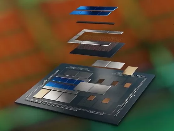
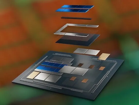
As monolithic scaling slows down, the semiconductor industry is increasingly relying on advanced packaging technologies to extend Moore’s law through heterogeneous integration. Higher on-package bandwidth, improved yield resiliency and the need to integrate diverse IP from multiple foundries are driving demand for advanced packaging technologies that address these issues but introduce challenges of their own such as efficient power delivery to all the different domains in a heterogeneous system. SEMI spoke with Kaladhar Radhakrishnan, Intel Fellow at Intel, about heterogeneous system integration trends and new developments in the semiconductor industry. Radhakrishnan shared his views ahead of his keynote at the SEMI Connecting Heterogeneous Systems Summit, 1-3 September 2021, an online event. Join the summit to meet experts from Intel and other key industry influencers. Registration is open. SEMI: What is driving the adoption of electronics and semiconductor devices nowadays and why is the development of new and innovative technologies important? Radhakrishnan: We are living in an increasingly data-driven world where devices have become an integral part of our lives. A recent study estimated that in the United States alone, 13.6 connected devices per capita consume an average of 300 gigabytes worth of data every month. In the workplace, COVID-19 has driven fundamental business changes that has sped up the adoption of digital technologies such as virtual conferencing, remote work, and e-commerce. Organizations are realizing that a high-quality video conference can be an adequate substitute for many in-person meetings. As a result, businesses are accelerating the digital transformation in order to adapt and thrive in this new environment. Five decades of sustained exponential growth in semiconductor performance has conditioned the average digital consumer to expect more from their devices. However, there are some headwinds ahead as traditional scaling slows down and power density rises. Because consumers and businesses are now generating data at a faster rate than they can consume it, technologists need to scale compute, storage, and bandwidth even faster to keep pace. Without investments in research and development of new and innovative technologies to address these challenges, the full potential of this data will go unrealized. SEMI: What forces are heightening the importance of heterogeneous system integration? What are the implications for increased on-package bandwidth, improved yield resiliency and the need to integrate diverse IP from multiple foundries? Radhakrishnan: The semiconductor industry increased transistor density and scaled performance through classical Dennard scaling until the turn of the century. By then, the gate oxide thickness had scaled down to atomic dimensions and the exponential increase in sub-threshold leakage signaled the end of scaling through traditional methods. Since that time, the chip industry has been relying on innovations in transistor materials and structures such as high-k metal gate, strained silicon, and FinFETs to keep pace with Moore’s law. However, this alone will not be sufficient to continue scaling and the industry needs to explore other vectors to augment improvements in transistor technology. Heterogeneous integration through advanced packaging is one key technology that can help drive these gains. Technologies like Foveros can enable device density scaling by creating a 3D stack of multiple die using high-density interconnects. Heterogeneous integration enables chipmakers to move from a monolithic system designed on a single large chip to a heterogeneous system comprised of a number of smaller chiplets. The main benefit of using smaller chiplets is that they improve yield and enable application based customization of the foundry processes. However, if the disaggregation to smaller chiplets is not accompanied by an increase in on-package bandwidth, the power and performance penalties associated with chiplet-to-chiplet communication will hobble system performance. This is why advanced packaging technologies that improve die-to-die communication are key enablers for heterogeneous integration. SEMI: What are some of the key technology challenges in developing heterogeneous systems? Radhakrishnan: The obvious challenge that most people focus on is the need for improved on-package bandwidth. However, as we rely on 3D stacking to continue device scaling at the package level, it is important to comprehend power delivery and thermal challenges as well. Power to the top die has to be delivered through TSVs on the bottom die, which not only adds resistance but also reduces the useful area available on the bottom die. This problem is further exacerbated when we stack more than two die. Excessive noise on the power delivery network can cause timing issues that limit the maximum operating frequency of the transistor. Similarly, when we stack multiple die, we must take into account associated thermal challenges. For example, each interface of the multi-die stack adds thermal resistance, which makes it harder to cool the chips at the bottom. SEMI: What are some of the key global market trends that driving demand for heterogeneous and system-level integration? Radhakrishnan: The number of artificial intelligence (AI) and machine learning applications have grown dramatically due to their ability to solve highly complex problems across a wide range of segments. AI and machine learning models require more memory bandwidth and compute capabilities that are difficult to achieve without some form of heterogeneous integration. Another market trend driving demand for heterogeneous integration is the increasing reliance on custom hardware accelerators. To combat the slowdown in frequency scaling and single-core performance, we have moved to multi-core architectures by tackling the inherent parallelism in our workloads. However, Amdahl’s law tells us that such an approach will hit a bottleneck when we reach the limits of the serial portion of the workload. As these constraints slow the performance of general-purpose processors, the reliance on custom hardware accelerators to boost performance for specific workloads is growing. Heterogeneous integration at the system level with a combination of CPUs, GPUs, FPGAs and other accelerators can optimize system power and performance. SEMI: What solutions is Intel developing to address these market needs? Radhakrishnan: Intel is actively involved in the development of the industry ecosystem for heterogeneous integration. We have developed a number of innovative advanced packaging solutions such as the EMIB and Foveros that are used in products today. Intel is also developing the next generation of advanced packaging technologies, Foveros Omni and Foveros Direct, which will dramatically scale the IO density by using direct Cu-Cu bonding technology. Foveros Omni is a crucial building block technology to enable high-voltage power conversion on the package for efficient power delivery. Intel is uniquely positioned to predict the design needs for future systems and deploy its resources to develop the technology building blocks needed to continue performance scaling. Our IDM 2.0 strategy enables us to leverage our leadership in packaging technologies to design the best products and use the best IP to deliver leading products across a broad range of categories. SEMI: What do you expect from your participation at SEMI Connecting Heterogeneous Systems Summit? Radhakrishnan: I’m hoping to shed some light on some of the new technologies we have been developing at Intel to enable heterogeneous system integration. I also want to bring awareness to the power-related challenges we are facing with heterogeneous systems. I also look forward to listening to what other industry leaders have to say on the topic. Kaladhar Radhakrishnan is an Intel Fellow and a Power Delivery Architect with the Technology Development group at Intel. He plays a significant role in shaping and driving power delivery technologies for Intel microprocessors. His areas of expertise include integrated voltage regulators, advanced packaging and passives technologies. Kaladhar is a two-time recipient of the Intel Achievement Award, the highest Intel honor an individual or small team can receive. He has authored four book chapters, over 40 technical papers in peer-reviewed journals, and has been awarded 35 U.S. patents. He has also served as an adjunct professor at Arizona State University. Kaladhar joined Intel in 2000 soon after receiving his Ph.D. in Electrical Engineering from the University of Illinois at Urbana-Champaign. Serena Brischetto is senior manager of marketing and communications at SEMI Europe.
Read More
Spend any time with Ansys’ John Lee, Rich Goldman or Marc Swinnen and you’ll hear plenty of optimism about the semiconductor industry even though they tick off a long list of looming design challenges. The need for reliable and effective electronic systems, they emphasize, is great and runs through high tech, aerospace and defense, automotive, IoT and 5G with communications being a common denominator. The three are especially bullish these days on changing market dynamics brought on by systems companies building company-specific bespoke, or custom, silicon. These systems companies are building chips with a different perspective and a fresh look at silicon design, a move away from the more traditional segment-specific silicon due to much more complexity. Ansys, a member of the ESD Alliance, a SEMI Technology Community, is a 4,100-employee company with a comprehensive portfolio of multiphysics engineering simulation software for product design, testing and operation products and services. John, Rich, Marc and I focused on Ansys’ semiconductor and electronics segment for our conversation. Smith: When did you notice the move by systems companies to build their own chips? What drives this trend? Lee: The inflection point was about three years ago when hyperscale data center and system companies recognized they needed an enterprise system design platform. They are designing bespoke silicon, driven to do this for cost efficiencies and to avoid relying on outside suppliers. They also want differentiation based on their specific platform needs so they can optimize compute power to their specific needs. Smith: What is driving the trend for multiphysics experience to ensure effective and reliable electronic systems? Lee: The increasing need for multiphysics analysis is acute. The physics of 3D IC, for example, brings in mechanical engineering with the convergence of mechanical and electrical as 3D emerges at the intersection of IC and System. As a result, physics becomes a necessity to analyze the stability of the chip in the package. Goldman: As well, the move to stacked chips, 3D IC and wafer-on-wafer requires thermal, electromagnetic and mechanical analysis in addition to the traditional analysis for function, performance and power. They all need to be analyzed together, not serially. It becomes multiphysics, not multiple physics. Smith: Two distinctly different disciplines – multiple physics and multiphysics – are needed for semiconductor design. How are they different? Why the need now? Swinnen: Multiple physics refers to the sheer breadth of physics that is now needed to analyze from the IC up to the largest system whereas multiphysics refers to the capability to analyze several physical effects concurrently, accounting for their impact on the design and interactions between various physics. Multiphysics are necessary to analyze the full context of the system environment – from nanometers to kilometers – for multi-chip packaging, chip-to-package-to-silicon and systems with multi-domain guidance. Goldman: A self-driving car, as an illustration, includes AI systems-on-chip, solid-state sensors, infotainment systems and radar/lidar detectors that must all work in the rain, the heat and the bitter cold. Smith: Why are design groups being reorganized to include expertise in mechanical and electromagnetic issues? Swinnen: Complexity has exploded, driven by a long list of technical requirements and, perhaps, mischaracterization. Goldman: Just consider the system on chip, mischaracterized by the semiconductor industry. The chip is never a system by itself. Rather, it is a complex component in a larger system and must be analyzed in that context. 3D IC is where this comes together and forces a recognition of physics outside the traditional scope of SoC design. 3D IC chips are much closer together on the board and it takes multiphysics embedded into the workflow of semiconductor design, packaging, system design and 3D IC to ensure they work reliably and efficiently. Smith: What is the solution? Goldman: It’s clear a specialized digital thread is necessary to move disparate groups with expertise in systems, physics and silicon together. Today, these groups or disciplines might not exist in the same company, whether it be a foundry, fabless or outsourced semiconductor assembly and test (OSAT) company. Lee: In order to unify the entire system design environment, a cloud-based, open and extensible heterogenous enterprise compute platform is required. It is similar to the SaaS-based business model and known as Simulation-as-a-Service (also SaaS). While vertical integration of design groups is already taking place at leading system design houses, there have also been advances in electronic design tools. These are starting to offer more comprehensive multiphysics capabilities including thermal, fluid dynamics (CFD), mechanical stress and reliability analysis in a single analysis cockpit. Today’s system designers face two platform challenges: First, they need an environment that is open enough to accept analysis results from multiple sources so that they can be overlapped and cross-analyzed. Second, the design platform must have the capacity to handle the enormous amounts of data generated by the latest 3-nanometer chips and 3D IC systems, and this implies an intimate coupling to elastic cloud computing. The days of an engineer writing Perl scripts and handing it off to someone else are gone. We believe that the industry is responding to this challenge with a new generation of design platforms that a cloud-native, open and extensible to allow heterogenous enterprise design. We are definitely at an inflection point in electronic design today, but the electronic industry has faced these before an we are confident it will master these challenges as well. About Rich Goldman Rich Goldman is director of marketing for the Electronics and Semiconductor Business Unit of Ansys. He holds a Bachelor of Science degree from Syracuse University and an MBA and Master of Science degree in Engineering Management. Moscow Institute of Electronic Technology (MIET)’s first honorary professor, he is also the recipient of honorary PhD degrees from Russian-Armenian (Slavnoic) University and State Engineering University of Armenia for contributions to the advancement of Armenia’s high-tech education and economic ecosystem. Rich served on EDAC’s board of directors. About John Lee John Lee is general manager and vice president of the Ansys Electronics and Semiconductor Business Unit. Lee co-founded and served as CEO of Gear Design Solutions (now Ansys), developer of the first purpose-built big data platform for integrated circuit design. He cofounded two other startups (Mojave Design and Performance Signal Integrity), which successfully exited into companies now part of Synopsys. He holds undergraduate and graduate degrees from Carnegie Mellon University. About Marc Swinnen Marc Swinnen is director of product marketing for the Electronics and Semiconductor Division of Ansys. He holds Master degrees in Electronic Engineering and Industrial Management from KU Leuven, Belgium, as well as an MBA from San Jose State University. About Bob Smith Robert (Bob) Smith is executive director of the ESD Alliance, a SEMI Technology Community. He is responsible for the management and operations of the ESD Alliance, an international association of companies providing goods and services throughout the semiconductor design ecosystem.
Read More
The state of manufacturing is changing rapidly. Regardless of sector or location, manufacturing decision-makers across the world are signaling a desire for better supply chain resiliency, manufacturing flexibility, increased speed of innovation and stronger environmental sustainability. Singapore’s manufacturing sector, a significant contributor to its gross domestic product, is always evolving and today is shifting away from its traditional focus on producing highly customized products using flexible manufacturing processes, but at significantly lower efficiencies. Today, with Industry 4.0, we can design manufacturing systems that optimize both efficiency and flexibility. And this is possible because of the convergence of technologies such as artificial intelligence (AI), data analytics, robotics and the Industrial Internet of Things (IIoT). This blend of technologies helps reduce the cost of technological solution ownership – a derivative of Right’s Law – as a function of cumulative production. In HP Singapore, driving innovation in our product and processes is part of our DNA, and over time our products have grown in complexity and breadth. We have embraced Fourth Industrial Revolution (4IR) technologies in our advanced manufacturing lines. We started our Industry 4.0 journey in 2016 with Vision and Mission 2020 to modernize our production facilities to smart factories that strengthen our competitive edge. Our focus was on upskilling our employees with future skill sets, build new technological capabilities and partner with higher education institutes. To drive these transformations, we have formulated five pillars: Additive Manufacturing Data Analytics Cyber-Physical Integration Digitalization Workforce Transformation These five pillars have enabled us to move from labor-intensive and reactive processes to processes that are highly digitized, automated, and AI-driven, enabling us not only to increase quality and productivity but also to reskill our people in anticipation of jobs they will need in the future. Technicians have been upskilled and promoted to techno-operators which has, in turn, freed up technical specialists to explore other roles. Engineers have retrained as data scientists, or have moved to new product development, for instance. In 2017, HP’s Ink Supplies Operations (ISO) set up Smart Manufacturing Applications and Research Centre (SMARC) to adopt 4IR technologies and implement these innovations in production lines. Today, SMARC is the home ground for HP engineers to experience, trial and prototype solutions, bringing innovative and sometimes unexpected solutions to manufacturing. It is also a showcase for industry partners, government agencies and schools. Here is how each pillar of the SMARC contributed to transformation to augment the manufacturing workforce: Cyber-Physical Integration – Move Role of robotics/automation – By standardizing automation standards for robotics, we have deployed collaborative robots (Cobots) and autonomous intelligent vehicles (AIVs) to perform manual and routine tasks to drive productivity, while reducing errors from operator fatigue and protecting our operators’ physical well-being. Digitalization – Sense Role of IIoT – Devices are a treasure trove of data that can provide clarity on how the entire manufacturing line is performing in real time. Building a platform that connects devices and collects data while allowing factory floor managers to dynamically visualize on an Integrated Command Centre (ICC) and manage factory performance is central to HP’s digital transformation journey. And IIoT is not restricted to just devices that are already wired for data sharing. HP has also connected off-the-shelf analogue devices using a standardized data transportation protocol, allowing HP to collect essential data across all types of devices and eliminating manual data entry. Additive Manufacturing – Build By embracing additive manufacturing (use of HP MultiJet Fusion 3D printers), HP introduced more flexibility in operations through on-site rapid prototyping, light production, and replacement of parts needed on our manufacturing floors, shortening production timelines. We 3D printed pallets, which are cheaper and faster to produce, and replaced original pallets for transportation on conveyor belts, improving the efficiency and productivity of our operators. Director Jamie Neo with HP’s MultiJet Additive Manufacturing Printer. (Photo Credit: HP) The HP Multi Jet Fusion 3D printing technology has helped HP to replace traditional manufacturing methods and streamline processes in our supply chain. For example, HP is 3D printing the Drill Extraction Shoe, a tool that is essential to the removal of waste products from laser-drilling in HP’s printhead manufacturing line. Through 3D printing, HP has consolidated the production of the tool from nine parts to one 3D printed model, thereby optimizing the design of the tool and reducing its production time from three to five days to 24 hours. Data Analytics – Think By deploying advanced analytics and machine learning models, HP has enabled real-time detection, diagnostics, and prediction of product quality across our manufacturing lines. Predictive models are replacing traditional “destructive testing,” reducing waste and allowing HP to meet unique product specifications more accurately. Machine learning is diagnosing and recommending the right set up for tools and manufacturing lines, when necessary, to reduce downtime and increase precision. Workforce Transformation – Grow The pivot to becoming an advanced manufacturing leader not only requires HP to invest in 4IR technologies but also skill sets to operate 4IR technologies. We embarked on a Workforce Transformation program to help our employees stay competitive in a fast-changing world. Today 35% of HP technical workforce have had the opportunity to take on new roles even as needs evolve, thanks to internal and external training and reskilling. Beyond technology and training, the glue that binds these together and makes it successful is our culture at HP. We are ambition-led, which means that we do not see the world as it is, but what we can be. And we do so by collaboration. Plans for the Future After accomplishing our Mission 2020, in late 2020 we launched Mission 2025 to extend our end-to-end smart factory capabilities through advanced connectivity, intelligence and automation to optimize and drive sustainable manufacturing flexibility and efficiency. Pyramid of HP’s smart manufacturing focus Advanced technologies such as additive manufacturing, IIoT, automation and robotics, data analytics, machine learning and AI are central to the connectivity and the end-to-end intelligence of our smart factories, enhancing production efficiency and flexibility while improving the quality of our products. For example, the deployment of IIoT sensors in our wafer plant has helped to reduce downtime in replacing CO2 gas cylinders. What’s more, AI enables us to more accurately monitor the dispensing of structural adhesive to eliminate lost yield. We believe that by enhancing manufacturing efficiency and flexibility, we were able to shorten resolution time, reduce our carbon footprint, and improve the resiliency of our manufacturing and supply chain systems. HP smart factory model In April 2021, two lines in HP Singapore joined the World Economic Forum’s Global Lighthouse Network after being recognized for pivoting from a labor-intensive factory into a digitized, automated one with the help of AI. In doing so, we managed to improve manufacturing costs by 20% and productivity by 70%. Under Mission 2020, we saw the following successes: Improved manufacturing costs by 20% Improved productivity by 70% Brought most HP employees onboard to our smart manufacturing journey Equipped HP employees with skill sets in areas such as additive manufacturing, data analytics, AI, robotics and Internet of Things Established a Model Factory playbook With Mission 2025, we will: Continue to train employees in future skillsets by partnering with institutes of higher learning Scale our Model Factory playbook across more manufacturing lines to reduce costs and improve productivity Enhance our knowledge in additive manufacturing by building an ecosystem as a service platform to help manufacturing companies Enable a sustainable manufacturing system to reduce our carbon footprint and help enable a circular economy We believe in innovating with purpose by focusing on solving real-world problems and creating technology in the service of humanity. That is why we built the SMARC to create the solutions for our lines and showcase these solutions to encourage industry participation. We are driven by values and ambition, which means that it is not just what we do, but also how we execute it. We make sure our values inform everything we do – for instance, helping us make a greater impact to environmental sustainability, people, and our community. We believe this is a crucial step in coalescing industry support, which is necessary to move the needle on advanced manufacturing. Robert Ronald is Master Program Manager, Cost Structure, Model Smart Factory and Sustainability, at HP.
Read More
In the span of a few short months earlier this year, Mentor Graphics became Siemens EDA and introduced a suite of integrated hardware-assisted verification tools, the first product launch under the new Siemens EDA brand. Jean-Marie Brunet, senior director of marketing, product management and product engineering at Siemens EDA, orchestrated the launch and connected with me for a discussion about the chip design verification space. As he pointed out, verification and validation of systems is a fast-growing and important market segment to the electronic system design ecosystem. Smith: What trends do you see in chip design? What is driving these trends? Brunet: Chip verification costs continue to grow faster than design costs because of factors such as increasing design complexity, rising computing power, surging I/O traffic activity, increasing energy consumption and the widespread use of peripherals. These dynamics are being driven by new data center networking, communications/5G, autonomous driving, artificial intelligence (AI) and machine learning (ML), and storage applications. These trends also indicate the need for more powerful verification tools and expanded verification objectives that include power and performance analysis. Hardware-assisted verification tools are perfect for meeting these demands. Smith: Chip design verification consumes the most time in a project cycle. Why is this so? Brunet: The verification of designs reaching multi-billion gates and supported by voluminous software stacks is fraught with challenges. To exhaustively check every possible state in a billion-gate design with simulation alone would require up to trillions of verification cycles. That’s why hardware-assisted verification is one of the fastest-growing technologies in EDA. Given the complexity of today’s SoC design, it’s no surprise that verification is the largest undertaking in the entire project design cycle, consuming more than 50% of it. It also has the greatest impact on quality, cost and schedule because it prevents designs from failing at first silicon. While a respin of a large design taped out at a node below 10 nanometers could cost more than $10 million, delaying delivery of a new product for a few months in a highly competitive market may cost hundreds of millions of dollars. Smith: What other challenges do engineers face trying to verify a chip design will work as intended? Brunet: Verifying an SoC design is a massive undertaking and, in parallel, verification teams are trying to streamline and optimize verification cycles. SoC design groups are tasked with completing full system-level verification prior to creating production masks by thoroughly vetting all hardware blocks, interactions between those blocks, and the software developed for the end application before the chip is built. To alleviate this enormous pressure, they are starting to adopt a shift-left methodology for early functional verification as soon as individual blocks of a SoC design become available. It helps jump-start embedded software validation before full system validation is completed to save time and allow engineers to work in parallel, not serially. While it is an effective approach, it creates the need for a complete and integrated suite of hardware-assisted verification tools to verify and validate a design’s hardware and software components. Smith: How do you define hardware-assisted verification and how does it help solve these challenges? Brunet: A typical definition of hardware-assisted verification is special purpose hardware to accelerate verification. In other words, hardware emulation and FPGA prototyping. Hardware-assisted verification is a mandatory investment as single-die or multi-die chips get larger with more complexity and more interfaces, making hardware and software code integration critical early in the design cycle. Because software performance defines a chip’s success, the need to perform software workload-based analysis is acute, not just analysis of chip functionality, but also accurate performance and power consumption in the context of real-world applications. Hardware-assisted verification is the only option when hardware and software meet. By combining emulation, desktop FPGA prototyping boards and enterprise FPGA prototyping platforms to work on the same SoC design, a verification group can assemble a complete hardware-assisted verification system for thorough and exhaustive verification and validation. Smith: Where are the big opportunities for hardware-assisted verification? Brunet: New end-user applications are coming from computing and storage, AI/ML, 5G, networking and automotive. Recently released market data from the ESD Alliance shows that in 2020, hardware-assisted verification revenues exceeded $700 million. It is reasonable to assume that revenues of $1 billion will be within reach in the next few years given the amount of chip design activity at advanced nodes below 10nm. Smith: With the design/verification and manufacturing phases of the semiconductor supply chain more closely aligning, what role does hardware-assisted verification play? Brunet: Semiconductor manufacturing and the supply chain that supports it benefits greatly from the continued innovation in verification and validation tools and methodologies. With this innovation, designs are delivered to the manufacturing flow with a much greater chance of passing first silicon with success. This reduces friction in the semiconductor supply chain since IP and chips are available when anticipated. Hardware-assisted verification is a quick-moving, highly leveraged resource that helps a design and verification team to ensure chips are manufacturable and meet the functionality, power and performance requirements for the end-product application. Jean-Marie Brunet is the senior director of product management and engineering for the Scalable Verification Solutions Division at Siemens EDA. He has served for over 20 years in application engineering, marketing, and management roles in the EDA industry, and has held IC design and design management positions at STMicroelectronics, Cadence, and Micron, among other companies. Jean-Marie holds a Master's degree in Electrical Engineering from I.S.E.N Electronic Engineering School in Lille, France. Jean-Marie Brunet can be reached at [email protected]. About Bob Smith Robert (Bob) Smith is executive director of the ESD Alliance, a SEMI Technology Community. He is responsible for the management and operations of the ESD Alliance, an international association of companies providing goods and services throughout the semiconductor design ecosystem.
Read More
The adage “the only thing constant is change” has never been more universally applicable than this past year – across the globe, across industries, across buyers. All manner of ways in which we work and consume has changed and continues to change, driving innovation, disrupting industries, and transforming buyers’ behavior. To survive, companies must follow the old adage: to remain a constant, they must change. Overnight, we shifted to work-from-home, and, after a few days to adjust and align, we discovered surprising benefits. By working remotely, we gained time by losing our commute, and we increased exponentially the number of meetings we could hold – and the number of people we could meet with – in a typical business day. Executives, customers, and decision makers were suddenly more accessible, and we could share a ‘face-to-face’ call in far more intimate settings, allowing us to meet family and pets, which in turn deepened relationships. Beyond productivity and a healthier work-life balance, remote work obliterated any constraints of geography, enabling companies to consider employees across the country and globe, thereby expanding talent pools, creating retention opportunities, and bolstering diversity efforts. Now, despite the easing of restrictions, published studies and employee surveys (even our own annual Tell Dell survey) show that many employees want and expect to continue to work remotely at least part-time. No surprise there, but it is important to note: These changes in preference and expectation are not limited to how we work; They apply to every aspect of our lives. In 2020, with never-before-seen speed, we adopted distance learning, telehealth, online entertainment, 3D printing of PPE, online grocery/restaurant orders, and digitally-enabled deliveries and curbside pickup – and we aren’t going back. Just like employees now prefer the flexibility of work-from-home, buyers now prefer – and expect – the flexibility of shop-from-home. While these changes were in progress well before 2020, the pandemic accelerated and normalized adoption, and now buyers approach business decisions with the same preferences, expectations, and behaviors of consumers. In fact, according to Gartner, by 2025, 80% of B2B sales interactions between suppliers and buyers will occur in digital channels.[1] Buyers have already embraced online research and digital buying. They expect authentic, personal experiences and relationship-driven online interactions. Like the consumers they are at home, B2B buyers are researching online well before they engage with a person. To survive, companies must meet customers where they are and how they want to buy: online. For marketing and sales, the handoffs have changed. In marketing, our messaging and content is touching decision makers and potential customers far before they meet with a sales rep. Enabled by artificial intelligence (AI) and enhanced analytics, sales teams will need to follow the data, and be ready to respond to buyers’ needs at the exact time they realize the need. At Dell Technologies, we have not only embraced this digital transformation change, but we are also leveraging marketing automation technology to help our partners learn and activate digital marketing and selling. We are training our sales and marketing teams while also providing enablement, training and support to enable our partners to navigate the new buyer’s experience. Our teams are organized to move quickly and lead through change so, together with our partners, we can address the ever-changing needs of our customers. Are you and your team ready for this change? Do you have the digital skills needed to adapt? Are your organizations agile and open to new ways of working? Do you have the right leaders in place to lead through change? Your buyers are in the driver’s seat: They determine if, when, and how they interact with suppliers. Are you in the right place at the right time to meet your customer if, when and how they want? To remain a constant – to remain in business – you need to embrace the change in your buyer and embrace the technology available to meet your buyers where they are – online. Join me July 13 at my session Digital Leadership – Embracing the Buyer Evolution at the SEMI Innovation for a Transforming World virtual event to learn more. Senior Vice President at Dell Technologies, Cheryl Cook spearheads development and strategy for the Global Partner Marketing organization. Beyond her main global responsibilities for branding, partner program marketing, channel events, partner communications, and MDF/BDF program investments and execution, Cheryl drives long-term partner marketing strategy, together with Dell’s Global Alliances, OEM, and global and regional business teams. A vocal advocate for the partner community, Cheryl is a 20+ year partner veteran, known as an innovative, collaborative leader who creates compelling business solutions that accelerate partners’ success. [1] Gartner Press Release, Gartner Says 80% of B2B Sales Interactions Between Suppliers and Buyers Will Occur in Digital Channels by 2025, September 15 2020.
Read More
Traditionally, defect classification is done manually by operators or using Automated Optical Inspection (AOI) machines, often leading to classification inconsistencies. Also, rules-based AOIs may at times be unable to fully satisfy project requirements due to the rigidity of inspection recipes. SixSense – Breaking the Status Quo with Artificial Intelligence Enter SixSense, an AI-powered defect classification software platform that has been making breakthroughs in defect detection and classification for semiconductors to make manufacturing smarter and more efficient. Founded in 2018, SixSense has already amassed a wealth of experience and chalked up a number of successes such as automating the manual image classification process, reducing manufacturing false rejects, and capturing escapees. Infineon Technologies and GlobalFoundries were amongst the early adopters of SixSense’s platform: classifAI. With Infineon, classifAI has allowed over-rejection rates to be precisely quantified. classifAI – Simple UI, Easy Usage, Powerful Models As a UI-based assistive software platform, classifAI, SixSense’s automated defect classification platform is built with the defect and yield engineer in mind. SixSense takes care of all the back-end complexities – such as coding, algorithm modelling and deployment – to enable end users to get started and use the platform with a simple GUI. The simplified end-to-end AI pipeline offered on the platform includes data labelling to make data AI-ready, model training, and model testing. Ultimately, models are deployed on the production floor for 24/7 inferencing of hundreds of millions of images every year, at scale, across processes, tools and sites. Machine learning models built by the SixSense team have seen strong results, with model accuracy of up to 98% in certain use cases. Track Record of delighting IDMs, Foundries and OSAT Customers SixSense has consistently solved visual inspection problems and enabled the success of IDMs, foundries and OSATs since its inception. The AI technology has helped a range of customers across 100mm-300mm wafer standards, both pure silicon and compound wafers, and caters to specific end-use market requirements such as RF and automotive. Partnerships between startups and established manufacturers are key to actualizing the value of AI in manufacturing. “Our collaboration with AI startup SixSense has enabled us to explore opportunities in yield gain, improving cycle time, and real-time monitoring of process shifts,” said Dato’ Tan Soo Hee, Executive Vice President, Global Backend Operations at Infineon Technologies Asia Pacific. “SixSense has been very attentive to the needs of our engineering team, addressing project requirements using a customer-first approach evident in the design of the intuitive software platform,” said Melvyn Peh, Principal Engineer, Automation-Scan-Pack, Infineon Technologies Asia Pacific. The intelligent annotation module is one of many offered by SixSense, which uses AI to train AI and accelerate the data annotation process by focusing on the semiconductor-specific requirements. Another valuable module in classifAI is advanced analytics that capture the heatmap for defect distribution on the images. Images are stacked on top of each other, with the location of defects aggregated to provide the defect heatmap. Through this, systematic failure patterns were identified that allowed defect engineers to zero in on key sources of failure and assist in root-cause analysis. Infrastructure – Scale Fast, Adapt Quickly, Accelerate Value Creation In the dynamic world of technology, machine learning and AI projects must meet changing infrastructure demands. A cloud-first approach is often favored for the plethora of benefits it offers. “We’re looking forward to a great partnership with SixSense, treading together hand in hand exploring fresh ideas and possibilities,” said Manju Jalali, Vice President of digital manufacturing at GlobalFoundries, who oversees the company-wide roll out of classifAI. For use cases where on-premise deployments are preferred, SixSense offers such options for infrastructure integration, satisfying all possible infrastructure requirements in the market. Contributing to a vibrant innovation ecosystem SixSense was mentioned by Singapore’s Deputy Prime Minister Heng Swee Keat during an event that marked Infineon’s 50th anniversary in Singapore: “I am heartened that Infineon will be investing more than $27 million over three years on an AI initiative in Singapore. Under this initiative, Infineon Singapore will be partnering academia, industry, and local startup SixSense AI to develop new AI solutions and courses.” Explosive Growth of AI in Chip Manufacturing According to a McKinsey Company report, AI contribution to semiconductor company earnings is projected to rise to between $85 billion and $95 billion per year in the coming years. SixSense has been taking great strides in creating value for their semiconductor customers. “SixSense offers tremendous value in a high-growth vertical in the semiconductor industry, marrying the latest deep learning algorithm with the compute power of the cloud,” said Rajan Rajgopal, CEO of DenseLight Semiconductor. “This leads to faster root-cause analysis that helps reduce the cost of non-conformance and improve quality.” Dominic Teo is Enterprise Business Development Representative at SixSense. He can be reached at [email protected].
Read More
Adnan Hamid, CEO, founder and visionary of Breker Verification Systems, an ESD Alliance member based in San Jose, Calif., once described his job in chip design verification at AMD as “breaking things.” When it came to naming his startup, Breaker was a natural choice. After some consideration, the “a” was dropped and the company became Breker. Now Hamid is breaking the most complex semiconductor designs and Breker, moving from a startup to a scale-up company, is a noted part of the functional verification space. Smith: Why does verification continue to take the most amount of time in a project cycle? Hamid: The project cycle for semiconductor design has changed. Design abstraction has been raised to a much higher level than the days when developers were connecting logic gates. Today’s developers are typing functions that don’t include lower-level implementation details. Designs incorporate more blocks of reusable IP. Both reduce design time. Meanwhile, designs are getting bigger with more blocks of IP stitched together, all in need of testing. As design complexity grows, the amount of testing and verification increases as a square of design effort. One block requires one functional verification effort. Four blocks of IP mean up to 16 functional interactions require verification. While design is moving up the abstraction level, that’s not the case for verification, where plenty of detail must be reimplemented. Verification has certainly evolved, but engineers still think at the level of independent stimulus, response and coverage, driving the need to allocate so much time for verification. Smith: Are chips targeting artificial intelligence and machine learning applications more difficult to verify? If so, why? Hamid: Yes, absolutely and it’s an interesting challenge, especially given that machine learning is based on massively connected processing element arrays. Attempting to verify the individual processing elements and the critical interconnects is complex. AI device arrays and, interestingly, verification test content operation may both be thought of as a mathematical graph of processing elements and interconnect. Their operation involves walking through the graph form to generate a result. Finding the optimum path through these arrays is key. To understand how these systems may be effectively verified, it is worth investigating planning algorithms. Originally proposed by IBM, these hold the key to this type of verification process. The AI- style algorithm starts backward at the end of the processing element array and tracks down the most optimal and likely paths through it. At Breker, we have used these planning algorithms extensively to drive our graph-based test content synthesis process. Smith: Does system integration require verification? Hamid: Yes, it does. In the past, most functional verification has been performed at the block level. However, with the increase in more specialized SoCs, functionality is spread across multiple blocks, as well as the software running on the processors, driving full system-on-chip (SoC) functional verification. In addition, new requirements such as security and safety must be validated. A system-level infrastructure such as cache coherency and power domain execution has become more complex and these must also be tested. The new frontier in verification is ensuring a fully operational SoC. Of course, given the size of these SoCs, hardware-assisted verification such as emulation is essential, and porting tests from block simulations to SoC emulations has become a requirement. This porting process is problematic and this in turn has driven portable tests, giving rise to the idea behind Accellera’s Portable Stimulus Standard (PSS), of which Breker was a major participant. Indeed, some companies are taking this to the next level by composing their system-level testbench at the same time as they commence SoC architectural design, and then developing the hardware design, software design and test content all in parallel, in the so-called “shift-left” manner. Smith: Is “shift-left” a growing trend that are you seeing in verification? Hamid: Yes. Shift-left is taking hold in hardware and software design, giving way to an increase in early test content composition. Then as individual blocks are finished and connected, their verification is driven from this same test content, saving a significant amount of time and effort. This is a huge verification and test generation change that was inevitable given the increased time-to-market constraints and SoC complexity. Figure 1: Shift-left is ushering in the next generation of SoC verification. Source: Breker Smith: As an entrepreneur, what advice would you give someone founding a startup or thinking about starting one? Hamid: Do not take the attitude “Build it and they will come.” My best advice for an entrepreneur or fledgling entrepreneur is to solve a specific customer problem, however narrow it might seem. Including services as part of a product offering and developing partnerships with other vendors helps with this and turns your company into a solution provider not a product developer. This is essential for getting the right products to market on time and within budget, and then ultimately scaling them across the market. The ESD Alliance and Accellera are hosting a two-part webcast series on the work-from-home experience titled Remote Work, Remote Chip Design: Building Chips During a Pandemic. The first panel, Wednesday, June 9, at 9:00am PDT, will feature a discussion led by Tom Fitzpatrick, strategic verification architect from Siemens EDA verification engineers through their experiences converting their home offices into verification test labs. The second panel in July will explore how executives managed a remote workforce and explain how they plan to bring employees back to physical offices. About Bob Smith Robert (Bob) Smith is executive director of the ESD Alliance, a SEMI Technology Community. He is responsible for the management and operations of the ESD Alliance, an international association of companies providing goods and services throughout the semiconductor design ecosystem.
Read More
Over the past 50 years, the field of engineering simulation has developed numerical methods that enable engineers to solve 3D physics problems faster, easier, with greater accuracy and more robust results. Finite element analysis (FEA), finite volume methods (FVM) and finite different time domain (FDTD) have increased solver efficiency while dynamic visualization techniques improve what is often called user-friendliness. Despite these improvements, certain challenges still remain. Specifically, simulation requires the simultaneous trade-off of: Accuracy of results Speed of results Ease of use of the workflow Robustness of the workflow Take, for example, mesh generation, the building block of multiphysics solutions. It is well known that using coarser meshes increases simulation speed but will result in loss of accuracy. Similarly, easy-to-use workflows with simpler meshes also reduce accuracy, and can introduce other issues: The simulation may not converge and the robustness fails. Ansys is exploring the use of AI/ML to solve all of these problems. Simultaneous Improvements Commercialization of AI began in the 1970s, but the field actually got its start a decade earlier with the development of rules-based expert systems. The simplest form of AI, these systems rely on curated human expertise to solve problems that would normally require human intelligence. We’d expect that AI/ML applications would be actively used in science and medicine, from streamlining drug discovery and advancing robot-assisted surgery to automating medical records that can be instantaneously accessed by providers anywhere in the world. But AI/ML is rapidly being successfully adopted by an increasingly broad range of industries and users. It’s helping consumer brands mine their social media to find out customers’ feel about their products (sentiment analysis), giving investors a leg up on stock trade opportunities (financial algorithmic trading) and enabling e-commerce owners to personalize offerings to online shoppers (recommendation engines). At Ansys, we can use AI/ML methods to automatically find the parameters of simulation to simultaneously improve speed and accuracy. We believe applying AI/ML will enable us to: Further improve customer productivity Augment simulation, including accelerating chip thermal solutions and developing a fluids solver that combines high-fidelity solutions in local regions with ML methods in coarse regions Optimize design space exploration Drive business-intelligence decisions such as resource-prediction needs for our solvers Combine data analytics-based and simulation-based digital twins to create accurate and fast digital twin hybrids In other words, we believe that AI/ML will help us narrow the gap between the ideal world, where time, effort, efficiency and results are perfectly balanced, and what happens in real life – and make productivity, ease of use, and accuracy a little less of a trade-off. To learn more about applying AI/ML to autonomy, click here. Prith Banerjee is Chief Technical Officer at Ansys, Inc.
Read More
Introduction Automated production in electronics manufacturing can produce high-quality products, but it might lead to a particular failure without human interventions. With the rapid technology development, such as the Industrial Internet of Things (IIoT), big data analysis, cloud computing, artificial intelligence (AI), many manufacturing processes can be more intelligent, and Industry 4.0 can then be realized in the near future[1]. Smart manufacturing adopts real-time decision-making based on operational and inspectional data and integrates the entire manufacturing process as a unified framework. Then, the future manufacturing process transforms cyber-physical systems digitally and responds to any uncertain situations proactively while ensuring higher efficiency. In Surface Mount Assembly (SMA) lines, equipment status and quality data can be collected via IIoT technology. Data-driven solutions, such as AI and machine learning algorithms, can be applied to diagnose abnormal defects and adjust optimal machine parameters in response to unexpected changes/situations during production. Collaborating with various SMT industry partners, the research team at the State University of New York at Binghamton (aka Binghamton University) developed a novel framework based on AI-based closed-loop feedback control and parameter optimization to implement a smart manufacturing solution in the PCB assembly for yield and throughput improvement. This AI-based framework could provide a potential road map for data-driven process control in SMA. Machine Intelligence in SMA Each SMA process has a critical effect on the final PCB product quality and throughput. Notably, the solder printing process is a critical operation because over 60% of the PCB assembly soldering defects can be traced back to this stage. An inadequate volume of solder paste transferred to any PCB pad is a printing fault, which leads to board failure and substantial reworking and repair costs. The pick and place (P P) process is the highest cost procedure, including expensive machine investment and extended production time. In the soldering reflow process (SRP), the reflow oven temperature and other related settings determine the solder joints' quality and reliability. Hence, multiple inspection machines in the SMA processes have been introduced, including solder paste inspection (SPI) and automated optical inspection (AOI) machines. Particularly, two independent AOIs could be employed to detect the components' defects before and after SRP. Because many electronics components become small-scale (e.g., ), more assembly-related failures are often observed in recent SMA processes. The Smart Electronics Manufacturing Laboratory (SEML) at Binghamton University is fully equipped with two solder paste printers, two chip-mounters, and a reflow oven along with SPI and AOI machines. The research team tested more than 8,000 PCB at SEML. The results show that numerical methods based only on physical properties might have practical limitations in explaining small-scale components' behavioral patterns. It might be caused by unknown environmental factors (e.g., temperature and humidity), machine calibration, measurement accuracies, vibrations, etc., which could have influenced the quality of the SMA outcomes. However, recent research shows that AI-based methods can increase product quality up to 35%, reduce scrap rates, and optimize fab operations in semiconductor manufacturing, compared to traditional approaches[2]. It implies that a data-driven intelligent SMA process control has the potential to advance SMA processes. The goal of the smart SMA is to maintain optimized settings in both offline and online scenarios. The AI and data analytics solution can optimize all SMA process parameters before production (i.e., offline control) and during production (i.e., online control). The overall schematic of the AI-based closed-loop feedback control framework is illustrated in Figure 2. Intelligent SMA Modules In the solder printing process, four machine intelligence modules are considered: Printing advising module (PAM) Printing optimization module (POM) Printing diagnosis module (PDM) Dynamic stencil cleaning process control (CPC) Figure 2. A schematic diagram of the AI-based closed-loop feedback platform Figure 3. PAM effectiveness over customer’s best-known printing parameter setting PAM aims to recommend the ideal initial setting of the printer critical parameters, such as printing speed, printing pressure, and separation speed, using hybrid machine learning and heuristics optimization techniques[3]. As a case study, the research team validated the PAM's performance with an automotive PCB testbed and compared the printing results to the best-known printing parameters. The experimental results show that PAM can achieve over 50% higher Cpk (i.e., process capability index, as shown in Figure 3). POM optimizes printing parameters in real-time by monitoring printing quality and fine-tuning offset and process parameters for adapting to dynamic conditions[4]. The experimental results show that POM achieves more than 30% production quality improvement in terms of the Cpk by adjusting printing parameters compared to the offline control. PDM provides anomaly detection and diagnosis of the potential printing failure cases to improve process quality and reduce downtime[5]. The experimental results show that the PDM can achieve more than 87% accuracy in predicting different types of defects, improper printer hardware issues in the board support, squeegee, paste conditions, etc. The CPC uses the SPI information to estimate residue buildup level on the stencil undersurface and assess the stencil cleaning profile and cycle control, as illustrated in Figure 4[6]. Upon the implementation of CPC, it is expected that the robustness of the printing quality and the Cpk can be improved by 34% and 10%, respectively, compared to the best-known cleaning parameters using in the production line. Figure 4. Smart residue buildup prediction for stencil cleaning operation control During the P P procedure, the mounter optimization module (MOM) and the mounter diagnosis module (MDM) can be applied as a machine's automation process while optimizing the P P machine's parameters. By utilizing self-alignment effects appropriately, MOM identifies the optimal placement position by predicting the component's post-reflow positions based on the data collected by SPI, Pre-AOI, and Post-AOI machines, as shown in Figure 2. MOM also offers the placement positions adaptively during active production. In the MOM framework, multiple dynamic placement options are first generated based on the solder paste offset information. The components' final offsets in both x and y directions are predicted by a hybrid AI model that stacks on the k-nearest neighbor regression and the gradient boosting regression models. The optimal placement, which has the minimum predicted post-reflow misalignment, can be identified by MOM. The experimental results show that MOM can decrease 18% of the final misalignments compared to a conventional P P placement method (i.e., placing a component on the pad center). MDM is a prescriptive and predictive maintenance method that uses P P machine operational and AOI inspection data to trace back the root causes of P P defects and prevent future failure. MDM can achieve an accuracy of 84.50% in identifying the known root causes of certain defects, such as improper nozzle size, parts' contamination, and feeder problem. It shows that different mounting defects can be detected and classified automatically when the abnormality is detected through AI-based diagnosis algorithms. Figure 5. The illustration of the optimal placement position in the MOM One of the reflow oven issues to be addressed is to find the optimal reflow oven temperature settings, which would affect the final quality of the PCB products. Solder paste manufacturers usually provide a target profile based on the solder paste composition's physical properties, and solder joint temperature is required to meet the given profile. Hence, reflow engineers should fine-tune reflow oven temperature manually to ensure a thermal profile outcome from the reflow oven to correctly meet a target profile, requiring substantial cost and effort. The research team proposes an automated reflow recipe optimization model based on the PCB thermal profile and its recipe. Figure 6. Optimized thermal recipe and thermal profile First, the initial recipe collects the data for the prediction model and identifies the relationship between the thermal profile and the corresponding recipe. Then, an AI-based model is developed to predict the thermal profile based on the input recipe. Compared to traditional methods, the AI-based method generates an optimal reflow oven recipe to minimize the gap between the predicted temperature and the given profile. As a result, the AI-based prediction model allows us to achieve promising results, such as 97% of fitness in the given profile temperature curve within one hour of processing time. The proposed model has other significant advantages, such as saving time, labor, and materials. It enhances the degree of automation of the PCB reflow process. In the future, data from multiple inspection machines will be integrated so that the reflow optimization process is fully automated and generates more reliable results. Summary and Conclusion The small-scale electronics products make the SMA processes much more complicated to maintain high-quality PCB products, and theoretical interpretations of the SMA processes can be challenging due to many uncertain factors. With the help of AI and big data collected from various inspectional operations, SMA processes can be intelligent and flexible in response to dynamic environmental situations. While retaining the optimal control parameters throughout the SMA processes, the final PCB product quality can be enhanced while maintaining the designed throughput. Automated and smart systems bring about the opportunity to next level of electronics manufacturing, which utilizes the data and information from the end-users through edge/cloud computing and fastens the customized product manufacturing with increasing efficiency for high-mix/low-volume manufacturing. Also, it can increase verities of design and fasten the delivery time. About the Author Prof. Sang Won Yoon is a recipient of the SUNY Chancellor’s Award for Excellence in Scholarship and Creative Activities in 2019 and a highly successful researcher who leads many productive long-term industry collaborations. Prof. Yoon received his doctoral degree in School of Industrial Engineering at Purdue University, and he joined the faculty of the Watson School in the Department of Systems Science and Industrial Engineering at State University of New York at Binghamton in 2010. Prof. Yoon has been studying how to extract useful insights from expanding data sets to support intelligent decision-making processes. His research not only resides in better understanding large-scale data set by using statistical learning methodologies, but also leverages optimization, soft computing, simulation, and complex theories with conventional machine learning algorithms. As a result, Prof. Yoon has published in over 130 internationally renowned journals and conference proceedings. He was also a member of the Data Science Transdisciplinary Area of Excellence (TAE) initiative and is an active member of the Health Sciences TAE at his institution. The author recognizes the following for their assistance with this article: Daehan Won, [email protected], Assistant professor Jingxi He, [email protected], Ph.D. candidate Shrouq M. Alelaumi, [email protected], Ph.D. candidate Yuanyuan Li, [email protected], Ph.D. candidate Yuqiao Cen, [email protected], Ph.D. candidate References ​​​​​​​[1] Qi, Q., and Tao, F., 2018. Digital twin and big data towards smart manufacturing and industry 4.0: 360 degree comparison. IEEE Access, 6, pp.3585-3593. [2] 10 Ways machine learning is revolutionizing manufacturing in 2019. https://www.forbes.com/sites/louiscolumbus/2019/08/11/10-ways-machine-learning-is-revolutionizing-manufacturing-in-2019/?sh=7cd2e9e22b40. [3] Khader, N. and Yoon, S.W., 2018. Stencil printing process optimization to control solder paste volume transfer efficiency. IEEE Transactions on Components, Packaging and Manufacturing Technology, 8(9), pp.1686-1694. [4] Lu, H., Wang, H., Yoon, S.W. and Won, D., 2019. Real-Time stencil printing optimization using a hybrid multi-layer online sequential extreme learning and evolutionary search approach. IEEE Transactions on Components, Packaging and Manufacturing Technology, 9(12), pp.2490-2498. [5] Alelaumi, S., Wang, H., Lu, H. and Yoon, S.W., 2020. A Predictive Abnormality Detection Model Using Ensemble Learning in Stencil Printing Process. IEEE Transactions on Components, Packaging and Manufacturing Technology, 10(9), pp.1560-1568. [6] Alelaumi, S., Khader, N., He, J., Lam, S. and Yoon, S.W., 2021. Residue buildup predictive modeling for stencil cleaning profile decision-making using recurrent neural network. Robotics and Computer-Integrated Manufacturing, 68, p.102041.
Read More
As we pass the work-from-home one-year mark, most of us still work remotely and will do so for the foreseeable future. As live trade shows and technical conferences were cancelled one after the other, virtual events became the norm. And, teleconferencing became a way of life. While possibly overstating our role, we have the semiconductor industry – from system design through manufacturing and system integration – to thank for a long history of achievement that made the transition to working remotely relatively seamless and straightforward. The shift, in some cases, took some time to sort out as we set up a workable home office, moved to video conferencing with intermittent connections and settled into a routine. Nonetheless, many of us became more productive and, in some cases, even too productive. Each spoke in the global electronic products hub contributed through creativity and innovation with a pinch of ingenuity and grit. Of course, we could have worked remotely 10 years ago, but not nearly as efficiently. Over the last 10 years, the economy moved to the cloud, producing new opportunities across the global market. Many of these opportunities were made possible by the electronic system supply chain and combination of semiconductor technology, electronic product innovation and people who figured how to leverage it with software platforms to tie it together. Zoom, one of our teleconferencing lifelines, is a good example, as are Netflix, our ongoing source of entertainment, and Roblox, a platform to build games. Facebook, Twitter, LinkedIn and the like sourced the news for us and kept us in touch. Amazon delivered our online purchases and GrubHub brought us our takeout dinners. All rely on cloud computing with thanks to the semiconductor industry. Another great example are data centers powered by semiconductors and the amount of data they processed last year. According to International Data Corporation (IDC), 64.2 zettabyte (ZB) of data was created or replicated due to the dramatic increase in the number of people working, learning and entertaining themselves from home. (Its revised model for global data creation and replication predicts the CAGR will grow to 23% over the 2020-2025 forecast period, a sure bet that the semiconductor industry will address ways to manage the growth, possibly through new AI chips.) Our connectivity is driven by smartphones optimized for low power and the performance of more complex chips. Over the last 10 years, design tools have been enhanced and new methodologies have been introduced to respond to the needs of the increasing complex chips for applications that demand high bandwidth, low latency and reduced power consumption and area. Manufacturing is retooling for higher automation under smart manufacturing initiatives and packaging is even more sophisticated with increasing integration and the 2.5D and 3D packaging rollouts. Let’s take stock of our success. The semiconductor industry has a storied tradition of breakthrough technology since its inception. The consumer electronic product craze started when the first PCs were rolled out in 1971, notes the Computer History Museum. Primitive laptops that followed in 1986 gave way to notebooks in 2007 and the ubiquitous smartphone in 2002 – and the rocket fuel for much of this was the buildout of computer networks, hyperscale datacenters and the cloud. Nothing’s been the same since. The next time we turn on our laptop, click on the link for the latest teleconference from our remote home office in comfortable sweats sitting in our ergonomic chair, let’s take a minute to acknowledge our industry’s grand achievement. And, thank one and all for their contribution and consider what’s coming next. About the Author Robert (Bob) Smith is Executive Director of the ESD Alliance, a SEMI Strategic Association Partner. He is responsible for the management and operations of the ESD Alliance, an international association of companies providing goods and services throughout the semiconductor design ecosystem.
Read More