downloadGroupGroupnoun_press release_995423_000000 copyGroupnoun_Feed_96767_000000Group 19noun_pictures_1817522_000000Member company iconResource item iconStore item iconGroup 19Group 19noun_Photo_2085192_000000 Copynoun_presentation_2096081_000000Group 19Group Copy 7noun_webinar_692730_000000Path
Skip to main content
Default Banner Image

AI

The world’s most advanced manufacturing factories are leading the way in driving efficiency and sustainability.In advance of its 2020 meeting, the World Economic Forum welcomed Micron into its Global Lighthouse Network, a group of advanced manufacturers “that are showing leadership in applying the technologies of the Fourth Industrial Revolution to drive operational and environmental impact.”For years, Micron has been helping clients integrate artificial intelligence (AI), big data analytics and the industrial internet of things (IIoT) into their factories. And now Micron’s factory is one of the first facilities in Singapore, along with Infineon, to be recognized by the Global Lighthouse Network.In a recent interview with Channel News Asia, Manish Bhatia, executive VP of Global Operations, explained how Micron has been practicing what it preaches: “Our products enable new technology trends such as IoT, 5G, cloud computing and autonomous driving. Applying these technologies in our own manufacturing facilities demonstrates the enormous potential in driving business value. Industrial IoT and artificial intelligence are part of the biggest revolution since the advent of robotic manufacturing productivity 50 years ago.”For Micron, this journey started with the need to “keep pace with the technological advancement of our semiconductor processes,” Manish said. “We wanted to provide higher-capacity, higher-performance, lower-cost and lower-power chips.”This meant embarking on the same journey they guide clients through: “We started by focusing in 2014 on simple statistical analysis to improve our production processes,” Manish said. “Following that, we developed more complex deep learning and AI capabilities to draw insights from our data. Most recently, we introduced IoT sensors — like cameras and acoustic sensors — to gather even more data that allows us to further improve our production processes.”The Singapore factory plays a critical role in developing leading-edge NAND. Micron’s Singapore presence, composed of two wafer-fabrication facilities and one assembly and test facility, serves as the base for worldwide operations. With over 500,000 square feet of cleanroom space, the location is also a designated NAND Center of Excellence, driving the implementation of the company’s leading-edge 3D NAND production for use in mobile phones, solid-state drives, digital cameras and more. Micron employs approximately 8,000 people in Singapore.The World Economic Forum says the results of the Singapore transformation have been spectacular: Micron’s “semiconductor fabrication facility has integrated big data infrastructure and IIoT to implement artificial intelligence and data science solutions, raising product quality standards and doubling the speed at which new products are ramped.”Below are notable achievements that Micron was recognized for: Automation of production and maintenance produced a 4% tool availability improvement. The IIoT-enabled smart factory led to a 22% scrap and product downgrade reduction. Advanced analytics for process optimization with OEMs reduced time to ramp new products by 50%. Deep learning optical-defect detection created a 2% yield improvement. The integrated deviation management platform reduced time to resolve quality issues by 50%. Micron was a natural choice for the Global Lighthouse Network, an organization whose creation is timely. The World Economic Forum points out that “global production industry is lagging in its adoption of Fourth Industrial Revolution manufacturing technologies, with more than 70% of companies stuck in pilot-phases … [There is] a need for a neutral learning platform to showcase top-use cases, roadmaps and organizational approaches to adopting and scaling technologies from which other companies globally could benefit.”As part of the Global Lighthouse Network, Micron will be able to share knowledge and best practices with peers, support new partnerships and help other manufacturers deploy technology, adopt sustainable practices and transform their workforces. We can all build on this community of like-minded organizations, levering technology to improve efficiencies and promote sustainability.This recognition from the World Economic Forum is a win-win. We look forward to joining the club of lighthouse factories around the world and to helping propel the entire global manufacturing industry into the Fourth Industrial Revolution. At Micron, we are at the forefront of this transformation and welcome the opportunity to serve as a lighthouse.Koen De Backer is responsible for driving Micron’s smart manufacturing initiatives and digital operations including capabilities with IoT, artificial intelligence, advanced analytics, cognitive computing and machine learning to enhance Micron’s business, global operations and product development. Prior to joining Micron, Mr. De Backer led large-scale operations projects for more than a decade to help clients reduce inefficiencies and achieve excellence in manufacturing, procurement, supply chain and support functions.Most recently, De Backer was a partner at McKinsey Company, where he steered the semiconductor consulting practice in Southeast Asia and was one of the firm’s leading experts on applying artificial intelligence and automation techniques across operations and support functions such as finance, human resources and procurement. Additionally, Mr. De Backer consulted with high-tech global clients while working at Deloitte Consulting, Altran Europe and CSC. Mr. De Backer holds a master’s degree in business administration from INSEAD and a master’s degrees in both industrial management and electromechanical engineering from Katholieke Universiteit Leuven.De Backer is also chairman of the SEMI Southeast Asia Smart Manufacturing Chapter. For information on participating in the chapter, contact Shannen Koh at [email protected].
Read More
Ischemic stroke is the leading cause of long-term disability worldwide, affecting over 13 million people each year and costing tens of billions of dollars. Sensome, a French medtech that offers connected medical devices, has developed micrometric AI-powered impedance sensors that can identify the biological nature of the tissue they touch in real-time. Integration of this proprietary technology into a probe to guide medical devices in arteries (a guidewire) has given rise to Sensome’s first product, Clotild®, which recognizes blood clot types in ischemic strokes so clots can be treated faster to improve patients’ chances of a full recovery. The Sensome technology also helps transform the current standard of care in oncology.SEMI spoke with Franz Bozsak, CEO and co-founder of Sensome, about innovative medical technology trends and how microelectronics plays a crucial role.SEMI: When did your adventure with Sensome start? Bozsak: My former Ph.D. advisor Abdul Barakat and I spun-out Sensome from the Ecole Polytechnique in Paris in early 2014 after receiving a 200.000 Euro grant from the French government. We then developed a micrometric impedance sensor that coupled to machine-learning algorithms to identify biological tissues on contact. We are still integrating this sensing technology with existing medical devices in order to create a new category of smart medical devices that provides physicians with relevant insights during their interventions and treatments. These additional insights aim to render healthcare treatments more effective by reducing the risk of complications and the cost of interventions while improving patient monitoring.SEMI: How are strokes typically treated? Bozsak: Before 2014 the almost exclusive way of treating ischemic stroke was by injecting tissue plasminogen activator (tPA) intravenously in order to chemically dissolve an arterial clot. This treatment approach has severe limitations and can only be used in the first 4.5 hours following the onset of a stroke. In 2015, several randomized clinical trials demonstrated the efficacy of a new treatment modality: mechanical thrombectomy.Medical devices that allow a clot to be removed mechanically either using a grid-like structure (a stentriever) or by aspirating the clot using an aspiration catheter completely changed the paradigm in the treatment of ischemic stroke for up to a third of all patients. This new intervention removes the clot in up to 90% of all cases and can for certain patients be used up to 24 hours after the onset of the stroke.Mechanical thrombectomy is now one of the most effective medical treatments in the world. The clinical data gathered over the past years also shows that, in order to maximize the patient’s chances to lead a life free from disability after a stroke, it is not only a question of getting the clot out but also about how the clot was removed. Removing the clot on the first attempt significantly increases the patient’s chances of recovery – the first-pass-effect that is now the objective when treating ischemic stroke patients. And this is exactly where Sensome wants to help since clot removal after several attempts increases risk for patients. SEMI: How did you improve mechanical stroke treatments?We have integrated our sensor technology into a guidewire, the first device to enter a patient’s blood vessels for navigation to the clot. Once in place, the smart guidewire – called Clotild® – guides the thrombectomy device to provide the physician with information on the clot to help the physician choose the thrombectomy device with the highest chances of achieving the first-pass-effect. SEMI: Medical technology has made astonishing advances over the years. How did Sensome develop the micrometric AI-powered impedance sensors?Bozsak: The development of a product like Clotild® would have not been possible five years ago, and many people considered what we wanted to achieve simply incredible. Today, we can answer those same people: We knew it was almost impossible and therefore we just did it. By combining diverse semiconductor technologies, we were able to build the smallest impedance meter in the world. This was then integrated into a guidewire that can be connected via a transmitter to a tablet that serves as the interface with the physician. The guidewire provides impedance measurements that can be analyzed by a machine-learning algorithm, which in turn identifies the tissue in contact with the sensor. A very diverse team of people, collaboration and several different disciplines such as micro-electronics, data science, biology and engineering were required to make this happen.Our ambitious team has been able to flourish and accomplish their ideas in the very stimulating and resourceful environment of the Ecole Polytechnique, while being embedded into the rich and fertile start-up ecosystem of Paris. It is the combination of all these factors taken together that have made our innovation possible.SEMI: What are the main challenges and what are the market opportunities? Bozsak: Bringing semiconductor technology into the medical field is not a straightforward process. The primary hurdle is the simple fact that medical device production volumes are not comparable with consumer electronics volumes and that development cycles are much longer due to regulatory constraints. Both factors are, at first sight, not necessarily compatible with today’s business model of the semiconductor industry. At the same time, this is also a unique opportunity for the semiconductor industry to diversify and expand into a new field – sensors and, in particular, their seamless integration into the healthcare workflow, are a key driver for the healthcare sector of the future. And to achieve this objective, semiconductor technologies are key. What is beneficial, in my opinion, is that the quality standards and requirements of the semiconductor industry are highly compatible with the needs of the medical device industry.SEMI: Are market fragmentation and the high level of regulation making medtech innovation harder?Bozsak: Both are challenging but very rewarding to pursue since the impact on a patient’s life can be profound. Innovation is harder because many stakeholders are involved in ensuring the success of a medical device launch. The involved, milestone-driven, highly regulated process of developing a medical device and bringing the device to the market assures its eventual success. The development process differs very much from those for normal consumer devices. In our case the beneficiary, the patient, is not necessarily the user of the device but rather the physician. The physician is not necessarily the buyer of the device, but the hospital. The hospital is not necessarily paying the device, but ideally the government.The interests of all these stakeholders need to be satisfied to bring a successful device to the market.SEMI: What are your expectations regarding the future of medtech digital innovation? Bozsak: This is the right moment for the medical device and semiconductor industries to come together. The healthcare sector is not low on medical needs for which innovative ideas exist, and the semiconductor industry has many technologies that can enable these ideas to generate solutions. But to make this happen, both sectors need to collaborate. Working together requires both sides to understand their respective needs and constraints. The earlier the knowledge exchange starts, the more powerful the solutions. SEMI MedTech Forum at SEMICON Europa last year was a wonderful opportunity for Sensome to get this discussion going. We are looking forward to continuing the exchange and push the frontiers of the possible further to create the future of digital healthcare.Franz Bozsak, CEO and co-founder at Sensome, obtained a M.S. in Aerospace Engineering from the University of Stuttgart and a Ph.D. from the Ecole Polytechnique in Biomedical Engineering on the optimization of stents. He is a graduate of the Stanford Ignite/Polytechnique business program. In 2014, he co-founded Sensome and has since built a team of renowned scientists, engineers and doctors to realize his vision of connected medical devices. He was named Innovator Under 35 by the MIT Technology Review in 2016. Serena Brischetto is a marketing and communications manager at SEMI Europe.
Read More
Part 2 of 2-part series on MSEC 2019 highlights. Read Part 1. Neural Networks on ChipTo be sure, low power is king when bringing machine learning to the sensor edge. Battery-powered, always-on sensing devices require it since frequent recharging is the death knell of any electronic product. That’s why semiconductor companies are offering new ways to conserve power.“MEMS sensor suppliers have made significant strides in the power, size and performance of their devices,” said Aspinity CEO Tom Doyle. “Yet these gains deliver only incremental power improvements to the system.”Doyle advocates a new architectural model that uses an analog neuromorphic processor to analyze all sensor data at the start of the signal chain instead of sending it downstream so power-hungry chips such as DSPs can digitize it before analysis.“The technology industry wants to take advantage of the many benefits of always-on sensing applications,” said Doyle. “Before we can reach mass proliferation, however, we need to resolve the power issues that are deal-breakers for some applications. We believe the answer to this challenge is architectural. All the data gathered by always-on sensing systems is analog in nature, yet as soon as it’s captured, it’s digitized immediately for analysis. Determining which data is important up front eliminates the digitization and processing of irrelevant data so that voice-first devices such as smart speakers and wearables/hearables can run for long periods of time without requiring battery recharge.”Syntiant CTO Jeremy Holleman agreed that on-device intelligence is the future.“Did you just fall? Is your heartrate a bit off? Deep learning provides a toolset that yields vastly superior decisions,” said Holleman. “The problem is that deep learning is computationally intensive. The answer is a neural network that performs on-device edge inferencing.”Holleman added that Syntiant’s neural decision processor was recently certified as Amazon Voice Service (AVS)-compliant for wake-word detection, making it easier to design voice control in battery-powered devices such as earbuds and wearables.MSEC Technology Showcase WinnerWith the groundswell of interest in intelligence at the edge, it was no surprise that Cartesiam won top honors among all competitors in the MSEC Technology Showcase for its NanoEdge AI, software that brings AI to the edge of the signal chain, making it easier for designers to create intelligent objects that can learn and understand.“Unlike other AI algorithmic technologies for sensing devices, NanoEdge enables both learning and inference at the edge, providing accurate and adaptive intelligence,” said Cartesiam Managing Director and Co-founder Marc Dupaquier, who accepted the award. “It’s also the only tool of its kind that does not require data scientists on board for implementation, which saves a tremendous amount of money. Our clients can build a machine learning library and embed it into their own code within weeks to realize the same caliber of unsupervised neural network that was once the exclusive domain of AI cloud vendors.”MSIG 2019 Hall of FameAt this year’s conference, MSIG Director Carmelo Sansone recognized two longtime contributors to the commercialization of MEMS and sensors: Peter G. Hartwell, Ph.D., chief technology officer at InvenSense, a TDK group company; and Thomas Kenny, professor and senior associate dean of engineering at Stanford University.Hartwell leads technology strategy and the InvenSense advanced technology research group. He has more than 25 years’ experience commercializing silicon MEMS products, including advanced sensors and actuators, and developing MEMS testing techniques.Kenny’s academic accomplishments include authoring or co-authoring more than 250 scientific papers and holding 50 issued patents. He has also advised more than 50 graduated Ph.D. students from Stanford.MSEC 2020Mark your calendar for next year’s MSEC, October 12-14, at Coronado Island Marriott Resort Spa in Coronado, Calif. Get updates from MSIG on MSEC and other upcoming events including MSTC 2020.Stay in Touch with MSIGMEMS Sensors Industry Group (MSIG), a SEMI Strategic Association Partner, is the industry association representing the global MEMS and sensors supply chain. To learn how MSIG enables professionals in the MEMS and sensors industry to innovate, address common challenges and accelerate business results, visit us today.Connect with MSIG on Twitter and LinkedIn. Subscribe to SEMI Blog: Technology and Trends.Maria Vetrano is a public relations consultant at SEMI.
Read More
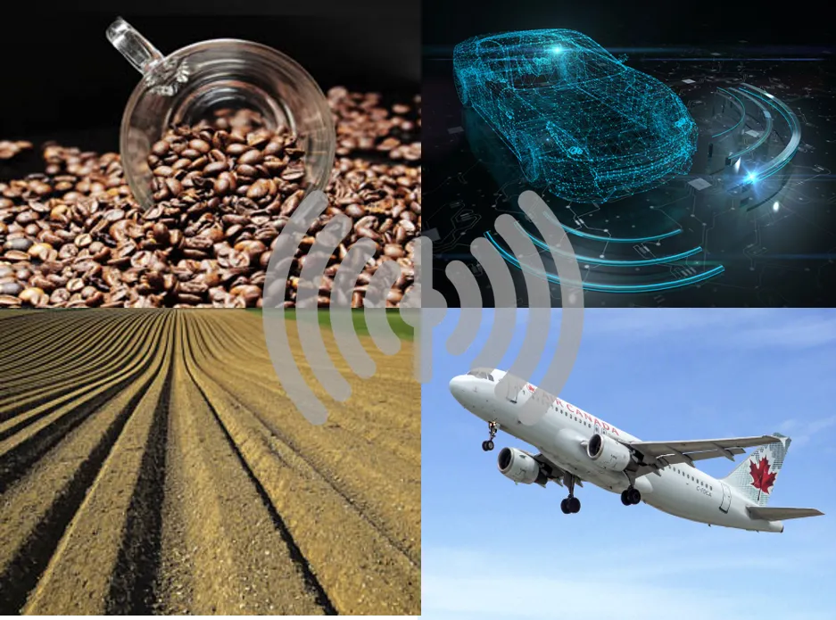
Part of 1 of 2-part series on MSEC 2019 highlights. Read Part 2. MEMS and sensors are proliferating across consumer, automotive, biomedical/healthcare, robotics, industrial and agriculture applications to harvest sensory data in a hyper-connected world and meet demand from consumers and organizations alike as they clamor for more intelligence in electronics.Take the ubiquitous iPhone. Shipped in 2007, Apple’s first iPhone sported five sensors. By contrast, the most feature-packed smartphones will embed up to 20 sensors by 2021, according to Yole Développement’s Jérôme Azémar. He estimates that the devices will feature four MEMS microphones, four CMOS image sensors (CIS), a RGB color sensor, a laser rangefinder, an infrared sensor, a gas sensor, a heart rate monitor and a fingerprint sensor, not to mention the MEMS inertial sensors that device users have come to know and trust.The MEMS market is expected to reach $18.5 billion in 2024 [1], up a whopping 60 percent from $11.6 billion in 2018, according to Azémar, who presented at MEMS Sensors Industry Group’s 15th annual MEMS Sensors Executive Congress (MSEC) in late October in Coronado, Calif. Add other types of sensors to the mix – CIS, environmental sensors, LiDARs, radars, ultrasonics, and fingerprint sensors – and the market will mushroom to $93 billion by 2024, said Azémar.Since MEMS Sensors Industry Group (MSIG) joined SEMI as a Strategic Association Partner three years ago, SEMI has expanded its MEMS and sensors programs to Europe and Asia while continuing to grow its U.S. conferences. “SEMI is continually investing in MEMS and sensors innovation across the supply chain,” said Dave Anderson, president of SEMI Americas and host of MSEC. “For example, MSIG is contributing to the development of the Heterogeneous Integration Roadmap, an initiative designed to drive heterogeneous integration technology development and accelerate electronics innovation. The roadmap spans device design, test and fabrication, ecosystem development, R D, equipment and materials. “At MSEC, executives and other speakers explored how AI and blockchain are remaking the food supply chain, air transportation and other sectors as MEMS and sensors improve the quality of our lives,” said Anderson.Sensing at the EdgeThe concept of artificial intelligence (AI), that a machine can harness intelligence that rivals or outperforms humans – and act without human intervention – has been a feature of the human imagination since at least the 1968 film 2001: A Space Odyssey. MEMS and sensors facilitate intelligence in a wide range of electronics such as smartphones, healthcare wearables, robots, industrial predictive maintenance systems, and cars. AI is sure to augment that functionality.MEMS and sensors are now in their third wave of evolution, a focus on edge AI, Bosch Sensortec CEO and General Manager Stefan Finkbeiner told MSEC attendees. For its part, Bosch is working to add AI to MEMS devices. The first wave integrated software with MEMS sensors, and the second, sensor fusion, enabled designers to allocate performance and power strategically to tune MEMS for resource-constrained devices. The third wave is “an active-learning phase in which MEMS facilitates real-time learning at the edge to promote greater personalization, environmental feedback, privacy of user data and improved battery life,” said Finkbeiner.Small sensor nodes with edge AI exemplify third-wave applications. Integrating low-power environmental sensors (e.g., gas, temperature, pressure, humidity and air-flow sensors), the nodes could be deployed in fire-prone forests to assess fire risk and support early detection. Access to this real-time environmental information could prove invaluable to residents and public-safety personnel alike.Google takes another tack, applying machine learning to resource-constrained devices, said Nick Kreeger, a senior software engineer at the Internet giant. The company’s Google Brain creates machine learning models that can run on inexpensive, low-power microcontrollers using Google’s TensorFlow Lite, an open-source machine learning tool that’s been deployed on a multitude of mobile devices. Inferencing is done at the device’s edge, rather than transmitted to the cloud.Meeting the power constraints of battery-powered sensing devices is another matter that starts with minimizing energy and data waste. “Deep learning is compute-bound and runs well on existing microcontrollers,” Kreeger said. “Because it’s all arithmetic, it’s low-power compared to storage access.”Already Google has worked with Plant Village, a research unit at Penn State University, and the International Institute of Tropical Agriculture (IITA) to help farmers improve food production by using machine learning and cheap sensors to spot and manage planet diseases in developing countries. And that production chain is in dire need of a boost, according to Rajendra Rao, general manager of IBM Food Trust, an enterprise-class blockchain solution.“We are on the cusp of complete failure of the food system,” Rao said. “One out of 10 people gets sick each year from foodborne illness, 420,000 die from this annually, 80 percent of companies in the food supply chain have not digitized, one-third of all fresh food in the US is thrown away, and one in five seafood samples worldwide is mislabeled.”IBM Food Trust’s work with Sucafina, which manages a global green coffee supply chain, shows how sensors can trace food from the farm to the processing plant to the consumer. With the IBM Food Trust platform, Sucafina can track the origin of the beans used in a cup of coffee – a competitive differentiator to coffee drinkers eager to support fair-trade coffee roasters.ripe.io, one of Forbes’ 25 most innovative AgTech startups, is also tackling the challenges and complexities of the food supply chain.“Our secure blockchain platform creates a digital twin of food items, transparently aggregating foods’ journey in real-time, to provide a harmonized trustworthy platform for multiple stakeholders,” said Rachel Gabato, the company’s COO. The ripe.io blockchain-based platform collects data from various sensors – temperature, pressure, light, humidity and inertial MEMS sensors. Growers, distributors and end customers including sweetgreen – a U.S. restaurant chain that depends on fresh produce – use the information to trace the origin and quality of food.MSEC 2020Mark your calendar for next year’s MSEC, October 12-14, at Coronado Island Marriott Resort Spa in Coronado, Calif. Get updates from MSIG on MSEC and other upcoming events including MSTC 2020.Stay in Touch with MSIGMEMS Sensors Industry Group (MSIG), a SEMI Strategic Association Partner, is the industry association representing the global MEMS and sensors supply chain. To learn how MSIG enables professionals in the MEMS and sensors industry to innovate, address common challenges and accelerate business results, visit us today.Connect with MSIG on Twitter and LinkedIn. Subscribe to SEMI Blog: Technology and Trends.[1] Source: Status of the MEMS Industry report, Yole Développement, 2019Maria Vetrano is a public relations consultant at SEMI.
Read More
Software for sensors has evolved from simply reading out and evaluating sensor data to making intelligent decisions based on that data, a transformation enabled by new software synthesis and artificial intelligence (AI) technologies. Together, they make consumer devices smarter, dramatically improving the user experience through greater interactivity and higher levels of automated personalization.SEMI’s Nishita Rao spoke with Stefan Finkbeiner, CEO and General Manager at Bosch Sensortec, who will explore the topic in his October 23 keynote, How Software Makes MEMS Sensors into Smart Systems, at MEMS Sensors Executive Congress (MSEC), October 22-24, 2019, at the Coronado Island Marriott Resort Spa in Coronado, Calif.Join us at MSEC to meet Bosch Sensortec and other industry influencers driving MEMS and sensors innovations. Registration is open.SEMI: What is the relationship between MEMS sensors suppliers and specialized software synthesis providers?Finkbeiner: Collaboration is a key driver for innovation in sensor software. There are already several fruitful collaborations between MEMS sensors suppliers and specialized software providers, which are mostly startups. Collaborations with providers of simulation and evaluation tools as well as with well-known universities in the field of AI are starting to show positive results.Domain expertise is also critical for developing smart sensor software, making it essential to future sensing solutions.SEMI: How does software synthesis relate to sensor fusion?Finkbeiner: Put simply, software synthesis refers to ways of automatically generating code based on domain knowledge and given constraints for specific product versions. Sensor fusion combines sensor data from different kinds of sources in order to improve the results.Software synthesis techniques enable a level of automation that creates new opportunities for more complex sensor fusion, which was formerly out of reach when using traditional approaches that involved, for example, big data and a large number of potential data sources.The traditional sensor fusion toolset can now be further extended by machine learning techniques that help to determine which sources are more reliable than others and how to combine data streams. This topic and others are still active areas of research. A wearable device with motion detection is a case in point. With unsupervised learning, the device could identify short versus long cyclically repeating motions and treat them differently from other types of motion. SEMI: How is the new software synthesis-AI approach different from previous approaches? To what degree will the new approach open up new applications?Finkbeiner: Traditionally, technology companies have used cloud computing for data storage and machine learning on aggregated user data. In that model, MEMS sensors generate large amounts of data that power-hungry hardware (such as digital signal processors) must process. In addition, machine learning generally requires lots of power-hungry cloud nodes with GPUs. This model, however, is not the best option for many users. Just think for a moment about all the scenarios in battery-powered devices where frequent battery charging frustrates users.Leveraging both software synthesis and AI techniques in MEMS sensors is therefore a very promising approach because it supports improved recognition and learning inside the sensor. This means that user-specific data isn’t transferred to the cloud. Instead, it remains private inside the sensor. This improves existing applications that learn all the time and opens up new opportunities for applications such as smart clothing, predicting a product’s lifespan, detecting whether a window or door is open or closed – all without server connectivity.SEMI: How will such software adapt to the individual user?Finkbeiner: Devices will offer much more personalized information to users. For example, optimizing a step counter to match the height, age or Body Mass Index (BMI) of a user – or to adapt to a user’s environment (is the person running on a beach, hiking up a mountain or strolling in a park?) – will provide more accurate information on calories burned. Not every step is created equal, and both pre-loaded personal data as well as real-world environmental data will prove that some steps consume a lot more energy than others.SEMI: What would you like MSEC attendees to take away from your presentation?Finkbeiner: I want to introduce the journey of software development by illustrating specific use case examples. I would also like to offer my outlook on the role of software and AI in MEMS sensors to help increase their adoption in current and new applications. Ultimately, I think it’s important to raise awareness in our industry on why we should embrace the use of software and AI.Connect with Stefan Finkbeiner at MSEC or via LinkedIn. Get more information on Bosch Sensortec products and solutions online.Stefan Finkbeiner, Ph.D., CEO and General Manager, Bosch Sensortec, was appointed CEO of Bosch Sensortec in 2012. He joined the Robert Bosch GmbH in 1995 and has been working in different positions related to the research, development, manufacturing, and marketing of sensors for more than 20 years. His senior positions at Bosch have included director of marketing for sensors, director of corporate research in microsystems technology, and vice president of engineering for sensors.Finkbeiner received his Diploma in Physics from the University of Karlsruhe in 1992 before studying at the Max-Planck-Institute in Stuttgart, where he earned his Ph.D. in Physics in 1995. In 2015, Finkbeiner received the prestigious lifetime achievement award from the MEMS Sensors Industry Group (MSIG), a SEMI technology community.Bosch Sensortec is a member of MEMS Sensors Industry Group, the industry association representing the global MEMS and sensors supply chain. To learn more about how MSIG enables professionals in the MEMS and sensors industry to innovate, address common challenges and accelerate business results, visit us today.Nishita Rao is marketing manager for technology communities at SEMI.
Read More
The semiconductor industry is in the final throes of its most recent cyclical downturn, but clear demand drivers on the horizon, such as 5G and autonomous driving, have created a decidedly upbeat mood at SEMI’s Strategic Materials Conference, held this week in San Jose, California. Increased connectivity in daily lives will not only dramatically boost semiconductor volumes, but the physical challenges of improving chip performance have positioned materials as the key enabling technology of the fourth industrial revolution – creating opportunities for suppliers to capture significant value. Most speakers were quick to underscore the importance of materials innovation. According to Dave Anderson, president of SEMI Americas, “We are entering the era of the material scientist,” and the role of materials in semiconductor manufacturing “has never been more important.” Carlos Diaz, senior director, corporate research at foundry major TSMC, said that the future “belongs to new materials and processes,” while Bertrand Loy, president and CEO, Entegris, told attendees the world is on the brink of the fourth industrial revolution, where technology will be fusing “physical, digital, and biological worlds and transforming our collective lives.” Len Jelinek, senior director/semiconductor manufacturing, IHS Markit, noted that 2019 has been a challenging year for semiconductor revenue – expectations are for a 12.5% decline YOY – but said he is not forecasting “doom and gloom” because of positive consumer demand trends beyond 2019. These include the rollout of 5G networks, internet of things (IoT), artificial intelligence (AI), and autonomous vehicles. Jelinek emphasized the foundational impact of 5G in particular. “Don’t think of 5G’s impact only in terms of handsets. It’s an enabling technology that will have broad-based impact” and will be key to creating a sustainable recovery in semiconductor demand in the second half of 2020. The current semiconductor downturn – the industry’s 10th – was initiated by an imbalance in memory supply and demand, and the lack of resolution of trade issues between China and the US is threatening to amplify volatility. Smartphones, the number-one application for semiconductors, are currently challenged by extended replacement cycles, and total handset shipments are set for its second year of decline. “We, as consumers, are waiting for revolutionary features such as 5G speeds, biometrics, foldable handsets and AI capabilities,” Jelinek says. Recent iterations have been merely evolutionary, and premium handset costs have escalated, he adds. Automotive electronics, which account for about 10% of global semiconductor demand, will eke out slight growth in 2019, Jelinek says. “Long-term semi component revenue growth within the Auto segment will focus on increasing content within cars supporting advanced safety features.” During his session, Duncan Meldrum, chief economist and founder of Hilltop Economics, addressed recent threats of a recession. “Underlying economic fundamentals are strong, but we are at that point in the business cycle where it doesn’t take much to knock the economy into recession,” he says. “I am telling people to have a contingency plan in place.” Nevertheless, Meldrum laid out reasons for optimism. Most economies have plenty of jobs, and consumers have been confident despite negative headlines. “For the average person, a tariff trade war gets to be noise. If they don’t see immediate impact, they tend to eventually discount all the headline noise. The same goes for Washington politics or Brexit.” There are no serious signs of inflation pressures in the US or other major economies, he adds. Beyond the cycleLonger-term, explosive growth in connected devices will create a runway for semiconductor volume growth. According to SEMI, over 30 billion devices are currently connected and another 200 million are added daily. By 2020, the number of connected devices will reach 1 trillion. “The growth profile for industry will be very strong and a multiplicity of drivers will bring more stability to this industry,” Loy adds. “But before this future becomes a reality we have a lot of work to do.” Current chips need to be faster and cheaper. “Physical scaling is not going to get us there, we’ve hit those limits,” Loy adds. “We have to look at new architectures and materials.” Loy called on the materials sector to need to “up our game” and spend more on R D. “Customers want us to make our products in very tight process window and ship to control. They want extreme purity for everything. It’s a long list of to-dos and it’s going to cost us a lot,” he adds. Among the needed innovations are photoresist hard masks to hand high aspect ratio, new etch chemistries for better rates and higher selectivity, and new cleaning chemistries for high aspect ratio geometry with high selectivity.Loy also identified contamination control as a key challenge for material suppliers. “When you think about purity and contaminants, you need to think about size, concentration levels, and classes. To optimize yields and lower wafer defectivity, our customers expect materials to be very pure and exhibit low variability.” The payoff for customers is large; a 1% yield improvement can mean $150 million in annual net profit for a leading-edge logic fab, Loy says. For a 3D NAND fab, that figure can be around $110 million per year. But these requirements are getting exponentially tighter. From 28 to 7 nm, the metal impurity concentration limit became 1,000 times lower, Loy notes. Contamination control is even more vital when the potential impacts of latent defects – which are difficult to detect in a fab and during electrical testing – are considered, particularly in emerging applications like autonomous driving, Loy says. “The cost of yield loss is expensive, but failure in a critical optical sensor of a car could be significantly greater, in terms of recalls or even human loss of life.” To meet tightening purity requirements, Loy recommends throwing out traditional thinking about contamination control. “In the past, we could get away with simple filtrations,” he says. “That’s no longer going to work. We need to collectively, up and down the supply chain, migrate to better filtration and purification and also rethink chemical delivery systems and packaging solutions to preserve the integrity of our products.”Metrology will also be key, but analytical capability is lagging. “We all like to believe that we cannot control what we cannot see, but that is exactly what we have to do.” The need for innovation is also being felt at the wafer level. Kevin Light, director, Applications Technology Americas at Siltronic Corp., said that as semiconductor markets become more diversified, silicon suppliers must recognize the distinct challenges each segment faces. Better wafer properties are required for next-generation chips, he adds. “Excessive wafer geometry can cause errors during lithography, especially when printing even smaller linewidths,” he says. The end result can be defocus and placement errors. When dealing with “More than Moore” architectures, wafer requirements are driven by other factors than defects. “More than Moore applications do not benefit from scaling, but instead drive capabilities of separate silicon parameters,” Light says. “In some cases you need high doping, in others the doping needs to be precise.” Czochralski crystal growth is suitable for high dopant levels, but the concentrations vary at the top and bottom of the ingot. Float Zone crystals avoid oxygen incorporation and provide consistent doping. These variations make Czochralski process suitable for PowerMOS, and Float Zone appropriate for IGBT. Compound semiconductor layers, such as GaN-on-Si, offer potential advantages owing to higher switching speeds and critical breakdown fields, he adds. “Silicon wafer requirements are diversifying as the devices themselves find increasing use outside of traditional logic,” Light adds. “Moore’s law is alive and next-gen computing will continue to push the limits of flatness and cleanliness. Meanwhile, demands of energy efficiency, electrification, IoT, and 5G drive wafer requirements other than scaling, including extremely high doped or ultra-low oxygen growing techniques, high lifetimes, and substrates engineered for compounds semiconductors.” Driverless futureAutonomous driving was a frequent discussion topic at SMC. Although IHS Markit does not see it really rolling out until past 2025, the disruption to the auto industry’s status quo is very much being felt now. Dragos Maciuca, executive technical director, Palo Alto Research and Innovation Center at Ford Motor Company, says cars of the future will be autonomous, connected, electrified, and shared. “The biggest transformation will be the shift from mechanical hardware to software,” he says. “Currently [a car] is a mechanical thing that has some electronics. Going forward, it will be a software-driven system that happens to control some mechanical elements.” The transition is already way under way, so much so that autonomous technology developed for the automotive industry is already being spun off into other sectors, such as mining and agriculture, and the auto industry’s competitive landscape is already seeing changes. OEMs and carmakers are entering the market from the traditional auto industry side, while companies such as Google are participating from the software side. “Others, like Uber and Lyft, are coming in from the business plan point of view to eliminate drivers and improve margins,” Maciuca adds. Autonomous driving will require numerous innovations, many of which will require new electronic materials and production processes. “We need weight savings, space savings, and advanced architecture,” Maciuca says. “We also need customization to print circuits as the vehicle comes down the line.” The tech community is proving up to the task. For LIDAR, there were just two technologies available a few years ago, he adds. The impact on chipmakers is also already being felt. “The automotive industry used to buy older chips,” Maciuca says. “Now we are moving to a stage where we need the very first chips at the most advanced node. And we are using them for safety-critical operations. If an AI chip that is supposed to detect a human fails, the consequences can be very severe.”Rebecca Coons is a senior editor at Chemical Week. Republished with permission from Chemical Week.The SEMI Electronic Materials Group (SEMI EMG) is the backbone of the Strategic Materials Conference. EMG is a technology community representing SEMI member companies that provide substrates, polymers, metals, organic and inorganic materials, chemicals, and gases that are developed or in use for the manufacturing of electronics. The group is open to SEMI Members involved in materials manufacture, distribution, and services throughout the microelectronics industry. For more details, please visit the website.
Read More
The evolution of industrial and non-industrial automation, smart manufacturing, and Industry 4.0 technologies have increased demand for vision systems that support robust, reliable imaging industrial applications. What factors are driving growth in the machine vision market today?SEMI spoke with Frederic Laune, Business Manager, European Technology, Corning, about how Corning® Varioptic® Lenses are vital to advancing the speed, efficiency, and integration of products using computer imaging. Laune shared his views ahead of his presentation at SEMI MEMS Imaging Sensors Summit, 25-27 September, 2019, at the WTC in Grenoble, France. Join us at the event to meet Corning and many other key industry influencing players. Registration is open.SEMI: Corning's markets include optical communications, mobile consumer electronics, display technology, automotive, and life sciences vessels. Back in June 2019, Corning Incorporated announced that it had delivered its 2 millionth Corning® Varioptic® Lens for industrial applications. What drove this great milestone?Laune: This milestone was met thanks to the fact that Corning Varioptic’s solution solves several problems generated by classical motorized solutions used in industrial applications: limited number of actuation cycles, poor vibration and shock resistance, size (meaning bulky), and high-power consumption. Before Varioptic, there was no variable focus solution that worked well.In addition, the explosion of the CMOS sensor technology helped drive down the cost of imaging solutions for industrial devices, increasing the number of applications and shipping volumes.SEMI: What inspired Corning Varioptic Lenses?Laune: Varioptic was started in 2002 by Dr. Bruno Berge, a French physicist turned entrepreneur. Inspired by the work of Gabriel Lippmann, the 1908 Nobel Prize winner for the invention of color photography, Dr. Berge explored the shape-altering effects of an electric charge when applied to two liquids, a phenomenon referred to as electrowetting. His research ultimately led to the creation of liquid lenses.Fast forward to 2017, when Varioptic became a part of Corning through an acquisition that included Varioptic and Invenios technologies. We believe the synergies from this acquisition will lead to exciting new liquid lens application opportunities that align with Corning’s growth strategy and core capabilities. Corning is one of the world’s leading innovators in materials science. For more than 165 years, Corning has applied its unparalleled expertise in glass science, ceramic science, and optical physics to develop products that transform industries and enhance people’s lives.SEMI: What differentiates traditional camera systems from adjustable lens solutions?Laune: Traditional industrial cameras are usually fixed focus, meaning that the image is sharp only in a limited distance range. Unlike consumer camera applications, there were no good solutions for variable or auto focus cameras in the industrial space. This is due to the intrinsic limitations of motorized technologies.Therefore, customers were using, for example, several cameras to focus at several distances. This compromises the optical quality by closing the objective in order to increase the depth of field, therefore limiting resolution and leading to a need for more light.The cameras using Corning Varioptic’s technology offer more functionality with their ability to focus, whatever the distance, in a fast, reliable, and accurate fashion, and with lower power consumption than traditional mechanical solutions. The upshot is that the product that can withstand heat, vibration, mechanical shocks, and high numbers of focus cycles in tough industrial environments. SEMI: And how is electrowetting enabling industrial devices to capture images and process information quickly and clearly? Laune: In two words: fast and accurate.Electrowetting has unique features – with our two-liquid solution, we combine fast focus with high vibration and shock resistance, and the added benefit of low power consumption.What’s more, our programmable lens can be reconfigured on demand. The lens adapts rapidly and continuously from diverging to converging and can be modeled to support demanding variable focus applications. Our lenses can change their focus in milliseconds, similar to the human eye, and capture fast-moving objects at varying distances. The use of liquid, over mechanical solutions, allows us to create a small form factor, saving precious space and reducing power consumption.SEMI: What industrial applications are taking advantage of this technology? Can you name one example?Laune: 2D barcode readers and industrial vision are our main markets. There is also a strong adoption of our technology in medical applications.SEMI: What does the rise of machine vision mean for manufacturers? Give us one prediction about the opportunities offered by advanced imaging applications.Laune: A great example is the use of 2D barcode readers and liquid lenses to track your ecommerce order, point to point. Another example is full product traceability by implementing a 2D barcode on every component of a given product globally to improve product quality. The varying and adjustable focus abilities of our liquid lens technology make it possible for barcode scanners to track products of different heights, allowing manufactures to improve their processes and logistics.Beyond these examples, tracking and analyzing are booming, thanks to the combination of low-cost CMOS sensor technology, increasing processing power, innovative algorithms (deep learning, AI, neuromorphic processors, etc.), and better image quality due to the progress of lens technology, Varioptic being one.We see an opportunity to improve people’s lives, such as enabling better analysis of medical images and improving the use of cameras in biomedical technologies.SEMI: Quality inspection and automation, adoption of Industrial 4.0 technologies, government initiatives. If you were to choose one, what main factor will drive growth in the machine vision market?Laune: It is difficult to pick just one. I believe that full traceability (monitoring individual parts throughout the production process) has interesting implications as compliance and regulatory efforts ramp up and stronger security of goods becomes more important, particularly as consumers become engaged in food safety and tracing products throughout the supply chain.SEMI: What are your expectations for the SEMI MEMS Imaging Sensors Summit and why would you invite your peers to attend? Laune: I strongly believe in the power of human interactions in technology and science! Ideas come from discussions and physical interactions. The SEMI MEMS Imaging Sensors Summit is a great place to network, meet people, and think about the future! Frederic Laune is the business manager leading the Corning® Varioptic® Lenses business. Laune joined Varioptic as an R D engineer in 2003 after spending the first eight years of his career developing novel active components for the optical telecom industry. At the time, Varioptic was a newly created start-up aiming to develop liquid lens technology for industrial applications. After designing the first two Varioptic commercial products, the Arctic 320 and Artic 416, Laune stepped up as head of Varioptic’s R D department to focus on product and performance improvements. In 2010, he was appointed sales and marketing lead for the company. Varioptic was acquired by Corning Incorporated in early 2017. Laune received a master’s degree in physics and optics from University Pierre and Marie Curie (Paris) in 1995.Serena Brischetto is a marketing and communications manager at SEMI Europe.
Read More
This article is the fifth and final in a series highlighting the vital importance of SEMI Standards to commemorate the publication of the 1000th SEMI Standard in July 2019. Find the entire series here.As we define industry standards for managing data in the fab and beyond, we are creating a virtuous circle. More data create better processes. Better processes generate more good data, and more good data lead to better processes. It becomes a cycle of continuous improvement, and we are only just beginning to realize its potential. To dive deeper we interviewed Alan Weber, vice president, New Product Innovations at Cimetrix, and an active member of SEMI Standards Information and Control Committee (IC C).“Industry standards are critical in allowing us to collect information across the fab and use it in increasingly sophisticated control algorithms for the equipment,” said Weber. “The last few years have been about analysis applications that leverage big data in the fab. What started at the lot level is now applied at the wafer level, and for a process like lithography, it’s down to the shot or die level. We’re now collecting enough data variables at individual process and recipe steps to model for predictive maintenance and virtual metrology.”The migration from using data as rearview mirror for identifying and addressing fab issues to using data to head off issues preemptively represents a paradigm shift with immense advantages. This is the starting point for realizing a virtuous data circle.The benefits of a virtuous data circle are simple and compelling: higher yields, faster time to market, more revenue and greater profitability. Our optimism, however, is tempered by major obstacles to this promising future.Multilingual ManufacturingWeber points out that the electronics industry is becoming a multilingual standards world with more than 1,000 fab equipment vendors and several layers of protocols that present the challenge of seamlessly handling multiple protocols. His IC C Committee is out to tackle this challenge.“While SEMI Standards efforts first began in the front end, our standards program now encompasses the back end with test and packaging as well as other device areas including MEMS, sensors and displays,” said James Amano, senior director, International Standards and EHS, SEMI. “We’re going to see data connectivity from the front end to the back end to the final assembly of multi-chip products and that needs standards,” Weber explained. “We’ll need more connected equipment throughout the global, multi-site manufacturing process if we are to support the full traceability requirements of the most demanding markets such as automotive.”The industry will benefit from greater collaboration. Weber predicts that companies will team to create integrated supply chains within broader industry supply chains.Getting the Right People at the Right Time“As we lead the development cycle of a standard from concept to realization, one of the most important jobs of our standards task forces and committees is to coordinate competing companies and build an industry consensus,” Amano said. “This is the case for data in particular, where we rely on industry professionals like Weber and his colleagues, who are working to bring people together to collaborate on developing standards for connectivity and data sharing. It is that critical human element that allows SEMI to sustain our commitment to introducing standards that move the industry forward.”Will Companies Share Data If It Is Secure? Weber contends that when it comes to securing and sharing the data, the biggest challenge is to change the industry’s information-sharing culture.“Finance and defense are already finding ways to deal with data security,” said Weber. “While we will always have problems that require technology fixes, like dealing with new types of computer viruses, I am confident that we will be able to create standards that enable the free, secure flow of information. The key to making progress and better leveraging data is to get companies to see the potential of sharing data while investing in the standards.”SEMI recently launched a project to optimize data sharing across two critical process steps – lithography and plasma etch – to accelerate the adoption of data-driven AI methodologies. The results will help to establish data transfer and management standards crucial to the trusted exchange of trade secrets, IP and other sensitive information. Tools and materials from several SEMI members will be used for the project at Cornell University’s NanoScale Science Technology Facility (CNF). SEMI members are invited to join the project review team. Contact Pushkar Apte at SEMI ([email protected]) for more information on the initiative.Advantages Are Too Great to IgnoreTraditional cultural obstacles aside, the advantages of creating virtuous data circles are simply too great to ignore. Now that it’s accepted wisdom for fabs, factories and supply chains to continuously leverage interconnected data to get smarter, the time has come to extend those advantages throughout the full manufacturing process. Without these data circles, we’ll slow the development of new technologies and applications.We can only speculate where the lines of sharing data are drawn and will be redrawn in the future. But, without doubt, technology innovations such as AI will spawn new information business models that vertically and horizontally integrate companies in ways previously unimaginable. Data standards will underpin this structural transformation.Use your voice to affect standardization in and around the microelectronics industry. Learn about SEMI International Standards – and become part of the solution. Heidi Hoffman is senior director of technology communities marketing at SEMI. Hoffman and her team shine a spotlight on the work of the more than 20 technology communities under the SEMI electronics manufacturing supply chain collaboration platform. Actively engaging community members in marketing programs that showcase their unique value, Hoffman’s team helps companies to grow and prosper through the power of connection, collaboration and innovation.
Read More
AI vs. energy. Quantum for everyone. Biofabrication of human organs on a mass scale. Slowing advancements from Moore’s law.In the midst of a market dip, optimism reigned as keynote and AI Design Forum speakers addressed both looming challenges and explosive market opportunities during July 9-10 presentations at SEMICON West 2019 in San Francisco. SEMICON West again proved to be a magnet for visionaries who laid out the path to electronics innovation over the coming years.“The current business environment demands that the industry looks ahead toward issues that need attention sooner, not later – especially since we are approaching a once-in-a-generation inflection point that has the potential to be a $10 trillion opportunity,” observed SEMI Americas president Dave Anderson.Market forecasts punctuate the point: The microelectronics supply chain is on the verge of what has the potential to be the longest-lived electronics era.“Inflection points like this are rare, but not unprecedented,” Anderson added, citing 2007 as the inflection of the growth curve from new technologies that led to last year’s historic high semiconductor sales.SEMICON West squarely focused on the future, with a number of industry leaders noting that chip, tool and materials makers need to look beyond their immediate suppliers and customers in developing strategic partnerships. Dr. Cliff Young, data scientist with the Google Brain Team, for one, invited semiconductor and equipment firms to explore chip codesigning opportunities with his Google.The recently formed Quantum Economic Development Consortium – and its 50 members including Boeing, Google and IBM – debuted roadmapping activities devoted to the pursuit of U.S. leadership in the rapidly emerging global quantum computing industry. IBM’s Jeff Welser showcased the IBM Q Computer model built upon decades of semiconductor industry advances. Markets that could see staggering leaps from a quantum computational capacity include automotive, medical, financial and energy. Today, anyone can dabble with the future quantum computing capabilities by connecting online with IBM’s 16-qubit quantum computer. Dr. Aart de Geus, chairman and co-CEO of Synopsys, suggested that software and other programming tends to develop more quickly if it is open sourced. He recommends an open source model that allows semiconductor and equipment companies to work together in the cloud to speed chip development.Nate Baxter, TEL development and production group general manager, advocated sharing big data with competitors in pre-competitive spaces to ensure data quality, improve measurement and solve problems faster. The key is security. “Yes, we can share data while protecting it,” he said. “We’re quickly seeing opportunities that we didn’t know existed.”Gary Dickerson, Applied Materials president and CEO, said that embedding artificial intelligence (AI) in chips will drive significant long-term industry growth by processing far more big data computations much faster than humans can.That is, if there is enough electricity. Almost invisibly, AI-enabled machines already are crunching massive amounts of data while gulping power in the process. As AI use rapidly expands, current power grids will be stressed as never before. Dickerson added that speed of innovation, societal acceptance, security and safety will guide how well and quickly AI is adopted. A potential hurdle, however, is sustainability. He warned power constraints could be “very high” and a “barrier to AI adoption if we don’t drive innovation” in substantially reducing the power draw of power-hungry AI chips.Of the five members of a venture capitalist panel, four agreed that Moore’s Law as we knew it is dead. The promising news is that the average age of a first-time mobile phone user is 10, more than 40 percent of the world population is now under 25 and about to wield considerable market influence, and 5G is on the cusp of helping connect trillions of devices. AMD CEO Lisa Su noted “there’s a tremendous amount of innovation yet to come” from microarchitectural advances, chiplets and die stacking, and heterogenous platforms.And there’s nothing more innovative – or intriguing – than regenerating human organs in mass volume. Legendary inventor Dean Kamen laid out his well-funded plans to biofabricate the viscera of human existence but warned of two crucial missing pieces – scale and talent. “I’m here at SEMICON West to beg for high-tech’s help in getting artificial human organs out of labs and ramped up for volume manufacturing and widespread distribution,” Kamen said during his keynote. “The basic science already exists, but researchers can’t bring it to scale like Silicon Valley can.”The talent Kamen needs to fulfill his dream will come from the pool of skilled workers the microelectronics industry is feverishly working to recruit to make good on its own ambitions. As if on cue, SEMI endorsed Kamen’s FIRST Global program, establishing a united effort to encourage young people worldwide to pursue engineering careers. “Together, we can better help provide a path to success for generations to come,” SEMI’s Anderson said.Scott Stevens, SEMI
Read More
New system-on-chip (SoC) devices are driving new memory architectures and photonic interfaces, while specialized new intellectual property (IP) requires analysis down to the nanometer and atomic levels because of single nanometer process nodes. According to Babak Taheri, CTO and EVP of products at Silvaco, a leading EDA Software, semiconductor IP company, a member of SEMI and the ESD Alliance, a SEMI Strategic Association Partner, design technology co-optimization and proven IP are required for this analysis.Taheri recently discussed atoms to systems in next-generation SoC designs with Nanette Collins ahead of ES Design West, co-located with SEMICON West, July 9-11 at the Moscone Center in San Francisco.ESD Alliance: For years now, the assumption is that each new chip design is more complex than the last. Why are the latest SoC designs even more complex than before?Taheri: New SoC devices for mobile phones, automobiles, intelligent edge nodes, big data compute and storage are adopting artificial intelligence and machine learning technologies. This is driving new compute, data flow, as well as memory architectures that are bandwidth-limited and some require photonic interfaces.One common denominator in present SoC design are the numerous blocks of IP. On average, over 85% of these blocks are reused. It’s cost-prohibitive to make these chips over and over again with new IP. According to some estimates, 90% of IP used in an SoC design by 2025 will be reused – only 10% is new technologies. That 10% is significant.ESD Alliance: How so?Taheri: Complex new technologies including flash memory, other advanced non-volatile memory technologies such as MRAM, RRAM and SoCs such as NVIDIA’s Xavier and Apple’s A12 use and reuse design IP at the architectural level.New technologies mean new materials and new processes. Single nanometer process nodes require specialized new IP that needs to be simulated and analyzed down to the nanometer and atomic levels.ESD Alliance: Does the atomic level changes the design equation?Taheri: Yes, it does. Designers need to be able to simulate at the atomic level and understand properties of these materials, and how they behave in at-process and at-device levels. They need be able to simulate the material's nanometer geometries, how molecules behave and how they interact for device operations. When they put together a process and a device, they need to know how the pieces behave and simulate before production.In other words, they run quite a few design experiments and quite a bit of simulation before they finalize the circuits and devices to silicon to save money.ESD Alliance: It’s obvious design automation will continue to have a vital role in design.Taheri: Yes, absolutely. Design technology co-optimization (DTCO) using TCAD solutions and proven design IP are needed to address the span from architecture to device and process physics. The importance of simulation, emulation and design technology co-optimization, along with fully verified and proven IP for SoC design, cannot be overstated. As designers generate devices and processors, they take that up to circuit-level simulation and high-level simulation, schematic capture, extractions and back annotation. They can go from atoms to simulating systems to the ability to do that under the same umbrella in order to get better chips, better yield and lower cost.Taheri’s talk Next Generation of SoC Design: From Atoms to Systems will be part of the Meet the Experts More than Moore session Tuesday, July 9, at 11:30 a.m. at the ES Design West SMART Design Pavilion. SEMICON West attendees are invited to Moscone Center’s South Hall to learn more about electronic system and semiconductor design and its links to the electronic product manufacturing and supply chain. Register for ES Design West or SEMICON West.Babak Taheri is Silvaco’s CTO and EVP of products, has more than 25 years of design experience. His current role managing Silvaco’s Technology CAD (TCAD), electronic design automation (EDA) and IP product divisions makes him an expert on what’s needed for the design of next-generation system-on-chips (SoCs). Previously, he was the CEO and president of IBT working with investors, private equity firms, and startups on M A, technology and business diligence. Babak received his Ph.D. in biomedical engineering from the University of California Davis with Bachelor of Science degrees in Electrical Engineering and Computer Science and Neurosciences. He has published more than 20 articles and holds 28 issued patents.Nanette Collins is a public relations representative for the Electronic System Design Alliance.
Read More