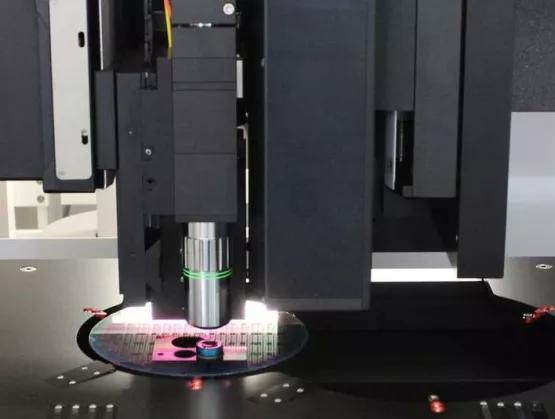
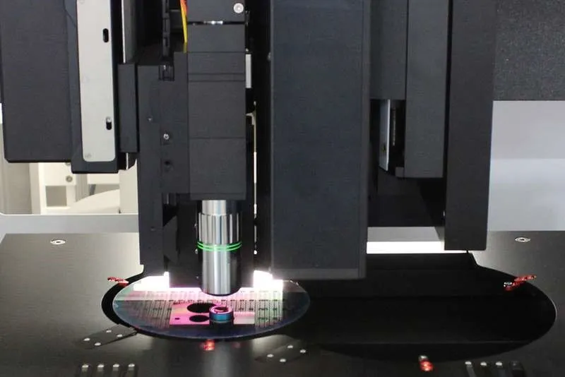
SEMI spoke with Thomas Fries, founder and CEO of FRT GmbH, about how hybrid metrology is shaping multi-sensor metrology tools to enhance measurement precision as the industry moves away from a single-sensor approach.Fries offered his views ahead of the SEMI MEMS Imaging Sensors Summit, 25 to 27 September 2019 in Grenoble, France. Join us at the event to meet experts from FRT Metrology and many other MEMS, imaging and sensors companies. Registration is open. SEMI: Metrology in front-end used to be straightforward. But then, as the number of tasks to be implemented increased, we moved to a multi-sensors approach. What drove this transition?Fries: I believe it´s more about software than about sensors. But of course the basis is the hardware. So, most metrology tools were designed around a specific sensor, e.g. a white light interferometer.A rigid frame, wafer fixtures, scanning tables etc. were then added to develop a complete system. In manufacturing more machinery was added, like handling systems, cleanroom equipment and more sensors, mainly for additive functions such as reading IDs or measuring temperature. The center was still the one and only sensor, being pimped more and more by some hardware features and a lot of software.SEMI: How are sensors and software shaping the way metrology is applied today?Fries: Today a huge number of optical sensors are available to provide various measurement options. But sometimes there are only very slight differences from one sensor to the other. A tiny variation may determine whether we solve a problem or end up fishing in troubled waters.And of course using different machines with those sensors requires high budgets for capital investment, used floor space, measuring time, etc. A multi-sensor platform solves all these problems. But again, it is the software that makes the real difference.SEMI: What lead to those advancements in metrology? What problems did they set out to solve?Fries: Metrology has been evolving ever since the measurement standards were established. The first challenge was to create a flexible mechanical platform that was also reliable and stable. All components were designed to be integrated into one system, mechanically, electrically and of course in the software.This level of integration requires not only an appropriate user interface, but also data formats and evaluation algorithms that leverage multi-sensor hardware. Today every metrology tool in the fab is justified by the application, not by specific sensors or specs. Of course the application leads to a set of specs, but the solution for the metrology task is realized within the software.New developments in metrology combine expertise in system design, physical knowledge in metrology and materials, mechanical engineering and also mathematical and software skills.The last step was the implementation of hybrid metrology functionality into a multi-sensor system that opens totally new doors in metrology. Before multi-sensors development, quite a few hitches could not be properly solved. SEMI: This is especially true when we consider applications in advanced packaging and MEMS manufacturing. What is in your opinion the main challenge?Fries: Specifically, in MEMS and advanced packaging we face multiple metrology challenges, as various processes run in one step and conditions on the wafer may vary quite often. In this case, a high degree of flexibility, up to the option to upgrade the metrology tool at any time or place, is a priceless advantage. Besides, cost effects for footprint, throughput and investment play a key role.A central task for nearly every customer application is to combine global measurements (complete wafer) and local measurements (per die) within one recipe. This is a perfect case for a multi-sensor platform. Measuring step heights and film thickness in one take is also an everyday routine. Combining those characteristics to measure hidden structures (hybrid metrology) is unique.SEMI: How will hybrid metrology enhance measurement precision and where do you expect the multi-sensor approach to be more applicable?Fries: The first advantage is the ability to measure properties that you cannot access directly. On top of that, all the previously mentioned features such as facing multiple metrology tasks, the combination of complete wafer and per die measurement are playing key roles. The precision of specific measuring tasks can be optimized by calibrating sensors against each other or combining results to get rid of noise or artefacts.MEMS and advanced packaging are natural playgrounds for hybrid metrology. But already today we see applications in high volume manufacturing in the 300mm fabs. As structures on wafers shrink, wafers are getting thinner and the whole process is becoming more and more complex. The classic one-sensor metrology tool is running out of gas. SEMI: What are your expectations regarding the summit in Grenoble, and for the future of the MEMS Sensors technology?Fries: FRT has always been very strong in MEMS and sensors and we have attended and exhibited at the SEMI MEMS Imaging Sensors Summit from the very beginning. The summit is always a very good meeting point for the community, and a perfect training session that gives participants extended updates in all fields. And of course, it grows our network and gives us the opportunity to show our latest products and applications.If you really want to know how the future of MEMS and sensors will look like, join the summit and don´t miss the chance to pass by the exhibition to meet FRT and many other industry leaders.Dr. Thomas Fries lives with his family close to Cologne. He is engaged in a variety of activities: as technical advisor to various ministries, supervisory board of PlanOptik AG, board and advisory board of IVAM, board member of COPT.NRW e. V., just to name a few. FRT supports many social projects as well as kindergartens and schools. Motorcycles and cars are still a great passion alongside his family.Serena Brischetto is senior marketing and communications manager at SEMI Europe.