downloadGroupGroupnoun_press release_995423_000000 copyGroupnoun_Feed_96767_000000Group 19noun_pictures_1817522_000000Member company iconResource item iconStore item iconGroup 19Group 19noun_Photo_2085192_000000 Copynoun_presentation_2096081_000000Group 19Group Copy 7noun_webinar_692730_000000Path
Skip to main content
Default Banner Image

VeriSilicon

Lots of great information came out of the two days of workshops in Japan recently organized by the SOI Consortium. Some of the presentations are now posted on the consortium website (get them here). The first day (held in Yokohama and sponsored by Silvaco) focused on FD-SOI and RF-SOI design. The second day (held at U. Tokyo) focused on More than Moore (especially silicon photonics, MEMS sensors), and the SOI manufacturing ecosystem. The 1st day panel discussion was so interesting we'll give it a post of its own, then follow up with round-ups of the presentations from both days. And now to ramp! The morning panel discussion on end-user deployment for FD and RF-SOI was moderated by SOI Consortium Executive Director Giorgio Cesana. GF's CTO Subi Kengeri led off saying that that 2017 had been the year of FD-SOI adoption. Samsung Director Adam Lee noted that in the beginning nobody believed it would get traction, but now everybody does, and Samsung is commercializing it: chips coming out this year will ramp in volume in 2019. [caption id="attachment_12578" align="aligncenter" width="875"] Panel on FD-SOI and RF-SOI end-user deployment, SOI Workshop Japan, 2018. Giorgio Cesana, SOI Consortium Executive Director, Moderator; John Carey, ST Director; Adam Lee, Samsung Director; Subramani Kengeri, GF CTO; Wayne Dai, VeriSilicon CEO; Mostafa Emam, Incize CEO. (Courtesy: SOI Consortium)[/caption] VeriSilicon CEO Wayne Dai said he sees great potential in IoT, where the volumes are high but fragmented. In IoT, he said, you need RF, but you really only need very high performance about 20% of the time, which is a perfect fit for FD-SOI. ST Director John Carey noted that ST's been using FD-SOI since 2014. They've fabbed products for cryptocurrency and infrastructure. Now in their second and third generations of designing with it, they've got some big FD-SOI chips coming out next year with embedded memory and RF. He sees it being particularly successful in mmWave, automotive and IoT. The conversation then shifted to RF-SOI. Mostofa Emam, CEO of Incize, explained that since RF-SOI is already in every smart phone, it's in a different situation from FD-SOI. The emphasis here is now on adding more blocks. “RF is an art,” he said. “It takes an artist. You need talented artists and tools.” One of the biggest challenges for fabs that are newcomers is models – not just at the transistor level, but also at the substrate level. The big players have addressed this, but Incize is working to support more foundries with new, innovative approaches, and helping them develop robust PDKs. The industry needs more good RF designers as well as better RF design flow, he concluded. Coming back to FD-SOI, Cesana asked about non-volatile memory (NVM). Samsung's Lee said they've already got NVM options including eMRAM for 28nm, and customers are now requesting eMRAM PDKs for the next node (18FDS). ST's Kengeri added eNVM is important for FD-SOI, especially since flash is not scaling. While there are lots of options, MRAM gives you all the value, and in FD-SOI it only adds three more mask steps, so cost savings are maintained. With respect to local computing for AI with FD-SOI, everyone agreed on the importance of the edge. In addition to RF, FD-SOI gives you density even at 28nm, explained Carey. You can manually control power with back biasing, so you get something very flexible, especially for NB-IoT applications where the battery will have to last for 10 years. In fact Kengeri sees FD-SOI as enabling fog/edge computing. 5G – What's First? The next question was about 5G: which applications would we be seeing first, and how does FD-SOI help? Lee said Samsung's seeing it for apps up to 10GHz as well as mmWave. Customers are telling them they want FD-SOI for technical reasons. Kengeri expanded on that point, saying it comes down to fundamental physics: gate resistance, capacitance, mismatch. FD-SOI has lower Vmin and better Fmax compared to FinFETs, and that's what tier-one players want. Carey brought it back to RF-SOI (noting that ST's introducing a 45nm version), which supports a large number of elements and increased complexity with smaller power budgets. Emam then asked the foundry guys about mmWave. Substrates won't be the bottleneck he said, so what's the FD-SOI/mmWave roadmap? Kengeri responded that GF's ready. Lee said Samsung is also ready, and you'd see it next year on handsets. Samsung has engaged with customers on 30GHz for the middle of next year, he added: it's qualified. Carey said ST sees it first in consumer premises equipment that's connected by satellite. The right enabler Cesana then asked about image sensor processors (ISPs), noting that analyst Handel Jones has said this is a big opportunity for FD-SOI. You can do 3D integration with sensors, but heat makes noise, so you need technology that decreases heat production and doesn't give you hotspots (which would be visible in the image). Kengeri pointed to challenges in power density, thermal envelopes and the RTS (random telegraph noise signal). Although there are a lot of options, FD-SOI plays well for thermals and noise, so GF sees a good opportunity here. Dai added that the industry needs volume applications for FD-SOI, and ISPs need to bring more logic closer to the camera. And he concurred that you need FD-SOI for the thermals: it's very important. In closing, Dai noted that as a design house, “We walk on two legs: FinFETs and FD-SOI.” 28, 22, 18 and 12nm FD-SOI all enable differentiation. In particular, you need something between 20nm and 7nm: FD-SOI is here. Asked about Japan in particular, Dai said beyond automotive he saw lots of potential in ULP for AVR. Kengeri added that for any applications besides performance-at-any-cost, FD-SOI is the right enabler.
Read More
Since about a third of all IoT devices are expected to be connected by Bluetooth, chip designers need IP solutions that will help reduce system cost and greatly improve battery life. And that's just what VeriSilicon has announced for GlobalFoundries' 22FDX® (FD-SOI) process. “By taking advantage of integrated RF capabilities of FD-SOI, in particular GF’s 22FDX, our BLE 5.0 RF IP will significantly reduce the system cost and greatly boost the growth momentum of wearable products such as wireless earplugs,” said Dr. Wayne Dai, Founder, Chairman, President and CEO of VeriSilicon. 22FDX enables efficient single-chip integration of RF, transceiver, baseband, processor, and power management components. GF and VeriSilicon are working on an SoC using VeriSilicon's BLE 5.0 RF IP in GF’s 22FDX process. The latest iteration of Bluetooth is 5, which (like its predecessor 4) has a Low Energy (LE) RF option – but with big improvements. According to the Bluetooth website, “With 4x range, 2x speed and 8x broadcasting message capacity, the enhancements of Bluetooth 5 focus on increasing the functionality of Bluetooth for the IoT.” BLE 5.0 was designed for very low power operation and is optimized for the sorts of short burst data transmissions you'll get with IoT. On the strength of VeriSilicon’s innovative RF architecture and by leveraging GF’s 22FDX technology, VeriSilicon says the new IP product achieves significant improvements in power, area, and cost compared to current offerings, so it will better serve the emerging and increasing wearable devices and IoT applications space. "VeriSilicon's BLE IP complements GF's 22FDX FD-SOI capabilities and is well positioned to support the explosive growth of low-power IoT and connected devices," said Mark Ireland, vice president of ecosystem partnerships at GF. "Together, we broaden our IP and services to further enable our mutual clients to provide power and cost efficient solutions." VeriSilicon BLE 5.0 RF IP includes a transceiver that is compliant with the BLE 5.0 specification and supports GFSK modulation and demodulation. The silicon measurement shows that the sensitivity can be tested up to -98dBm with less than 7mW power dissipation in typical conditions. It largely improves battery life for low power IoT applications. In addition, the RF transceiver saves 40% area compared to a similar implementation on 55nm bulk CMOS. Besides the RF transceiver, this IP integrates on-chip balun, TX/RX switch and 32K RC OSC driver to save the BOM. Moreover, high efficiency DC/DC and LDOs are also available for power management. You can read the full press release in Chinese here and in English here.
Read More
Excellent news and exciting applications made headlines at the recent FD-SOI and RF-SOI events in Shanghai. During the FD-SOI day, Amazon/Blink and Intellifusion shared news about their new chips, and we got updates from GF and Samsung. The RF-SOI day featured a great talk with details about China Mobile's 5G plans, and peeks at Nokia's groundbreaking approach and Qorvo's outlook. [caption id="attachment_12354" align="alignright" width="300"] (Photo courtesy: Verisilicon)[/caption] The hall was absolutely full – with over 300 people attending each day. The FD-SOI event was by invitation only, and there were far more people wanting to attend than there was room for, even given the big room in which the events were held. The events got excellent coverage in the China tech press. For example, EEWorld started with an overview article and added five supporting pieces zooming in on key presentations and companies: one on GlobalFoundries, one on Samsung, one on Verisilicon, and two on Soitec (CEO and top exec interviews). These pieces are in Chinese, but just open the links through your favorite translation site. Many of the key slides are captured in these articles, so if you can't wait for the ppts to be posted on the SOI Consortium website, you can get some quick previews now. The Verisilicon PR folks also wrote up highlights of the FD-SOI event in real time with lots of great pictures – you can read that here. Many thanks to that team, too, for flagging the coverage in the China press and posting it on their WeChat account. On the RF-SOI side, the Simgui folks wrote that up – you can read it here. They also sponsored a gala dinner with awards given to Qorvo and SmarterMicro – you can read about that here. Most of the presentations will be posted on the SOI Consortium website over the next few weeks, at which point we'll cover them in-depth here at ASN. But for now, here's a quick round-up of some of the highlights. FD-SOI Highlights [caption id="attachment_12347" align="alignright" width="300"] (Courtesy: Blink, Verisilicon)[/caption] Boston-area based Blink, which makes very popular home security systems, was recently bought by Amazon (see their current product page here). They just taped out a new chip on Samsung's 28FDS FD-SOI technology, and they're really happy about it. “I believe for battery powered devices at home, FD-SOI is the way to go,” said Yantoa Jia, Head of ASIC China Ops at Blink. Their goal in the move from 55nm bulk to 28nm FD-SOI was to double battery life, add features and control costs: and they did it. Even adding two more CPU cores and lots more features, “The power drop is fantastic,” he said. Design was no problem, he continued, and there was plenty of IP. Once the new generation is officially announced, he promised to sit down with ASN and give us more details. Attendees also heard about a new chipset from Intellifusion, which is putting its face recognition technology onto GlobalFoundries' 22FDX FD-SOI with design house Verisilicon. CEO Nin Chen gave an impromptu talk about how their technology is used to find missing people and property. The new chip, which is especially designed for use in cities, is network-to-cloud leveraging AI. For his part Thomas Morgenstern, GlobalFoundries SVP and GM of the Dresden Fab 1, said they're seeing high yields and increasing capacity for 22FDX. The marketing and manufacturing ecosystem has been built around the fab in Europe. Now, he said, the key is to build an FD-SOI ecosystem in China. The market needs of China largely parallel those of Europe, he noted, for performance and efficiency at the right cost point. The ecosystem enables fast time-to-market and 1st-time-right. [caption id="attachment_12343" align="alignleft" width="300"] (Photo courtesy: Cadence)[/caption] Samsung SVP Gitae Jeong sees their FD-SOI technology as the right solution for the 4th Revolution, which includes everything from energy harvesting to self-driving cars. They've just taped out their first 5G mmWave cellular chip on 28FDS, he revealed. eMRAM is looking very good, only requiring three additional masks and getting stable yields from -40o to 105oC. 18FDS is on schedule, with PDK 0.5 now being released, and 1.0 on track for release in March 2019. They expect a very fast ramp, and are looking at a 35% area reduction, power cut in half and performance up 22% compared to 28FDS. RF-SOI Highlights [caption id="attachment_12350" align="alignright" width="300"] China Mobile, Project Manager Danni Song (Photo courtesy: Simgui)[/caption] When China Mobile talks, the world listens. Project Manager Danni Song presented again this year (she gave a great talk last year, too). China has a very ambitious 5G project underway, and under two years in which to roll it out. The biggest challenges are power consumption and cost (a problem made worse by the additional power amplifiers needed for MIMO). Can RF-SOI help solve these challenges, she asked? One thing she did clarify during the panel discussion was with respect to the mmWave part of the 5G puzzle. Their initial 2020 rollout will only focus on sub-6GHz, with mmWave following a year or two later. Michael Reiha, Head of RFIC R D at Nokia Mobile Networks clarified the worldwide 5G rollout during the panel discussion. Different locations on the planet have different histories and needs, so will rollout 5G in different ways. For historical reasons (and a lack of choice), the US will lead with mmWave, he said. Europe, meanwhile, will focus on 24GHz to meet the needs of automotive radar. In his presentation, Reiha described Nokia's approach to power amplifiers (PA), which is very different from what others are doing. With RF-SOI, he said, you can add sensors and logic for a level of preventative care, so you can gauge and protect your equipment using AI. He believes this disruptive approach will put them two years ahead of the industry, enabling massive MIMO to be deployed in dense urban areas with 60% lower power consumption and 50% savings in material costs. Go read about their Reefshark tech, he urged, which he says will beat GaAs. “The future is very bright with RF-SOI,” he concluded. “I can state that with confidence.” [caption id="attachment_12351" align="alignleft" width="300"] Julio Costa, Director of Technology Development, Qorvo (Photo courtesy: Simgui)[/caption] Julio Costa, Director of Technology Development at Qorvo sees it differently. Traditionally a GaAs house, all their RF-SOI work is fabless. While RF front end modules (FEMs) are loaded with RF-SOI, he said, and are a big winner for antenna tuning, Qorvo still sees GaAs for high-efficiency amplifiers and envelope tracking. But, he said, it will be a battle. GaAs wins in terms of area and power consumption he contends, but adds that SOI wins in terms of cost. Power levels, he predicts, will be the determining factor. So that's the quick overview – we'll drill down into the presentations as they're posted, so stay tuned!
Read More
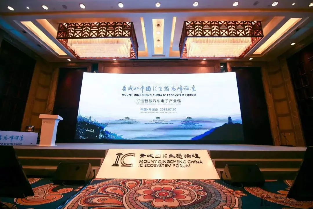
FD-SOI was a very important topic during the recent Mount Qingcheng China IC Ecosystem Forum. To situate things, Mount Qingcheng, with its lush hills and waterways, is located just outside of Chengdu. That of course is where GlobalFoundries is building its new fab, which will be the first in China to run FD-SOI. Chengdu is also a key city in China's automotive electronics landscape. [caption id="attachment_12236" align="alignright" width="300"] (Image Courtesy: VeriSilicon)[/caption] The theme of the forum was Building a Smart Automotive Electronics Industry Chain. Over 260 decision-makers from government, academia and industry attended – and the SOI Consortium had a significant presence. The event was chaired by Wayne Dai, CEO/Founder of consortium member VeriSilicon, and tireless champion of the the FD-SOI ecosystem in China and worldwide. Morning keynotes were given by: Carlos Mazure, Soitec CTO and SOI Consortium Executive Co-Director; Mark Granger, GF's VP of Automotive Product Line Management; and Tony King-Smith, Executive Advisor at AImotive, a GF 22FDX customer. BTW, transcripts of all the talks are available through Gasgoo, China's largest automotive B2B marketplace. You can click here to access them. (They're in Chinese – but you can open them in the language of your choice using the major translation websites.) Chengdu Officials Affirm Support for FD-SOI Fan Yi, Deputy Mayor of Chengdu, spoke extensively of FD-SOI in his keynote on the importance of rapidly developing smart cars. He heralded the “spectacular” new GlobalFoundries fab there. Following a meeting with the company's top brass the day before, he affirmed GF's confidence in their investment. There is a solid roadmap for FD-SOI, he noted, and efforts are underway to accelerate the move into production and expand education and training. He cited the benefits of FD-SOI for the entire supply chain, from design through package and test, raising the level of the entire IC industry to new heights. The government, he said, attaches great importance to this enterprise. Their thinking regarding intelligent transport in China is integrated with the overall approach to smart cities. SOI Consortium Leads Industry Keynotes [caption id="attachment_12232" align="alignleft" width="300"] Wayne Dai, VeriSilicon Founder and CEO (Photo courtesy VeriSilicon)[/caption] In his opening remarks, Wayne Dai emphasized the need for China to seize the advantage in the next round of development opportunities in the automotive electronics industry. This year's Qingcheng forum, he noted, brought together key representatives from across the supply chain, from of the highest to the deepest reaches of the smart car electronics industry, and across markets, technologies, solutions, industrial ecosystem, standards and regulations. In his talk on how FD-SOI is boosting the accelerated development of automotive electronics, Carlos Mazure presented the SOI Industry Consortium. He noted that the Consortium promotes mutual understanding and development across the ecosystem. SOI is already present throughout automotive applications, he noted. There are currently about 100mm2 of SOI per car, in such diverse areas power systems, transmissions, entertainment, in-vehicle networking and more. SOI will experience especially high growth in electrification, information/entertainment, networking, 5G, AI/edge computing and ADAS. He then went on to give some history and an extensive overview of the major trends and highlights we've seen over recent years. He finished by giving examples of convergence across the supply chain with IC manufacturers working with automakers to lower power, increase processor performance and advance 5G. [caption id="attachment_12233" align="alignright" width="665"] Carlos Mazure, Soitec CTO and SOI Consortium Executive Co-Director; Tony King-Smith, Executive Advisor at AImotive and Mark Granger, GF's VP of Automotive Product Line Management (Photo courtesy VeriSilicon)[/caption] GF's Mark Granger addressed the rapid development of automotive electronics. In certain areas, he said, he sees growth rates of over 20%. They are working on building the Chengdu ecosystem, especially for design, and in cooperation with the rest of the supply chain. Furthermore, he reminded the audience, when you talk about cars, travel implies that you also talk about IoT as well as things like infotainment and integrated radar ICs. In addition to cost and power efficiencies, the AEC-Q100 standard for IC reliability in automotive applications is also pushing designers to turn to FD-SOI. In the GF meeting with Chengdu government officials (referenced above in deputy mayor Fan Yi's talk), he too confirmed their support of FD-SOI as a key technology for China. GF is currently cooperating with about 75 automotive partners, he said, and the company is looking to increase cooperation with partners in the Chengdu region. Tony King-Smith talked about the 22FDX test chip AImotive is doing with Verisilicon and GF. In case you missed it, in June 2017 AImotive announced its AI-optimized hardware IP was available to global chip manufacturers for license. AiWare is built from the ground up for running neural networks, and the company says it is up to 20 times more power efficient than other leading AI acceleration hardware solutions on the market. In the same announcement, they revealed that VeriSilicon would be the first to integrate aiWare into a chip design,and that aiWare-based test chips would be fabricated on GF's 22FDX. The chip is expected to debut this year. While the afternoon agenda was not specific to FD-SOI, it did focus on the "smart cockpit" and "intelligent driving", with talks by nine leading players in China's automotive IC and investment communities. ~ ~ ~Note: Many thanks to the folks at VeriSilicon, who wrote up this event for their WeChat feed, and shared photos with us here at ASN.
Read More
Some really innovative start-ups presented chips they're doing on FD-SOI at the SOI Consortium’s 2018 SOI Symposium in Silicon Valley. We'll cover those here in Part 3 of ASN's coverage, as well as a presentation on China by wafer-maker Simgui and the final panel discussion. BTW, if somehow you missed my coverage of the morning sessions about very cool new products and projects from NXP, Sony, Audi, Airbus and Andes Technology, be sure to click here to read it. And in the afternoon the foundry partners provided excellent insight into who's designing chips on FD-SOI, and VLSIresearch explained why. You can read that here. Some of the presentations are posted on the SOI Consortium Events page – but some won’t be. Either way, I’ll cover them here. Start-upsIneda Systems began as an ADAS start-up, and are now working on developing low-power SoCs for use in consumer and enterprise applications. They're using FD-SOI for their current family of chips. SVP Ramkumar Subramanian emphasized that NRE costs are really important for smaller designs. 22FDX, he said, enabled them to move from 40nm, and ramp to larger volumes. In February, GreenWaves Technologies, a fabless semiconductor startup designing disruptive ultra-low power embedded solutions for image, sound and vibration AI processing in sensing devices, announced its GAP8 IoT application processor. GAP8 evaluation boards can now be ordered. The GAP8 agile power management architecture combined with IOT low duty cycling is a perfect fit for FDSOI processes. CEO Loic Lietar talked about how it would be used in AI applications at the very edge, wherein only the necessary data should be uploaded to the cloud. Also in February, Dream Chips’ announced that its ADAS SoC fabbed in GlobalFoundries’ 22FDX (FD-SOI) technology was posting record power efficiency (you can read more about it in ASN's coverage at the time here.) Dream Chips is Germany’s largest independent Engineering Service Provider. At the symposium, CEO Jens Benndor's talked about their roadmap. [caption id="attachment_11865" align="alignleft" width="300"] (Courtesy: eVaderis, SOI Consortium)[/caption] eVaderis CEO Jean Pascal Bost talked about how data-intensive IoT applications are enabled with FD-SOI and embedded magnetoresistive non-volatile memory (eMRAM) technology. You can get the slides from his talk here. eVaderis has eflash-like and eSRAM-like eMRAM IP that covers most MCU applications. They also have an eMRAM compiler tool and high-value-added IP for 22FDX. They foresee impressive power savings at the system level with body biasing: 25x this year and up to 45x in 2020, so that intelligence can be brought to IoT. In February they announced that they are co-developing an ultra-low power MCU reference design using GF’s eMRAM technology on the 22FDX® platform. And in March eVaderis and Mentor/Siemens announced that eVaderis proprietary Magnetic Tunnel Junction (MTJ) model would be co-optimized with AFS to speed-up simulations and generations of embedded MRAM IPs and compiler products with good accuracy.An 22FDX MCU reference design project is underway, with tape-out in July '18. Reduced Energy Microsystems (REM) CEO William Coven talked about realizing near-threshold computing with 22FDX and low-power memories. REM has two products on 22FDX: their Neuron Vision SoC and 64-bit RISC-V IP cores. 22FDX, he says, has been fantastic. Simgui Jeffrey Wang, the CEO of wafer-maker Simgui looked at why China is promoting its IC industry. (In the SOI ecosystem, Simgui is particularly known for its RF-SOI wafers, which it produces using Soitec's Smart CutTM process.) This was more of an overview talk, not necessarily specific to the SOI ecosystem, but certainly interesting. In terms of worldwide semiconductor sales, he said, about half end up in China. The CICF – aka the Big Fund – is currently running at about $74 billion. Having realized that mergers acquisitions would not solve the problem, they've opened a second round, targeting another $160 billion. China's two biggest innovation success stories are Huawei (with its Kirin processor), and China Rail, which is now a global Fortune 500 company. The CAGR for the China semiconductor industry is 19%, though they need 20% to reach their goals. IC design is a particularly successful area, posting a CAGR of 29%, with two players in China in the top 10 worldwide. Packaging and assembly/test are also very strong. Zing is working on increasing the supply of 300mm silicon wafers, while Simgui is expanding in both 200 and 300mm capex, due to “big demand”, he said. Panel Discussion [caption id="attachment_11866" align="alignleft" width="300"] SOI Symposium Panel Discussion: (left to right): Giorgio Cesana (Co-Director SOI Consortium), Dave Eggleston (VP GF), Tim Saxe (CTO, Quicklogic), Wayne Dai (CEO, Verisilicon), Samir Patel, (CEO Sankalp Semi), Kelvin Low (VP, ARM), Mahesh Tirupattur (EVP, Analog Bits)[/caption] The day wrapped up with an excellent panel discussion moderated by SOI Consortium Executive Co-Director Giorgio Cesana. Here are a few of the observations made by the panelists. QuickLogic CTO Tim Saxe said that FD-SOI made their designs more compact. With FD-SOI for FPGAs, you've got one set of IP, and you can decide at runtime where you're going for low power or high performance. With a lot of power domains, you see the benefits at the system level. GF VP Dave Eggleston said they're seeing early adopters of eMRAM, especially for wearables with RF and low power. ARM VP Kelvin Low said people should do more than just migrate to FD-SOI. If they use back biasing, it can replace the need for big/little cores. Body biasing makes things easier, maintained Verisilicon CEO Wayne Dai. His teams find that with body biasing, you can tape out for “typical” instead of “worst case”. It's not too late for FD-SOI: it's perfect timing for the MCU market, which is still at 40nm, said Sankalp Semi CEO Samir Patel. As designers, they're happy to focus on companies still on the older nodes. The IP ecosystem should be more enthusiastic about FD-SOI, said Analog Bits EVP Mahesh Tirupattur. You've got more potential customers, and your volume runs can be bigger. In his closing remarks, SOI Consortium Executive Co-Director Carlos Mazure reminded the audience of the day's three take-aways: power consumption is driving even systems companies FD-SOI is penetrating fields like MCUs and SoCs where more intelligence is needed China is still a really big opportunity.
Read More
EDA companies Cadence, Synopsys and Silvaco all gave excellent presentations at the SOI Consortium forums in Nanjing and Shanghai.Here's a recap of what the Cadence folks said. (I'll cover the Synopsys and Silvaco presentations in my next posts.)Design WinsAt the Shanghai FD-SOI Forum. Dr. Qui Wang, VP Chief of Staff, talked about FD-SOI Foundry Enablement: From Concept to Mass Production. Cadence, he reminded the packed ballroom, is not just EDA, but also system design enablement targeting verticals. “We’re ready!” he stated.In the last three years, they’ve done a lot of work on FD-SOI, he said, even working with ARM, GF and Dream Chip on the demo board as a reference design for automotive or vision applications, to show real data to their customers. It uses a quad implementation of the configurable Tensilica Vision P6 core.To simplify back biasing for the library folks, they worked with the foundries to create interpolations. And as Cadence is traditionally strong in RF/mixed-signal, there’s a new back-biasing tool to simplify board-chip communications, and make the bridge between power and thermal analysis.Cadence Has It All Jonathon Smith, Director of Strategic Alliances at Cadence, presented Enabling an Interconnected Digital World -- Cadence EDA IP Update at the Nanjing SOI summit. As he explained, his job is to ensure that design customers can use Cadence tools effectively, not just with Cadence IP, but also with 3rd party IP for the foundry nodes.He pointed out that the numbers for IoT predictions vary widely, and that industrial IoT (IIoT) will probably account for about 10% of the market. What is sure is that it will contain a large mixed-signal component (RF/digital/analog) and complex packaging.His customers want to know how fast and easy it is to work in FD-SOI. “Cadence custom and digital tools are ready for FD-SOI,” he said. They have the PDKs and tech files, and the EDA tools are enabled. The reference flows (both digital and custom analog) are tested and ready (Cadence customers who use p-cells and RF look especially for a good mixed-signal flow). [caption id="attachment_11432" align="alignnone" width="768"] EDA requirements for FD-SOI are complete. (Courtesy: Cadence SOI Consortium)[/caption] Customers also ask for proof points, and want to know the number of tape-outs they’ve done, performance benchmarks for working silicon and proven IP: this is what gives designers confidence, he said. Examples like Dream Chip’s Computer Vision Processor Chip Design for automotive ADAS CNN applications in 22nm FD-SOI (which they announced at Mobile World Congress in 2017 – see the press release here) have really helped build confidence further, he observed. (In case you missed it, DreamChip presented at the Silicon Valley SOI event in April 2017 – you can get that presentation here.)Cadence sees SOI as a driving force in IoT markets. They’ve also had some big digital wins recently, he added, and have made some major announcements with the foundries.For example, in September, they announced that their set of Design for Manufacturing (DFM) tools (signoff solutions) are now qualified on Samsung’s 28nm FD-SOI. This enables customers to create complex, advanced-node designs for the automotive, mobile, IoT, high-performance compute (HPC) and consumer markets (read the press release here). The Samsung Foundry's PDKs for 28nm FD-SOI are available for download now and incorporate the Cadence Litho Physical Analyzer (LPA), Physical Verification System (PVS) and Cadence CMP Predictor (CCP). In addition to signoff quality, the Cadence DFM tools offer an integration with the Virtuoso® platform and the Innovus™ Implementation System, providing designers with automated fixing capabilities and overall ease of use.And in October, Cadence announced that its digital and signoff flow, from synthesis to timing and power analysis, supports body-bias interpolation for GlobalFoundries 22FDX™ (read the press release here). The Cadence® tools enable advanced-node customers across a variety of vertical markets—including automotive, mobile, IoT and consumer applications—to use GF’s FD-SOI architecture to optimize power, performance and area (PPA).Cadence tools for ST’s 28nm FD-SOI foundry process were ready in 2016, btw – there’s a nice video testimonial from ST on power signoff, for example, which you can see here.
Read More
They're calling it, “The most advanced, lowest power-consuming GPU-enabled MPU on the market.” It's NXP's new i.MX 7ULP general-purpose processor, and it's on 28nm FD-SOI. They've got a nifty video summing it all up – you can watch it here. [caption id="attachment_10388" align="alignleft" width="300"] NXP is first to market with a general-purpose processor on FD-SOI: the i.MX 7ULP. It's got both ultra-low power consumption and rich graphics for battery powered applications. (Courtesy: NXP)[/caption] With the i.MX 7ULP, NXP is first to market with an FD-SOI applications processor offering the industry’s lowest power consumption. The debut was made at the recent Embedded World Conference in Nuremberg, Germany, and it made a big splash in media across the globe. (Read the full press release here.) In deep sleep mode, it boasts power consumption of just 15 uW or less: 17 times less than previous (and highly successful) low power i.MX 7 devices. Dynamic power efficiency is improved by 50 percent on the real-time domain.The i.MX 7ULP applications processor family is currently sampling to select customers. Broader availability of pre-production samples is scheduled for Q3 2017.Hello, IoT!The high-performance, low-power solution is optimized for customers developing applications that spend a significant amount of time in standby mode with short bursts of performance-intense activity that require exceptional graphics processing. Sounds like IoT – and indeed it is, and more.With the i.MX 7ULP, NXP's targeting wearables, portable healthcare, smart home controls, gaming accessories, building automation, general embedded control and IoT edge solutions. Bottom line: it's designed to enable ultra-low-power and secure, portable applications – especially those demanding long battery life. (Read the current fact sheet here.)The detailsThe i.MX 7ULP features an advanced implementation of the ARM® Cortex®-A7 core, the ARM Cortex-M4 core, as well as a 3D and 2D Graphic Processing Units (GPUs). It's got a 32-bit LPDDR2/LPDDR3 memory interface and a number of other interfaces for connecting peripherals, such as WLAN, Bluetooth, GPS, displays, and camera sensors. [caption id="attachment_10387" align="alignnone" width="834"] (Courtesy: NXP)[/caption] NXP says this new design, based on FD-SOI’s lower voltage capability, enables rich user experience through extremely power-efficient graphics acceleration, a fundamental requirement in many of today’s consumer and industrial battery-operated devices that incorporate robust graphic interfaces. Further enablement includes rich Linux or Android ecosystem with the real-time capability supported by FreeRTOS.Leveraging body biasing and moreNXP credits the design’s extreme low leakage and operating voltage (Vdd) scalability to that FD-SOI specialty: reverse and forward body biasing (RBB/FBB) of the transistors, and its smart power system architecture.In presenting the new i.MX 7ULP to the tech press, the company highlighted the following FD-SOI design advantages: Large dynamic gate and body biasing voltage range Domain and subsystem optimization with custom standard cell library with mixed voltages Low quiescent current (Iq) bias generators Enhanced ADC performance with unique FD-SOI attributes Fail Safe I/O for simplified low power system design To that, add a note about security. As the chip's fact sheet says, “The processors deliver hardware-enabled security features that enable secure e-commerce, digital rights management (DRM), information encryption secure boot, and tamper detection.” Those are just the sort of things that demand the bursts of high performance that dynamic forward body biasing delivers where and when it's needed.Samsung fabs, Verisilicon adds IPTwo other SOI Consortium members – Samsung and Verisilicon – are particularly pleased with NXP's results.“We are excited that NXP is the first to bring the benefits of FD-SOI (28FDS) technology to the general purpose market,” says Ryan Lee, VP of the Foundry Marketing Team at Samsung Electronics. “28FDS technology will satisfy a growing and critical need for ultra low power designs that require power-performance at very low voltages. We plan to evolve 28FDS technology to a differentiated low-power single platform by implementing RF and embedded Non-Volatile Memory (eNVM) solution for our customers’ success.”NXP’s processor design enables robust low power graphics for the IoT and wearable markets through two graphic processor units (GPU) from Vivante: the GC7000 NanoUltra 3D GPU with a low power single shader, and the GC320 Composition Processing Core (CPC) for 2D graphics. The 3D GPU plays a critical role in enabling rich 3D based user interfaces, while the CPC can accelerate both rich 3D and simpler 2D user interfaces. Processors based on the combination of the two GPUs enable efficient display systems which offload and significantly reduce system resources, in turn providing rich user interfaces at low power levels to extend the battery life of devices.“Our 3D GPU is a result of a joint collaboration between Vivante and NXP to deliver industry-leading 3D capabilities with the lowest power consumption,” said Wei-Jin Dai CEO at Vivante Corporation and Chief Strategy Officer and GM of the IP Division at Verisilicon. “The power savings from using the right GPU in an ultra low power processor is one of the major attributes and advantages of the architecture.”So, now shall we dig in a little deeper into the “why FD-SOI” question? Read on in Part 2 of this article.-- By Adele Hars, ASN Editor-in-Chief
Read More
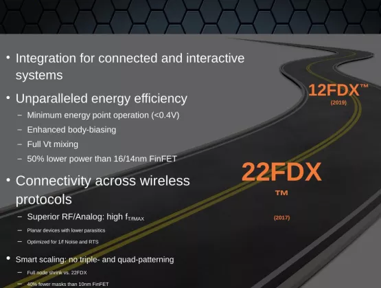
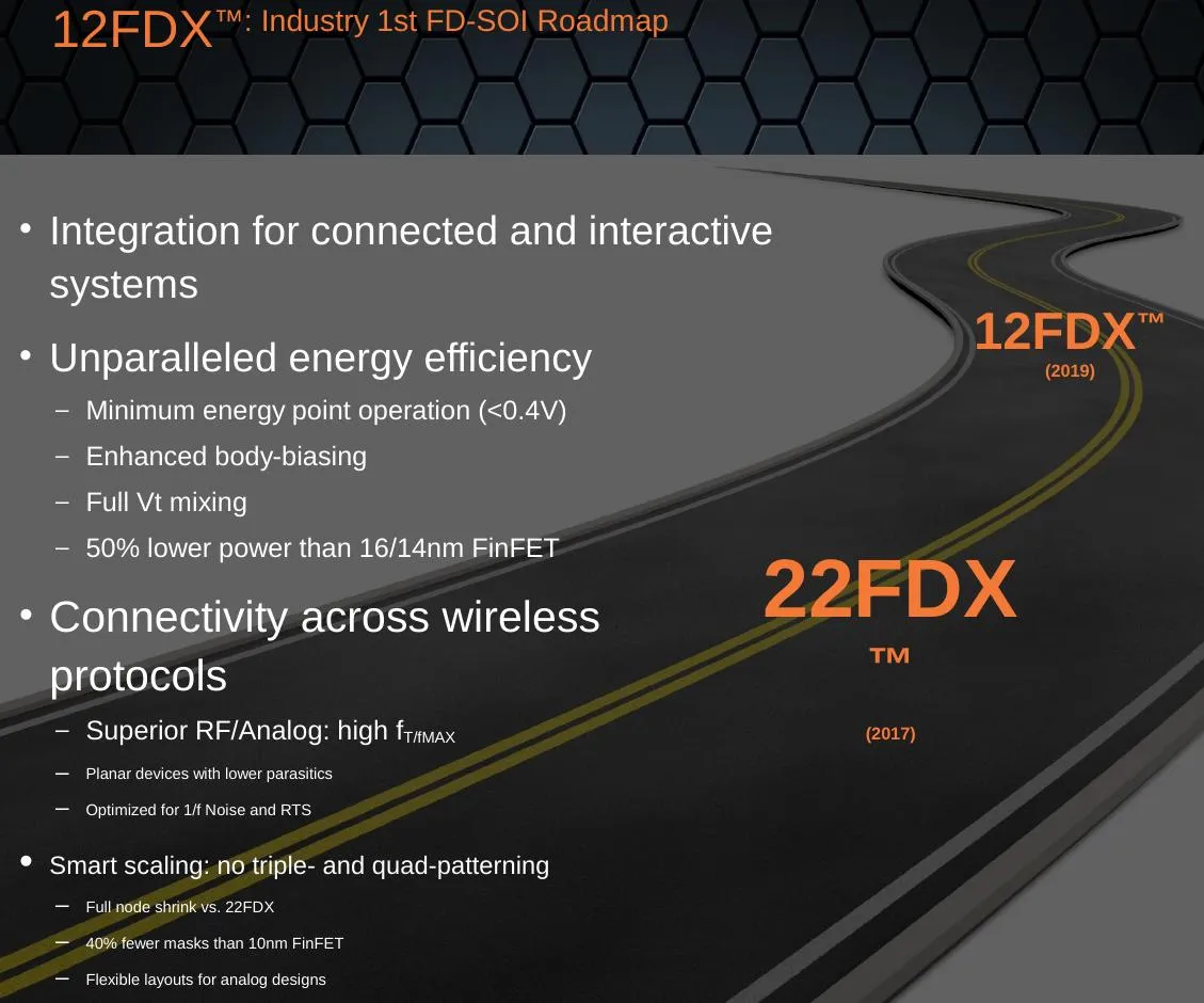
12nm FD-SOI has now officially joined the GlobalFoundries’ roadmap, targeting intelligent, connected systems and beating 14/16nm FinFET on performance, power consumption (by 50%!) and cost (see press release here). Customer product tape-outs are expected to begin in the first half of 2019. GloFo also announced FDXcelerator™, an ecosystem designed to give 22FDX™ SoC design a boost and reduce time-to-market for its customers (press release here). [caption id="attachment_9874" align="aligncenter" width="610"] (Courtesy: GlobalFoundries and SOI Consortium Shanghai FD-SOI Forum 2016)[/caption] The news turned heads worldwide (hundreds of publications immediately picked up the news) – and especially in China. "We are excited about the GlobalFoundries 12FDX offering and the value it can provide to customers in China," said Dr. Xi Wang, Director General, Academician of Chinese Academy of Sciences, Shanghai Institute of Microsystem and Information Technology. “Extending the FD-SOI roadmap will enable customers in markets such as mobile, IoT, and automotive to leverage the power efficiency and performance benefits of the FDX technologies to create competitive products." Wayne Dai, CEO of VeriSilicon (headquartered in Shanghai but designing for the world’s biggest names in the chip biz), added, “We look forward to extending our collaboration with GlobalFoundries on their 12FDX offering and providing high-quality, low-power and cost-effective solutions to our customers for the China market. The unique benefits of FD-SOI technologies enable us to differentiate in the automotive, IoT, mobility, and consumer market segments.” The ultra-thin FD-SOI wafers are where it all starts, and they’re ready to go in high volume, says Paul Boudre, CEO of SOI wafer leader Soitec. “We are very pleased to see a strong momentum and a very solid adoption from fabless customers in 22FDX offering,” he adds. “Now this new 12FDX offering will further expand FD-SOI market adoption. This is an amazing opportunity for our industry just in time to support a big wave of new mobile and connected applications.” All About 12GloFo’s 12FDXTM platform, which builds on the success of its 22FDXTM offering, is designed to enable the intelligent systems of tomorrow across a range of applications, from mobile computing and 5G connectivity to artificial intelligence and autonomous vehicles. Increased integration of intelligent components including wireless (RF) connectivity, non-volatile memory, and power management—all while driving ultra-low power consumption—are key 12FDX selling points that FinFETs can’t touch. The technology also provides the industry’s widest range of dynamic voltage scaling and unmatched design flexibility via software-controlled transistors—capable of delivering peak performance when and where it is needed, while balancing static and dynamic power for the ultimate in energy efficiency. [caption id="attachment_9873" align="aligncenter" width="610"] (Courtesy: GlobalFoundries and SOI Consortium Shanghai FD-SOI Forum 2016)[/caption] “Some applications require the unsurpassed performance of FinFET transistors, but the vast majority of connected devices need high levels of integration and more flexibility for performance and power consumption, at costs FinFET cannot achieve,” said GLOBALFOUNDRIES CEO Sanjay Jha. “Our 22FDX and 12FDX technologies fill a gap in the industry’s roadmap by providing an alternative path for the next generation of connected intelligent systems. And with our FDX platforms, the cost of design is significantly lower, reopening the door for advanced node migration and spurring increased innovation across the ecosystem.” Kudos came in from G. Dan Hutcheson, CEO of VLSI Research, IBS CEO Handel Jones, Linley Group Founder Linley Gwennap, Dasaradha Gude, CEO of IP/design specialists INVECAS, Leti CEO Marie Semeria and NXP VP Ron Martino (they’ve already started on 28nm FD-SOI for their i.MX line – read his superb explanations in ASN here). 22 Design Plug ‘n PlaySimultaneously to the 12FDX announcement, GloFo announced the FDXcelerator Partner Program. It creates an open framework under which selected Partners can integrate their products or services into a validated, plug and play catalog of design solutions. This level of integration allows customers to create high performance designs while minimizing development costs through access to a broad set of quality offerings, specific to 22FDX technology. The Partner ecosystem positions members and customers to take advantage of the broad adoption and accelerating growth of the FDX market.Initial partners of the FDXcelerator Partner Program are: Synopsys (EDA), Cadence (EDA), INVECAS (IP and Design Solutions), VeriSilicon (ASIC), CEA Leti (services), Dreamchip (reference solutions) and Encore Semi (services). These companies have already initiated work to deliver advanced 22FDX SoC solutions and services. Initial FDXcelerator Partners have committed a set of key offerings to the program, including: tools (EDA) that complement industry leading design flows by adding specific modules to easily leverage FDSOI body-bias differentiated features, a comprehensive library of design elements (IP), including foundation IP, interfaces and complex IP to enable foundry customers to start their designs from validated IP elements, platforms (ASIC), which allow a customer to build a complete ASIC offering on 22FDX, reference solutions (reference designs, system IP), whereby the Partner brings system level expertise in Emerging application areas, enabling customers to speed-up time to market, resources (design consultation, services), whereby Partners have trained dedicated resources to support 22FDX technology; and product packaging and test (OSAT) solutions. Additional FDXcelerator members will be announced in the following months.
Read More