downloadGroupGroupnoun_press release_995423_000000 copyGroupnoun_Feed_96767_000000Group 19noun_pictures_1817522_000000Member company iconResource item iconStore item iconGroup 19Group 19noun_Photo_2085192_000000 Copynoun_presentation_2096081_000000Group 19Group Copy 7noun_webinar_692730_000000Path
Skip to main content
Default Banner Image

Cadence

FD-SOI for RF and mmWave communications is a hot topic. In high-data rate communications like RF and millimeter-wave devices in particular, FD-SOI delivers high-performance with numerous unique advantages, making it most likely the fastest RF-CMOS technology on the market. If you’d like to take a deep dive and learn more about it, Soitec and Incize are sponsoring a free, full-day workshop in Grenoble on April 4th, 2019. Click here for registration information. The workshop follows the day after the IEEE/EDS EuroSOI-ULIS conference there (you can read about the full conference in a previous ASN post). This technical workshop will cover the FD-SOI technology platform with a focus on its compatibility with RF mmWave communications. Attendees will hear from notable FD-SOI leaders and experts from leading industry and research institutions presenting updates on key developments and building blocks across the semiconductor value chain. Topics will include circuit design, device fundamentals, simulation and characterization of RF devices, test, CMOS technology and substrate technologies enabling FD-SOI. In addition, the workshop will include an overview about how FD-SOI technology is benefiting current and future end user applications. Here’s the agenda: [caption id="attachment_15990" align="alignleft" width="945"] FD-SOI technology platform: new standards for emerging consumer electronics [Click to enlarge.][/caption]
Read More
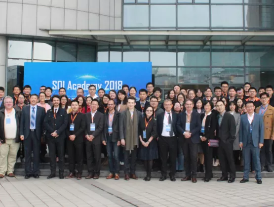
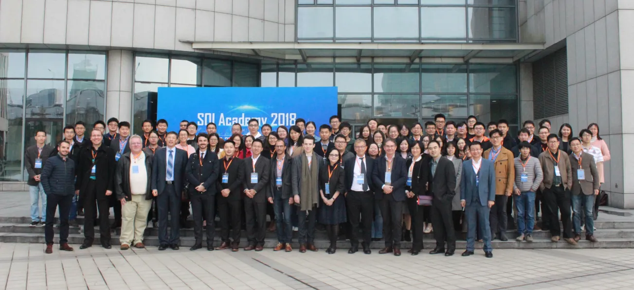
There were over 220 participants at the recent SOI Academy FD-SOI Training event organized in Shanghai. The event extended over two days, with the first day covering a basic introduction to the technology as well as the ecosystem worldwide and in China. The second day was hands-on professional training. Attendees got a comprehensive understanding of how to leverage the benefits and flexibility of FD-SOI design techniques for low-power chips including logic, mixed-signal/RF and analog blocks. They had a great line-up of experts from whom to learn – check out the agenda here. There was also a follow-up press release (in Chinese) from SITRI here. There will be more of these SOI Academy events in cities across China in the year to come – we'll keep you posted (and of course, keep checking back for news on the Consortium's Events page). [caption id="attachment_12981" align="aligncenter" width="1000"] SOI Academy '18 keynotes by: Dr. Mark Ding, CEO, SITRI; Dr. Carlos Mazure, EVP Soitec and Chairman/Executive Director SOI Consortium. Dr. Julien Arcamone, EVP Leti. (Images courtesy: SITRI). Lower right: the hands-on FD-SOI training.[/caption] The two-day seminar and hands-on FD-SOI design training was (superbly!) co-organized by SITRI and Leti, with the support of the SOI Industry Consortium at the Jiading SIMIT campus outside of Shanghai. Just to put this in perspective, SIMIT and SITRI are absolutely key players in China's chip ecosystem. SIMIT is the Shanghai Institute of Microsystem and Information Technology, one of the most venerable institutes in the Chinese Academy of Science (CAS) and one of the world's earliest pioneers in SOI. SITRI is the Shanghai Industrial μTechnology Research Institute, an international innovation center focused on globally accelerating innovation and commercialization of More-than-Moore for IoT. Both institutions are under the aegis of Dr. Xi Wang, Chairman of SITRI, Director General of SIMIT, Academician of CAS, and champion of all things SOI in China. At this Shanghai event, the participants came from industry (including big companies, SMEs and startups) and technical institutions. In fact as well as attendees from Shanghai people voyaged from other cities such as Shenzhen and Chengdu. The designers participating to the FD-SOI training day were all experienced in design and highly motivated in learning FD-SOI design, notes Carlos Mazure, Chairman Executive Director of the SOI Industry Consortium, and Executive VP of Soitec. “This made it possible to dive into the specificities of FD-SOI,” he said, adding that, “The focus on RF was very timely.” Day 1: Intro to FD-SOI The first afternoon opening keynotes were made by SITRI CEO Dr. Mark Ding and Leti EVP Dr. Julien Arcamone. These were followed by overview talks by execs from Soitec, Verisilicon and GlobalFoundries. After a lively networking break, three talks delved into FD-SOI technology. The first was by Professor Sorin Cristoloveanu, Laureate of the IEEE Andrew Grove Award and Director at the CNRS (the French National Center for Scientific Research – the largest governmental research organization in France and the largest fundamental science agency in Europe). He covered device physics and characterization techniques. This was followed by talks on the technology by Soitec Fellow Bich-Yen Nguygen, and by Dr. Christophe Tretz, IBM Sr. Engineer on product design methodology. The day ended with a dinner, where Professor Cristoloveanu says enthusiastic technical discussions continued unabated (and continued even further in follow-up emails), lots of business cards were exchanged, and opportunities for further education were explored. Day 2: Hands-on Training The second day, designers got hands-on training from Leti experts using FD-SOI PDKs, first in the morning on digital, then in the afternoon on RF. Everyone loved the lively discussion and in-depth exchanges between the experts and the designers. They agreed that FD-SOI has important applications and differentiated competitive advantages for IoT, 5G, automotive, AI and other fields. At the end of the training, Leti and SITRI jointly issued SOI Academy certificates of completion to the designers. Feedback from participants was very good. Some asked for further education and for hands-on testimonials from companies that are already designing and manufacturing products on FD-SOI. “The participants were focused, motivated, involved, with good knowledge, which helped make the three hours of Digital training effective,” said Dr. Alexandre Valentian, Leti Sr. Expert, Digital Design. “The IT team was very helpful in setting up the training, the students accounts and the hardware infrastructure.” “The training on Basics of FD-SOI RF circuit was a great success thanks to the efficiency of our Chinese partners and also thanks to the enthusiasm and the good level of our trainees. As senior Expert of CEA Leti I was really impressed by the professionalism of the organization team. For all these reasons, I’m very glad to have had the opportunity to contribute to the 2018 SOI Academy,” said Dr. Baudouin Martineau, Leti Sr. Expert, RFIC Design Technologies. “The professionalism, efficiency and enthusiasm of our Chinese partners and the level and technical relevance of all trainees made the training on Basics of FD-SOI RF circuit a great success and fruitful experience,” added Frédéric Hameau, Sr. RF Research Engineer, Leti Project Leader, Architecture, IC Design Embedded Software Division, RF Architectures and ICs Laboratory. “It was a pleasure to get the opportunity to be part of this first edition of SOI academy 2018.” The organizers would like to thank the sponsors, including: the SOI Consortium and its members Soitec, VeriSilicon, GlobalFoundries, Simgui and Cadence, as well as Mentor, ProPlus and other companies and institutions in China and worldwide. Dr. Mazure notes that special recognition must go to Dr. Julien Arcamone, EVP, Leti-CEA and to Qing Wang-Bousquet, SITRI representative, for the perfect and smooth organization, and to the Leti instructors, who are international experts and highly committed. “As one of the main initiators and organizers of the 2018 SOI Academy, I wanted to personally thank all of you for your respective contribution to this first edition of the SOI Academy,” concludes Dr. Arcamone. “Undoubtedly, it was a great success, very well organized and fluid and we can be proud of that.”
Read More
Intento Design is working with STMicroelectronics to bring ID-XploreTM EDA software, which is aimed at solving the critical analog design challenges, to FD-SOI process nodes. “ID-Xplore is a disruptive EDA software that accelerates analog design and migration processes by at least one order of magnitude. It reduces the cost and latency inherent to analog design. Currently, there is no similar EDA tool on the market covering the analog design challenges like ID-Xplore,” noted Dr. Ramy Iskander, CEO of Intento Design (see the press release here). ST's FD-SOI design expertise roots, of course, are as deep as they get. “ST’s decision to work with us confirms the relevance of our solution. We are very excited to work jointly with ST teams to take the most benefit out of FD-SOI technology leveraging ST’s pioneering leadership in this area,” continued Dr. Iskander. “We’ve already seen the benefits of ID-Xplore in accelerating the design phase of different analog circuits, thanks to the software’s fast and accurate exploration capabilities in advanced FD-SOI processes,” said Thierry Bion, ST's Hardware Design Director, Aerospace Defense Legacy Division. “By facilitating IP reuse and sharing of design insights between engineers, ID-Xplore™ is helping our teams significantly accelerate new product introductions.” ID-Xplore uses the OpenAccess database standard and is fully integrated within the Cadence design environment. The designer’s implicit and explicit knowledge is expressed as technology-independent constraints, bringing the designers back to their core expertise and creativity. If you want to learn more, the folks over at semiwiki.com have made a number of posts on Intento Design recently. They're really helpful in understanding what the company does, how and why: CEO Interview: Ramy Iskander of Intento Design Edit (by Daniel Nenni) – good backgrounder on the company and product. The Intention View: Disruptive Innovation for Analog Design Edit (by Daniel Nenni) – an excellent interview with Dr. Caitlin Brandon about how the tool works and how it aligns with and supports the way analog designers work. A New Kind of Analog EDA Company Edit (by Daniel Payne) – Daniel Payne started his career as a circuit designer at Intel, and is now a well-known consultant/expert in the EDA world. Here he explores how ID-Xplore actually works and its “cool new automation features”.
Read More
GlobalFoundries' new ecosystem partner program, called RFwave™, aims to simplify RF design and help customers reduce time-to-market for a new era of wireless devices and networks (read the full press release here). The program aims to give designers a low-risk, cost-effective path to highly optimized solutions that leverage GF's platforms including RF on FD-SOI and RF-SOI. The target is wireless applications such as IoT across various wireless connectivity and cellular standards, standalone or transceiver integrated 5G front end modules, mmWave backhaul, automotive radar, small cell and fixed wireless and satellite broadband. As such, the RFwave™ partner program provides GF customers with IP design elements, EDA tools, design consultation and services and OSAT product packaging and test solutions. These products and services are validated, and comprise a plug-and-play catalog of design solutions. With this level of integration, GF customers can create high-performance designs while minimizing development costs. Bami Bastani, senior vice president of GF’S RF Business Unit, says, “As a leader in RF, GF’s RFwave program takes industry collaboration to a new level, enabling our customers to build differentiated, highly integrated RF-tailored solutions that are designed to accelerate the next wave of technology.” Initial members of the RFwave Partner Program are: asicNorth, Cadence, CoreHW, CWS, Keysight Technologies, Spectral Design, and WEASIC.
Read More
RF-SOI is in every smart phone out there, and with 5G, there are lots more applications on the horizon. If you’d like to learn more about designing in RF-SOI, there’s a great short course coming up the day before and in conjunction with the EuroSOI-ULIS Conference in Granada, Spain.The title of this short course is RFSOI: from basics to practical use of wireless technology. Program and registration details can be found here. The course runs for the full day on Sunday, 18 March 2018.The talks, which are being given by a stellar line-up of experts, include: RF SOI, fabrication, materials and eco-system - Ionut Radu Director of Advanced R D, Soitec Fundamentals of RF SOI technology - Jean-Pierre Raskin, Professor, UCL 22nm FDSOI Technology optimized for RF/mmWave Applications - David L. Harame, RF CTO Development and Enablement, GlobalFoundries RF SOI technology and components for 5G connectivity - Christine Raynaud, Program Manager (Business Development – Technology to Design), CEA-Leti Analog and RF design on SOI - Barend van Liempd, Senior Researcher, imec Techniques and tricks for RF measurements on SOI - Andrej Rumiantsev, Director RF Technologies, MPI Corporation FOSS TCAD/EDA tools for advanced SOI-device modeling - Wladek Grabinski, R D CM Manager, MOS-AK RF design flow for SOI - Ian Dennison, Design Systems Senior Group Director, Cadence The course is being organized by SOI Consortium members Incize and Soitec. BTW, this year marks the 4th joint EUROSOI – ULIS Conference. The EuroSOI Conference, which has been ongoing for decades, is well paired with the ULtimate Integration on Silicon Conference. The joint conference provides an interactive forum for scientists and engineers working in the field of SOI technology and advanced nanoscale devices. One of the key objectives is to promote collaboration and partnership between different players from academia, research and industry. As such, it covers technical topics, industry trends and updates from pertinent European programs. EuroSOI-ULIS will take place 19–21 March 2018 at the University of Granada in Spain. For information on the program and how to register, see the website. Following the conference, the papers will be available at the IEEE Xplore® digital library, and the best papers will be published in a special issue of Solid-State Electronics.
Read More
EDA companies Cadence, Synopsys and Silvaco all gave excellent presentations at the SOI Consortium forums in Nanjing and Shanghai.Here's a recap of what the Cadence folks said. (I'll cover the Synopsys and Silvaco presentations in my next posts.)Design WinsAt the Shanghai FD-SOI Forum. Dr. Qui Wang, VP Chief of Staff, talked about FD-SOI Foundry Enablement: From Concept to Mass Production. Cadence, he reminded the packed ballroom, is not just EDA, but also system design enablement targeting verticals. “We’re ready!” he stated.In the last three years, they’ve done a lot of work on FD-SOI, he said, even working with ARM, GF and Dream Chip on the demo board as a reference design for automotive or vision applications, to show real data to their customers. It uses a quad implementation of the configurable Tensilica Vision P6 core.To simplify back biasing for the library folks, they worked with the foundries to create interpolations. And as Cadence is traditionally strong in RF/mixed-signal, there’s a new back-biasing tool to simplify board-chip communications, and make the bridge between power and thermal analysis.Cadence Has It All Jonathon Smith, Director of Strategic Alliances at Cadence, presented Enabling an Interconnected Digital World -- Cadence EDA IP Update at the Nanjing SOI summit. As he explained, his job is to ensure that design customers can use Cadence tools effectively, not just with Cadence IP, but also with 3rd party IP for the foundry nodes.He pointed out that the numbers for IoT predictions vary widely, and that industrial IoT (IIoT) will probably account for about 10% of the market. What is sure is that it will contain a large mixed-signal component (RF/digital/analog) and complex packaging.His customers want to know how fast and easy it is to work in FD-SOI. “Cadence custom and digital tools are ready for FD-SOI,” he said. They have the PDKs and tech files, and the EDA tools are enabled. The reference flows (both digital and custom analog) are tested and ready (Cadence customers who use p-cells and RF look especially for a good mixed-signal flow). [caption id="attachment_11432" align="alignnone" width="768"] EDA requirements for FD-SOI are complete. (Courtesy: Cadence SOI Consortium)[/caption] Customers also ask for proof points, and want to know the number of tape-outs they’ve done, performance benchmarks for working silicon and proven IP: this is what gives designers confidence, he said. Examples like Dream Chip’s Computer Vision Processor Chip Design for automotive ADAS CNN applications in 22nm FD-SOI (which they announced at Mobile World Congress in 2017 – see the press release here) have really helped build confidence further, he observed. (In case you missed it, DreamChip presented at the Silicon Valley SOI event in April 2017 – you can get that presentation here.)Cadence sees SOI as a driving force in IoT markets. They’ve also had some big digital wins recently, he added, and have made some major announcements with the foundries.For example, in September, they announced that their set of Design for Manufacturing (DFM) tools (signoff solutions) are now qualified on Samsung’s 28nm FD-SOI. This enables customers to create complex, advanced-node designs for the automotive, mobile, IoT, high-performance compute (HPC) and consumer markets (read the press release here). The Samsung Foundry's PDKs for 28nm FD-SOI are available for download now and incorporate the Cadence Litho Physical Analyzer (LPA), Physical Verification System (PVS) and Cadence CMP Predictor (CCP). In addition to signoff quality, the Cadence DFM tools offer an integration with the Virtuoso® platform and the Innovus™ Implementation System, providing designers with automated fixing capabilities and overall ease of use.And in October, Cadence announced that its digital and signoff flow, from synthesis to timing and power analysis, supports body-bias interpolation for GlobalFoundries 22FDX™ (read the press release here). The Cadence® tools enable advanced-node customers across a variety of vertical markets—including automotive, mobile, IoT and consumer applications—to use GF’s FD-SOI architecture to optimize power, performance and area (PPA).Cadence tools for ST’s 28nm FD-SOI foundry process were ready in 2016, btw – there’s a nice video testimonial from ST on power signoff, for example, which you can see here.
Read More
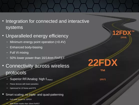
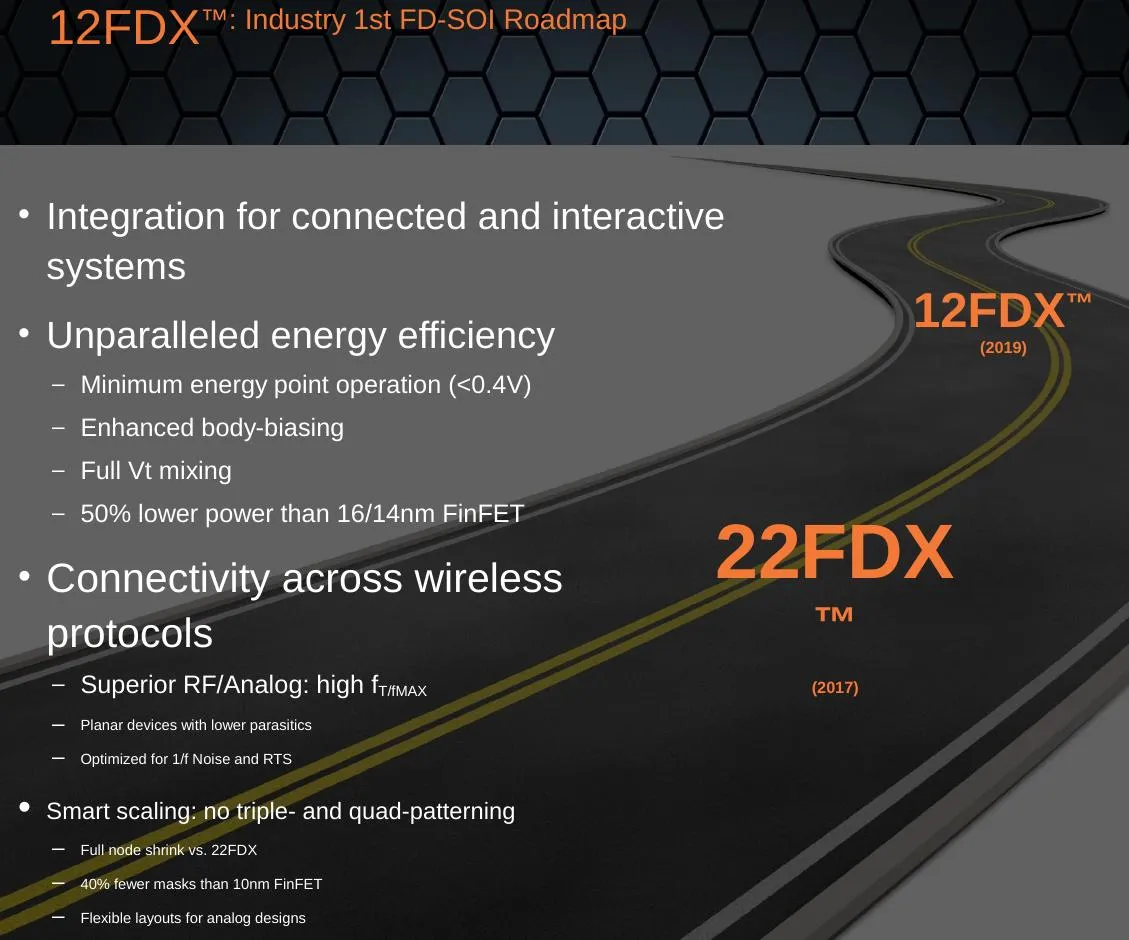
12nm FD-SOI has now officially joined the GlobalFoundries’ roadmap, targeting intelligent, connected systems and beating 14/16nm FinFET on performance, power consumption (by 50%!) and cost (see press release here). Customer product tape-outs are expected to begin in the first half of 2019. GloFo also announced FDXcelerator™, an ecosystem designed to give 22FDX™ SoC design a boost and reduce time-to-market for its customers (press release here). [caption id="attachment_9874" align="aligncenter" width="610"] (Courtesy: GlobalFoundries and SOI Consortium Shanghai FD-SOI Forum 2016)[/caption] The news turned heads worldwide (hundreds of publications immediately picked up the news) – and especially in China. "We are excited about the GlobalFoundries 12FDX offering and the value it can provide to customers in China," said Dr. Xi Wang, Director General, Academician of Chinese Academy of Sciences, Shanghai Institute of Microsystem and Information Technology. “Extending the FD-SOI roadmap will enable customers in markets such as mobile, IoT, and automotive to leverage the power efficiency and performance benefits of the FDX technologies to create competitive products." Wayne Dai, CEO of VeriSilicon (headquartered in Shanghai but designing for the world’s biggest names in the chip biz), added, “We look forward to extending our collaboration with GlobalFoundries on their 12FDX offering and providing high-quality, low-power and cost-effective solutions to our customers for the China market. The unique benefits of FD-SOI technologies enable us to differentiate in the automotive, IoT, mobility, and consumer market segments.” The ultra-thin FD-SOI wafers are where it all starts, and they’re ready to go in high volume, says Paul Boudre, CEO of SOI wafer leader Soitec. “We are very pleased to see a strong momentum and a very solid adoption from fabless customers in 22FDX offering,” he adds. “Now this new 12FDX offering will further expand FD-SOI market adoption. This is an amazing opportunity for our industry just in time to support a big wave of new mobile and connected applications.” All About 12GloFo’s 12FDXTM platform, which builds on the success of its 22FDXTM offering, is designed to enable the intelligent systems of tomorrow across a range of applications, from mobile computing and 5G connectivity to artificial intelligence and autonomous vehicles. Increased integration of intelligent components including wireless (RF) connectivity, non-volatile memory, and power management—all while driving ultra-low power consumption—are key 12FDX selling points that FinFETs can’t touch. The technology also provides the industry’s widest range of dynamic voltage scaling and unmatched design flexibility via software-controlled transistors—capable of delivering peak performance when and where it is needed, while balancing static and dynamic power for the ultimate in energy efficiency. [caption id="attachment_9873" align="aligncenter" width="610"] (Courtesy: GlobalFoundries and SOI Consortium Shanghai FD-SOI Forum 2016)[/caption] “Some applications require the unsurpassed performance of FinFET transistors, but the vast majority of connected devices need high levels of integration and more flexibility for performance and power consumption, at costs FinFET cannot achieve,” said GLOBALFOUNDRIES CEO Sanjay Jha. “Our 22FDX and 12FDX technologies fill a gap in the industry’s roadmap by providing an alternative path for the next generation of connected intelligent systems. And with our FDX platforms, the cost of design is significantly lower, reopening the door for advanced node migration and spurring increased innovation across the ecosystem.” Kudos came in from G. Dan Hutcheson, CEO of VLSI Research, IBS CEO Handel Jones, Linley Group Founder Linley Gwennap, Dasaradha Gude, CEO of IP/design specialists INVECAS, Leti CEO Marie Semeria and NXP VP Ron Martino (they’ve already started on 28nm FD-SOI for their i.MX line – read his superb explanations in ASN here). 22 Design Plug ‘n PlaySimultaneously to the 12FDX announcement, GloFo announced the FDXcelerator Partner Program. It creates an open framework under which selected Partners can integrate their products or services into a validated, plug and play catalog of design solutions. This level of integration allows customers to create high performance designs while minimizing development costs through access to a broad set of quality offerings, specific to 22FDX technology. The Partner ecosystem positions members and customers to take advantage of the broad adoption and accelerating growth of the FDX market.Initial partners of the FDXcelerator Partner Program are: Synopsys (EDA), Cadence (EDA), INVECAS (IP and Design Solutions), VeriSilicon (ASIC), CEA Leti (services), Dreamchip (reference solutions) and Encore Semi (services). These companies have already initiated work to deliver advanced 22FDX SoC solutions and services. Initial FDXcelerator Partners have committed a set of key offerings to the program, including: tools (EDA) that complement industry leading design flows by adding specific modules to easily leverage FDSOI body-bias differentiated features, a comprehensive library of design elements (IP), including foundation IP, interfaces and complex IP to enable foundry customers to start their designs from validated IP elements, platforms (ASIC), which allow a customer to build a complete ASIC offering on 22FDX, reference solutions (reference designs, system IP), whereby the Partner brings system level expertise in Emerging application areas, enabling customers to speed-up time to market, resources (design consultation, services), whereby Partners have trained dedicated resources to support 22FDX technology; and product packaging and test (OSAT) solutions. Additional FDXcelerator members will be announced in the following months.
Read More