“The ecosystem is ready. The focus is now on applications and products.” And with those words, SOI Consortium Executive Director Carlos Mazure opened the annual Silicon Valley SOI Symposium. As promised, the day was packed with presentations about products on FD-SOI – some from big players like NXP and Sony, some from names new to the FD-SOI ecosystem like Audi and Airbus, and some from start-ups just getting into the game.
The event got excellent coverage in EETimes/EDN – including in their editions across the globe in China, Japan, Taiwan, India and more. Samsung, GF Ramp FD-SOI, heralded the headlines.
It was a full day of excellent presentations. In this post, I'll chronicle the morning presentations. The next post(s) will cover the afternoon session. Note that as of this writing, the ppts are not yet posted on the SOI Consortium website, but many will be. Keep checking back under the Events tab, and look under “past Events”.
Andes Technology
As semiwiki noted a few years back, Andes Technology is “...the biggest microprocessor IP company you've never heard of.” Based in Taiwan, Mediatek is one of their big customers; they've got a strong client base across Asia/Pacific, and are now making inroads into North America. Last year they announced with GF their 32-bit CPU IP cores had been implemented on GF's 22FDX® FD-SOI technology.
In his symposium keynote, CEO Frankwell Lin said that in the test chip they're doing with GF and Invecus, they're seeing a 70% power savings compared with what they'd gotten in 28ULP. Their newest products are the N25 32bit and NX25 64bit RISC-V based cores, and in July they'll announce a core that runs on Linux.
NXP
“With FD-SOI we're enabling the future of embedded processing,” the always-quotable (and keynote speaker) NXP VP/GM Ron Martino told us. NXP's i.MX7ULP, i.MX8, i.MX8X and i.MXRT are all FD-SOI based. They all share fundamental building blocks, so NXP can build platforms, scale and re-use IP. “It's better than any technology I've worked on in my 30 years in the industry,” he said.
They're seeing much higher performance with on-chip flash. And the RT “crossover” processor boasts 3x higher computing performance than today's competing MCUs. This is going to be critical for edge computing going forward, to which end NXP is working very closely with foundry partner Samsung.
FD-SOI is not just helpful for the logic part of these chips – memory technologies also share in the benefits. They get much higher performance with on-chip flash. Leakage is cut by a factor of ten with biasing techniques, and the enhancements mean that memory can operate at very low voltages.
NXP is increasingly sophisticated with how they use body biasing, applying high-granularity techniques to independent domains in different parts of the chips. Getting sub-0.6 Vmin delivers value at multiple levels: on battery life, on total system cost, and on system enablement. Invest in body biasing if you want to get leadership results, advised Martino.
Edge computing – including machine learning and neural networks for things like image classification – is a big target, he continued. At the last CES they did a proof-of-concept “foodnet” where two appliances talked to each other without having to go to the cloud. In that case it was an i.MX8 in a fridge and an i.MXRT in a microwave, but he explained that the same concept can be applied to a car for driver awareness, where you don't want to take the extra time for or don't have a connection to the cloud.
iMX and FD-SOI enable scalable solutions, he concluded.
Audi
What's a metal-bending company doing talking about electrons? asked Audi Project Manager Dr. Andre Blum. And why SOI? Well, for Audi, he said, SOI stands for Solutions, Opportunities and Innovation.
[caption id="attachment_11790" align="alignleft" width="300"] Audi Project Manager Andre Blum says SOI stands for Solutions, Opportunities and Innovation -- at the 2018 SOI Symposium in Silicon Valley.[/caption]
Audi is working on the various levels of autonomous driving, and they want it to be without design limitations. That means being able to hide sensors wherever they're needed. They'll create a cocoon around the car for the best driver experience. He showed a fun video Audi's made to illustrate their concept – it's the Invisible Man video, which you can check out on YouTube.
But those new architectures can't up the power budget (think heat): rather they need to cut power drastically while increasing performance. And with FD-SOI, they see an opportunity to do just that, he said, while integrating the sensors.
Audi is one of 25 partners in a heavily funded ( 100 million Euros) brand new EU Horizon 2020 program called Ocean12 (lead by Soitec). The launch was only May 1st 2018 (so as of today it doesn't even have a website yet), and it will run for about 4 years. It is described by ECSEL (a public-private entity that puts together the big EU research projects) as an “opportunity to carry European autonomous driving further with FDSOI technology up to 12nm node”. One to watch!
Airbus
For Airbus, it's all about increased connectivity and communications that are trusted and secure, said company expert Olivier Notebaert. Since their chip runs are low, NRE – non-recurring engineering costs – are very important; and they need flexible systems.
SOI has a long history in aerospace – in fact that's originally where it got its start, since it can handle radiation and is immune to latch-up. Notebaert says that even for Airbus, IoT is their future. The developments they pioneer will be part of it.
Airbus is a partner in the EU Horizon 2020 DAHLIA project – which stands for Deep sub-micron microprocessor for spAce rad-Hard appLIcation Asic. The project is, “...developing a Very High Performance microprocessor System on Chip (SoC) based on STMicroelectonics European 28nm FDSOI technology with multi-core ARM processors for real-time applications, eFPGA for flexibility and key European IPs, enabling faster and cost-efficient development of products for multiple space application domains. The performance is expected to be 20 to 40 times the performance of the existing SoC for space.”
According to another recent presentation, DAHLIA is prototyping an FPGA this year that will be in production in 2019.
Sony
For Sony GM Kenichi Nakano, FD-SOI has big potential for low-power products. And he should know. Sony has been an FD-SOI pioneer, using it as the basis for GPS chips that are now in a growing number of cool products, especially watches. They're getting good feedback from the market and see good opportunities across a diversified global customer base, he said. Their CXD5603, for example, is the lowest power GNSS (GPS) chip worldwide. In mass production since 2015, it is now dominating world wearable markets like trackers -- such the popular Amazfit line.
Running through their various FD-SOI based GPS offerings, he noted that the GPS is a pretty simple chip. But now customers are asking for more, like for it to work in the water (where a GPS typically doesn't). So Sony has partnered with triathalon teams and are seeing good results.
With success, of course, comes greater demands: for greater accuracy, for more precise positioning in motion, for increased height accuracy, for even lower power – and Sony is meeting these demands with FD-SOI, in solutions like the new CXD5602. The CXD5602 product configuration covers audio/video/communications: key factors in IoT. A camera version is releasing this summer, as are main and extension boards. An LTE module will be released at the end of 2018.
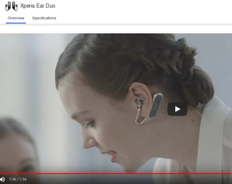
And now they're using those FD-SOI chips in audio applications. You'll find it in the Xperia™ Ear Duo, he said. The MWC press release noted that Xperia Ear Duo “... is driven by Sony’s ultra-low power consuming “CXD5602” chip and a sophisticated multi-sensor platform, the “Daily Assist” feature will recognize time, location and activities to offer relevant information throughout the day – reminding you what time your next meeting is when you reach the office or narrating the latest news headlines.”
Also in that PR, Hiroshi Ito,Deputy Head of Smart Product Business Group at Sony Mobile Communications, said, “Ear Duo is the first wireless headset to deliver a breakthrough Dual Listening experience – the ability to hear music and notifications simultaneously with sounds from the world around you.” The highly anticipated wireless “open-ear” stereo headset started rolling out to select markets in Spring 2018. There's a great info page with video here.
https://youtu.be/1lKo9acJDPs
So that's what we heard in the morning. My next post (or posts?) will cover the afternoon. That includes Dan Hutcheson's excellent talk updating his FD-SOI survey, presentations from Samsung, Globalfoundries and Simgui, plus some from very cool start-ups, and the final panel presentation.