downloadGroupGroupnoun_press release_995423_000000 copyGroupnoun_Feed_96767_000000Group 19noun_pictures_1817522_000000Member company iconResource item iconStore item iconGroup 19Group 19noun_Photo_2085192_000000 Copynoun_presentation_2096081_000000Group 19Group Copy 7noun_webinar_692730_000000Path
Skip to main content
Default Banner Image

Soitec

Excellent news and exciting applications made headlines at the recent FD-SOI and RF-SOI events in Shanghai. During the FD-SOI day, Amazon/Blink and Intellifusion shared news about their new chips, and we got updates from GF and Samsung. The RF-SOI day featured a great talk with details about China Mobile's 5G plans, and peeks at Nokia's groundbreaking approach and Qorvo's outlook. [caption id="attachment_12354" align="alignright" width="300"] (Photo courtesy: Verisilicon)[/caption] The hall was absolutely full – with over 300 people attending each day. The FD-SOI event was by invitation only, and there were far more people wanting to attend than there was room for, even given the big room in which the events were held. The events got excellent coverage in the China tech press. For example, EEWorld started with an overview article and added five supporting pieces zooming in on key presentations and companies: one on GlobalFoundries, one on Samsung, one on Verisilicon, and two on Soitec (CEO and top exec interviews). These pieces are in Chinese, but just open the links through your favorite translation site. Many of the key slides are captured in these articles, so if you can't wait for the ppts to be posted on the SOI Consortium website, you can get some quick previews now. The Verisilicon PR folks also wrote up highlights of the FD-SOI event in real time with lots of great pictures – you can read that here. Many thanks to that team, too, for flagging the coverage in the China press and posting it on their WeChat account. On the RF-SOI side, the Simgui folks wrote that up – you can read it here. They also sponsored a gala dinner with awards given to Qorvo and SmarterMicro – you can read about that here. Most of the presentations will be posted on the SOI Consortium website over the next few weeks, at which point we'll cover them in-depth here at ASN. But for now, here's a quick round-up of some of the highlights. FD-SOI Highlights [caption id="attachment_12347" align="alignright" width="300"] (Courtesy: Blink, Verisilicon)[/caption] Boston-area based Blink, which makes very popular home security systems, was recently bought by Amazon (see their current product page here). They just taped out a new chip on Samsung's 28FDS FD-SOI technology, and they're really happy about it. “I believe for battery powered devices at home, FD-SOI is the way to go,” said Yantoa Jia, Head of ASIC China Ops at Blink. Their goal in the move from 55nm bulk to 28nm FD-SOI was to double battery life, add features and control costs: and they did it. Even adding two more CPU cores and lots more features, “The power drop is fantastic,” he said. Design was no problem, he continued, and there was plenty of IP. Once the new generation is officially announced, he promised to sit down with ASN and give us more details. Attendees also heard about a new chipset from Intellifusion, which is putting its face recognition technology onto GlobalFoundries' 22FDX FD-SOI with design house Verisilicon. CEO Nin Chen gave an impromptu talk about how their technology is used to find missing people and property. The new chip, which is especially designed for use in cities, is network-to-cloud leveraging AI. For his part Thomas Morgenstern, GlobalFoundries SVP and GM of the Dresden Fab 1, said they're seeing high yields and increasing capacity for 22FDX. The marketing and manufacturing ecosystem has been built around the fab in Europe. Now, he said, the key is to build an FD-SOI ecosystem in China. The market needs of China largely parallel those of Europe, he noted, for performance and efficiency at the right cost point. The ecosystem enables fast time-to-market and 1st-time-right. [caption id="attachment_12343" align="alignleft" width="300"] (Photo courtesy: Cadence)[/caption] Samsung SVP Gitae Jeong sees their FD-SOI technology as the right solution for the 4th Revolution, which includes everything from energy harvesting to self-driving cars. They've just taped out their first 5G mmWave cellular chip on 28FDS, he revealed. eMRAM is looking very good, only requiring three additional masks and getting stable yields from -40o to 105oC. 18FDS is on schedule, with PDK 0.5 now being released, and 1.0 on track for release in March 2019. They expect a very fast ramp, and are looking at a 35% area reduction, power cut in half and performance up 22% compared to 28FDS. RF-SOI Highlights [caption id="attachment_12350" align="alignright" width="300"] China Mobile, Project Manager Danni Song (Photo courtesy: Simgui)[/caption] When China Mobile talks, the world listens. Project Manager Danni Song presented again this year (she gave a great talk last year, too). China has a very ambitious 5G project underway, and under two years in which to roll it out. The biggest challenges are power consumption and cost (a problem made worse by the additional power amplifiers needed for MIMO). Can RF-SOI help solve these challenges, she asked? One thing she did clarify during the panel discussion was with respect to the mmWave part of the 5G puzzle. Their initial 2020 rollout will only focus on sub-6GHz, with mmWave following a year or two later. Michael Reiha, Head of RFIC R D at Nokia Mobile Networks clarified the worldwide 5G rollout during the panel discussion. Different locations on the planet have different histories and needs, so will rollout 5G in different ways. For historical reasons (and a lack of choice), the US will lead with mmWave, he said. Europe, meanwhile, will focus on 24GHz to meet the needs of automotive radar. In his presentation, Reiha described Nokia's approach to power amplifiers (PA), which is very different from what others are doing. With RF-SOI, he said, you can add sensors and logic for a level of preventative care, so you can gauge and protect your equipment using AI. He believes this disruptive approach will put them two years ahead of the industry, enabling massive MIMO to be deployed in dense urban areas with 60% lower power consumption and 50% savings in material costs. Go read about their Reefshark tech, he urged, which he says will beat GaAs. “The future is very bright with RF-SOI,” he concluded. “I can state that with confidence.” [caption id="attachment_12351" align="alignleft" width="300"] Julio Costa, Director of Technology Development, Qorvo (Photo courtesy: Simgui)[/caption] Julio Costa, Director of Technology Development at Qorvo sees it differently. Traditionally a GaAs house, all their RF-SOI work is fabless. While RF front end modules (FEMs) are loaded with RF-SOI, he said, and are a big winner for antenna tuning, Qorvo still sees GaAs for high-efficiency amplifiers and envelope tracking. But, he said, it will be a battle. GaAs wins in terms of area and power consumption he contends, but adds that SOI wins in terms of cost. Power levels, he predicts, will be the determining factor. So that's the quick overview – we'll drill down into the presentations as they're posted, so stay tuned!
Read More
The presentations from the SOI Consortium sponsored workshop held during Semicon West are now posted and freely available on the website – click here to see the full agenda with links to the presentations. The workshop, entitled 4G/5G Connectivity: Opportunities for the SOI Supply Chain, was well-attended and generated excellent discussions. If you don't have time to look at all of the ppts, here are quick overviews. Market Overview and FD SOI Opportunities, by Handel Jones, CEO, IBS. Handel Jones is an industry veteran, China expert and longtime follower of the SOI ecosystem. High performance with low power consumption are the key requirements for the continued growth in the semiconductor industry, he said, making FD-SOI the right choice for a wide range of products. Here's how he sees it: [caption id="attachment_12312" align="alignleft" width="300"] (Courtesy: IBS and SOI Consortium)[/caption] He estimates the yearly TAM (total available market) for FD-SOI based products in the range of $46 billion over the next 10 years, largely driven by needs for ultra-low power and RF integration. He goes on to break out volumes by applications (including ISPs – image signal processors; and CIS – CMOS image sensors), foundry markets by feature dimension and to map out technology trends. Mobile Radio Transformation in the Age of 5G: A Perspective on Opportunities for SOI, Peter Rabbeni, Vice President, Globalfoundries. Peter Rabbeni is an RF expert par excellence, having overseen the shipping of over 35 billion RF-SOI products to date. In his presentation, he details how 5G NR (New Radio) sub-6GHz frequency band specifications significantly increase frequency range and channel bandwidth, and how new band support and MIMO complexity and die size per handset are driving complexity in RF FEMs. Furthermore, 5G/mmWave phased arrays are driving a paradigm shift in the approaches that can be taken, he explains, so greater integration is needed. Here's a great slide showing where GF's two main SOI technologies come into play: [caption id="attachment_12311" align="alignleft" width="1000"] (Courtesy: GlobalFoundries and SOI Consortium)[/caption] Empowerment of 5G with SOI-Based Technologies, Emmanuel Sabonnadière, CEO, Leti-CEA. [caption id="attachment_12310" align="alignleft" width="300"] (Courtesy: Leti and SOI Consortium)[/caption] Working in partnership with industry leaders around the world, Leti has been the research powerhouse behind all things SOI since the early 1980s. In fact Reuters ranks them #2 in their most recent list of the World’s Most Innovative Research Institutions. This presentation reviews the key technical benefits of FD-SOI for IoT and IMT (that's international mobile communications, btw). Engineered Substrates – at the Foundation of 5G, Thomas Piliszczuk, Executive Vice President, Soitec. This presentation really puts the context around engineered substrates. Here are two excellent and useful slides here that identify which engineered substrates go where in the 5G world, and the engineered substrates that Soitec provides. Check these out: [caption id="attachment_12309" align="alignleft" width="1000"] (Courtesy: Soitec and SOI Consortium)[/caption] [caption id="attachment_12308" align="alignleft" width="1000"] (Courtesy: Soitec and SOI Consortium)[/caption] Ultra-thin Double Layer Metrology with High Lateral Resolution, Bernd Srocka, Vice President, Unity GmbH. [caption id="attachment_12307" align="alignleft" width="300"] (Courtesy: Unity and SOI Consortium)[/caption] In case you're not familiar with them, Unity provides a wide range of solutions in metrology and inspection. Both the top silicon layer and BOX layer of wafers for FD-SOI applications have draconian requirements that have required new approaches in metrology to ensure the thickness and homegeneity control of these very thin layers. China 5G Plan and SOI Ecosystem, Jeffrey Wang, CEO, Simgui. Shanghai-based Simgui partners with Soitec, using SmartCut™ technology for the production of RF-SOI wafers. It is doubling its capacity to reach 400K over the next year, and expanding into 300mm. China is aggressively working on 5G and plans to deploy 5G commercialization in 2020. Jeff Wang's is a terrific presentation detailing the rollout. (BTW, in addition to the massive funding effort underway, the government created the National Silicon Industry Group (NSIG) to support the semiconductor material ecosystem in China. You'll want to keep up with what's going on here). Here's the slide that summarizes the SOI ecosystem in China – the presentation then goes on to detail who does what. [caption id="attachment_12306" align="alignleft" width="1000"] (Courtesy: Simgui and SOI Consortium)[/caption] Inspection and Metrology Relevance in SOI Manufacturing, Jijen Vazhaeparambil, Vice President General Manager, KLA-Tencor. [caption id="attachment_12305" align="alignleft" width="300"] (Courtesy: KLA-Tencor and SOI Consortium)[/caption] K-T has played a strategic role in the SOI story going back for decades (and in fact they wrote a piece for the third edition of ASN back in 2005!), ensuring metrology innovations for things that hadn't previously need detection and measurement. With each new set of requirements, they rose to the occasion with wafer metrology solutions that helped increase quality and decrease costs. This presentation recaps some of them.
Read More
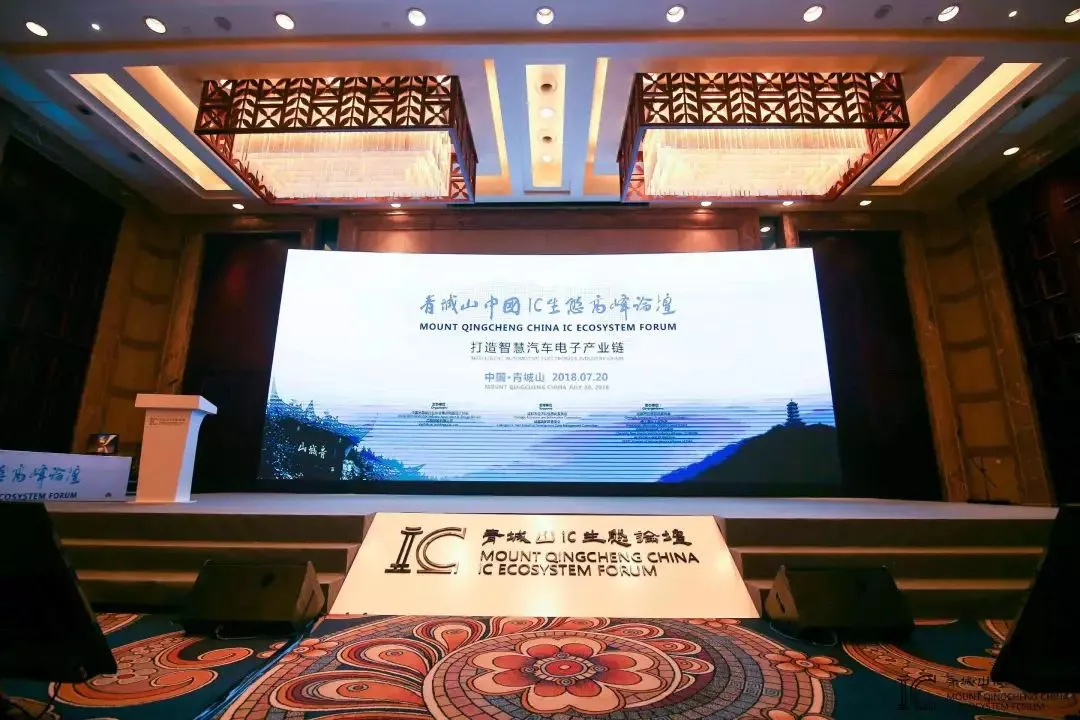
FD-SOI was a very important topic during the recent Mount Qingcheng China IC Ecosystem Forum. To situate things, Mount Qingcheng, with its lush hills and waterways, is located just outside of Chengdu. That of course is where GlobalFoundries is building its new fab, which will be the first in China to run FD-SOI. Chengdu is also a key city in China's automotive electronics landscape. [caption id="attachment_12236" align="alignright" width="300"] (Image Courtesy: VeriSilicon)[/caption] The theme of the forum was Building a Smart Automotive Electronics Industry Chain. Over 260 decision-makers from government, academia and industry attended – and the SOI Consortium had a significant presence. The event was chaired by Wayne Dai, CEO/Founder of consortium member VeriSilicon, and tireless champion of the the FD-SOI ecosystem in China and worldwide. Morning keynotes were given by: Carlos Mazure, Soitec CTO and SOI Consortium Executive Co-Director; Mark Granger, GF's VP of Automotive Product Line Management; and Tony King-Smith, Executive Advisor at AImotive, a GF 22FDX customer. BTW, transcripts of all the talks are available through Gasgoo, China's largest automotive B2B marketplace. You can click here to access them. (They're in Chinese – but you can open them in the language of your choice using the major translation websites.) Chengdu Officials Affirm Support for FD-SOI Fan Yi, Deputy Mayor of Chengdu, spoke extensively of FD-SOI in his keynote on the importance of rapidly developing smart cars. He heralded the “spectacular” new GlobalFoundries fab there. Following a meeting with the company's top brass the day before, he affirmed GF's confidence in their investment. There is a solid roadmap for FD-SOI, he noted, and efforts are underway to accelerate the move into production and expand education and training. He cited the benefits of FD-SOI for the entire supply chain, from design through package and test, raising the level of the entire IC industry to new heights. The government, he said, attaches great importance to this enterprise. Their thinking regarding intelligent transport in China is integrated with the overall approach to smart cities. SOI Consortium Leads Industry Keynotes [caption id="attachment_12232" align="alignleft" width="300"] Wayne Dai, VeriSilicon Founder and CEO (Photo courtesy VeriSilicon)[/caption] In his opening remarks, Wayne Dai emphasized the need for China to seize the advantage in the next round of development opportunities in the automotive electronics industry. This year's Qingcheng forum, he noted, brought together key representatives from across the supply chain, from of the highest to the deepest reaches of the smart car electronics industry, and across markets, technologies, solutions, industrial ecosystem, standards and regulations. In his talk on how FD-SOI is boosting the accelerated development of automotive electronics, Carlos Mazure presented the SOI Industry Consortium. He noted that the Consortium promotes mutual understanding and development across the ecosystem. SOI is already present throughout automotive applications, he noted. There are currently about 100mm2 of SOI per car, in such diverse areas power systems, transmissions, entertainment, in-vehicle networking and more. SOI will experience especially high growth in electrification, information/entertainment, networking, 5G, AI/edge computing and ADAS. He then went on to give some history and an extensive overview of the major trends and highlights we've seen over recent years. He finished by giving examples of convergence across the supply chain with IC manufacturers working with automakers to lower power, increase processor performance and advance 5G. [caption id="attachment_12233" align="alignright" width="665"] Carlos Mazure, Soitec CTO and SOI Consortium Executive Co-Director; Tony King-Smith, Executive Advisor at AImotive and Mark Granger, GF's VP of Automotive Product Line Management (Photo courtesy VeriSilicon)[/caption] GF's Mark Granger addressed the rapid development of automotive electronics. In certain areas, he said, he sees growth rates of over 20%. They are working on building the Chengdu ecosystem, especially for design, and in cooperation with the rest of the supply chain. Furthermore, he reminded the audience, when you talk about cars, travel implies that you also talk about IoT as well as things like infotainment and integrated radar ICs. In addition to cost and power efficiencies, the AEC-Q100 standard for IC reliability in automotive applications is also pushing designers to turn to FD-SOI. In the GF meeting with Chengdu government officials (referenced above in deputy mayor Fan Yi's talk), he too confirmed their support of FD-SOI as a key technology for China. GF is currently cooperating with about 75 automotive partners, he said, and the company is looking to increase cooperation with partners in the Chengdu region. Tony King-Smith talked about the 22FDX test chip AImotive is doing with Verisilicon and GF. In case you missed it, in June 2017 AImotive announced its AI-optimized hardware IP was available to global chip manufacturers for license. AiWare is built from the ground up for running neural networks, and the company says it is up to 20 times more power efficient than other leading AI acceleration hardware solutions on the market. In the same announcement, they revealed that VeriSilicon would be the first to integrate aiWare into a chip design,and that aiWare-based test chips would be fabricated on GF's 22FDX. The chip is expected to debut this year. While the afternoon agenda was not specific to FD-SOI, it did focus on the "smart cockpit" and "intelligent driving", with talks by nine leading players in China's automotive IC and investment communities. ~ ~ ~Note: Many thanks to the folks at VeriSilicon, who wrote up this event for their WeChat feed, and shared photos with us here at ASN.
Read More
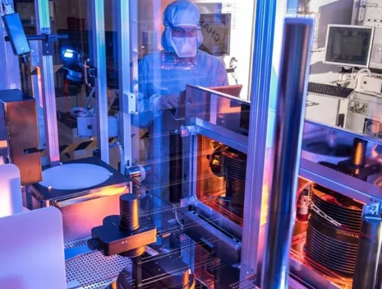
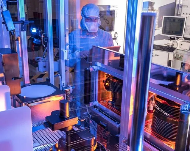
Specialty foundry TowerJazz is ramping a 65nm version of its RF-SOI process on 300mm wafers at Fab 7 in Uozu, Japan. To support the ramp, the company has signed a contract with long-term partner, Soitec, guaranteeing a supply of tens of thousands of 300mm SOI silicon wafers, securing wafer prices for the next years and ensuring supply to its customers, despite a tight SOI wafer market. [caption id="attachment_12108" align="alignright" width="300"] The 300mm 65nm RF-SOI process will be offered at the Uozu, Japan fab, which is operated by the TowerJazz Panasonic Semiconductor Company (TPSCo). (Photo courtesy: TowerJazz)[/caption] Five of TJ's seven fabs do RF-SOI. LNA (low-noise amplifers) are a big market driver, and with RF-SOI they can integrate the LNA with the switch, CEO Russell Ellwanter said in his lead keynote at the SOI Consortium’s 5th International RF-SOI Workshop in Shanghai (spring, 2018). BTW, that was in fact a very inspirational talk about Value Creation, and the importance of treating your suppliers with respect. He credited his company’s close relationship with RF-SOI wafer-supplier Soitec for TJ’s claim to the world’s best linearity. “We are delighted to see the strong adoption of 300mm RF SOI through this large capacity and supply agreement with TowerJazz to augment our already significant 200mm RF-SOI partnership,” said Soitec CEO Paul Boudre. “TowerJazz was the first foundry to ramp our RFeSI products to high volume production in 200mm and continues as one of the industry leaders in innovation in this exciting RF market with advanced and differentiated offerings.” According to the TJ press release (you can read it here), with its best in class metrics the TowerJazz 65nm RF-SOI process enables the combination of low insertion loss and high power handling RF switches with options for high-performance low-noise amplifiers as well as digital integration. The process can reduce losses in an RF switch improving battery life and boosting data rates in handsets and IoT terminals. It's a high-growth market, to be sure. Market researchers Mobile Experts predict that the mobile RF front-end market will reach $22 billion in 2022 from an estimated $16 billion in 2018. TowerJazz says its breakthrough RF SOI technology continues to support this high-growth market and is well-poised to take advantage of next-generation 5G standards, which will boost data rates and provide further content growth opportunities in the coming years. Customers are already getting into position. For example, Maxscend (WuXi, China), a provider of RF components and IoT integrated circuits, is ramping in this new technology. “We chose TowerJazz for its advanced technology capabilities and its ability to deliver in high volume while continuously innovating with a strong roadmap. We specifically selected its 300mm 65nm RF SOI platform for our next-generation product line due to its superior performance, enabling low insertion loss and high power handling,” said Maxscend CEO Zhihan Xu. As longtime ASN readers will know, we've been covering the evolutions of TJ's RF-SOI platforms since the beginning of the decade. It's worth noting, too, that beyond RF, TowerJazz also offers foundry customers other SOI-based processes, such as the new 0.18μm BCD SOI, a 200V SOI technology platform (announced in 2017, press release here) for motor drivers, industrial tools, electric vehicles and more. The previous generation 0.18μm SOI for automotive power management also offers exceptional area savings and is well-suited for high temperature operation. Back in 2014, here at ASN we did a great interview with TJ SVP Dr. Marco Racanelli about when and why they use SOI – and while processes have advanced, the basic drivers are still there, so it's a still a good read. And finally, designers will want to know that the TJ Multi-Project Wafer (MPW) Shuttle Program offers the 65nm RF-SOI process, as well as other SOI-based processes. See the website for scheduling and details.
Read More
Leti and Soitec have announced a new collaboration and five-year partnership agreement to drive the R D of advanced engineered substrates, including SOI and beyond. This agreement brings the traditional Leti-Soitec partnership to a whole new dimension and includes the launch of a world-class prototyping hub associating equipment partners to pioneer with new materials, The Substrate Innovation Center will feature access to shared Leti-Soitec expertise around a focused pilot line. Key benefits for partners include access to early exploratory sampling and prototyping, collaborative analysis, and early learning at the substrate level, eventually leading to streamlined product viability and roadmap planning at the system level. [caption id="attachment_12066" align="aligncenter" width="644"] CEOs Emmanuel Sabonnadière (Leti) and Paul Boudre (Soitec) announcing the new Substrate Innovation Center during Semicon West '18. (Image courtesy: Leti)[/caption] Leading chip makers and foundries worldwide use Soitec products to manufacture chips for consumer applications targeting performance, connectivity, and efficiency with extremely low energy consumption. Applications include smart phones, data centers, automotive, imagers, and medical and industrial equipment, but this list is always growing, along with the need for flexibility to explore new applications starting at the substrate level. At the Substrate Innovation Center, located on Leti’s campus, Leti and Soitec engineers will explore and develop innovative substrate features, expanding to new fields and applications with a special focus on 4G/5G connectivity, artificial intelligence, sensors and display, automotive, photonics, and edge computing. “Material innovation and substrate engineering make entire new horizons possible. The Substrate Innovation Center will unleash the power of substrate R D collaboration beyond the typical product road maps, beyond the typical constraints,” said Paul Boudre, Soitec CEO. “The Substrate Innovation Center is a one-of-a-kind opportunity open to all industry partners within the semiconductor value chain.” Whereas a typical manufacturing facility has limited flexibility to try new solutions and cannot afford to take risks with prototyping, the mission of the Substrate Innovation Center is to become the world’s preferred hub for evaluating and designing engineered substrate solutions to address the future needs of the industry, inclusive of all the key players, from compound suppliers to product designers. Using state of the art, quality-controlled clean room facilities, and the latest industry-grade equipment and materials, Leti and Soitec engineers will conduct testing and evaluation at all levels of advanced substrate R D. “Leti and Soitec’s collaboration on SOI and differentiated materials, which extends back to Soitec’s launch in 1992, has produced innovative technologies that are vital to a wide range of consumer and industrial products and components,” said Emmanuel Sabonnadière, Leti CEO. “This new common hub at Leti’s campus marks the next step in this ongoing partnership. By jointly working with foundries, fabless, and system companies, we provide our partners with a strong edge for their future products."
Read More
“GlobalFoundries, TowerJazz, TSMC and UMC are expanding or bringing up RF SOI processes in 300mm fabs in an apparent race to garner the first wave of RF business for 5G, the next-generation wireless standard,” writes Mark Lapedus of Semiconductor Engineering. His recent piece, RF-SOI Wars Begin, explains why demand across the supply chain is currently tight. Rest assured, the supply situation is being addressed fast. By next year, 300mm-based RF-SOI manufacturing (vs. 200mm) will increase from 5% to 20%. But with insatiable end-user demand for greater throughput, overall RF-SOI device demand is increasing in the double-digit range, so 200mm-based manufacturing is also expanding fast. [caption id="attachment_11905" align="alignleft" width="300"] The front-end modules in all smartphones are built on Soitec's RF-SOI wafer technology. The most advanced, for LTE/LTE-A, are built on Soitec's RFeSI-SOI wafers, which have four layers to meet the demands of devices with high linearity requirements. (Courtesy: Soitec)[/caption] SOI wafer manufacturer Soitec has 70% of the RF-SOI wafer market share. The other RF-SOI wafer manufacturers – Shin-Etsu, GlobalWafers and Simgui – all use Soitec's RF-SOI wafer manufacturing technology. This is an excellent, comprehensive piece, that clearly explains the complexities of the markets, the devices, the manufacturing and the supply chain. It's a highly recommended read. BTW, the SOI Consortium is organizing a 4G/5G SOI supply chain workshop during Semicon West (July '18). Sign up or get more information on that under the Events tab here on the consortium website. Of course, here at ASN, we've been covering RF-SOI for over a decade. You can use our RF-SOI tag to access most of the pieces we've done over the years.
Read More
Good news: there are far fewer bigoted extremists out there when it comes to FD-SOI vs. FinFETs. People want the best technology for their application. It's that simple. That's a key piece of news from the updated survey by Dan Hutcheson, CEO of VLSI Research, which he presented in the afternoon session of the SOI Consortium's 2018 SOI Symposium in Silicon Valley The afternoon then featured presentations by foundry partners, which I'll cover here. Also in the afternoon were presentations by wafer-maker Simgui, some innovative start-ups leveraging FD-SOI for custom SoCs and the final panel discussion. I'll cover those in Part 3 of this series. BTW, if somehow you missed my coverage of the morning sessions about very cool new products and projects from NXP, Sony, Audi, Airbus and Andes Technology, be sure to click here to read it. The presentations are starting to be posted on the SOI Consortium Events page – but some won't be. Either way, I'll cover them here. VLSI Research A couple years ago at the annual SOI Symposium in Silicon Valley, Dan Hutcheson presented results of a survey he did (ASN covered it – you can still read about it here). At the 2018 event, he presented an update, which is now posted. You can get it here. The FD-SOI roadmap and IP availability are no longer issues for decision makers, he found. The 14nm branch – do you go FinFET or FD-SOI? – is gone. “Fins and FD are complementary,” he observed. Most people said they'd consider using both and running two roadmaps, choosing whichever technology is appropriate to a given design. [caption id="attachment_11841" align="alignnone" width="1000"] (Courtesy: VLSI Research, SOI Consortium)[/caption] From a transistor viewpoint, the top reasons to choose FD-SOI is that it's better for analog and has lower leakage/parastics. It's perceived as better for complex, high mixed-signal SoCs, and especially for RF and sensor integration. In fact, people see RF as the new mixed-signal, wherein FD-SOI is uniquely positioned for 5G and mmWave. From a business viewpoint, FD-SOI is perceived to have real advantages. In particular, FD-SOI wins when it comes to keeping down design costs, manufacturing costs and time-to-market. IoT is still the hottest target market for FD-SOI, to which he adds high growth expected in automotive and medical. Samsung With 20 tape-outs in 2018, Samsung is seeing an acceleration in its FD-SOI business. “The trend is healthy,” said Hong Hoa, SVP of the company's foundry business. FD-SOI, he continued, is on a “differentiation path.” Samsung's 28nm FD-SOI process, called 28FDS is at full maturity with very strong yields. They're seeing more customers and a wider range of applications. The design infrastructure, silicon-verified IP and methodologies are also all mature. They have optimal implementation and verification guidelines for body bias design, a body bias memory usage guide, and a body bias generator integration guide. The process supports Grade 1 automotive, and will be qualified for Grade 2 in a few weeks. FD-SOI, Hoa reminded the audience, offers superior RF performance compared to both planar bulk and 14nm FinFET. The Samsung strategy is to first provide a base for for the FD-SOI process, then add RF and eMRAM. The base for 28nm was done in 2016; they added RF in 2017 and eMRAM this year. The Samsung platform for IoT applications integrates both RF and eMRAM to support multi-function needs in a single platform. Lead customers are already working with eMRAM in their designs, he added. (BTW, Samsung has a really nice video explaining their eMRAM offering – you can see it on YouTube here.) The basic PDK for the Samsung 18nm FD-SOI process (18FDS) will be available in September 2018, with full production slated for fall of 2019. It will deliver a 24% increase in performance, a 38% decrease in power, and a 35% decrease in area for logic. RF for the 18FDSplatform will be ready by the end of this year, and eMRAM beginning in 2019. GlobalFoundries With design wins from 36 customers underway, 12 of which are taping out in 22FDX (GF's 22nm FD-SOI process) this year, the market has validated FDX for differentiation, said GF SVP Dr. Bami Bastani. And indeed, designers are using it for a wide array of applications across North America, Europe, Asia/Pacific and Japan. Customers in the North America are designing in 22FDX for NB-IoT, industrial, RF/analog, mobile, network switches and cryptocurrency applications. In Europe, it's more or less the same plus automotive/mmWave, optical transmission, wireless BTS and AI/ML. In Asia Pacific/Japan the mix is similar to Europe. Bastani sees the three big enablers as the the strengths of the roadmap, the ecosystem and multi-sourcing from Dresden and Chengdu (where they're already equipping the cleanrooms). He also tipped his hat in acknowledgment to the partnership with FD-SOI wafer supplier Soitec, noting that they have gone the extra mile to match GF's requirements. So that was the first part of a great afternoon. As mentioned above, my next post (part 3) will cover a very informative presentation by wafer-maker Simgui on the markets in China, plus talks by some innovative start-ups leveraging FD-SOI for custom SoCs and the final panel discussion.
Read More
RF-SOI innovators Jean-Pierre Raskin of UCL and Bernard Aspar of Soitec changed the course for key RF chips. The industry has long recognized their contributions: their solution for “trap-rich” RF-SOI wafers is now the starting point to virtually every FEM in every smart phone on the planet (really!). And of course here at ASN we've been following their work for over a decade. Now more accolades are coming in. The latest is the 2017 European SEMI Award, which was given at ISS Europe 2018 for “...their seminal work with radio frequency silicon-on-insulator (RF-SOI) substrates” (read the press release here). As SEMI notes, the “...award winners’ pioneering research and collaboration with academia and industry led to major advances in RF switches and ushered RF-SOI technology from concept to worldwide adoption.” Aspar and Raskin were nominated and selected by their peers within the international semiconductor community. [caption id="attachment_11677" align="alignleft" width="150"] Bernard Aspar, Executive Vice President, Communication Power BU at Soitec Aspar founded CEA-Leti spinoff Tracit Technologies in 2003. He was appointed senior vice president of the Tracit Division (now the Communication Power business unit) when Soitec acquired Tracit in 2006. He has more than 15 years of experience in direct wafer-bonding and layer transfer. Aspar has filed more than 35 patents and co-authored some 100 scientific articles. He holds engineering and Ph.D. degrees in materials sciences and a master’s degree in microelectronics from the University of Montpellier, France.[/caption] [caption id="attachment_11678" align="alignleft" width="150"] Jean-Pierre Raskin, professor, Université catholique de Louvain (UCL) Raskin contributed to pioneering scientific studies demonstrating that silicon-based MOS technology could enable affordable, high-quality mobile devices. His findings led to the advent of RF-SOI technology and today impact the global microelectronics industry. He is an IEEE Senior Member, EuMA Associate Member and Member of the Research Center in Micro and Nanoscopic Materials and Electronic Devices of the Université catholique de Louvain, where he has been a full professor since 2007. He is author or co-author of more than 350 scientific articles.[/caption] Their advanced RF-SOI technology is now behind a wide range of applications and systems in areas including mobile devices, satellite communications, IoT, automotive radar and aerospace. If you want to better understand all this, a few years ago UCL and Soitec teams contributed an excellent article to ASN. It clearly explains how and why these new substrates came to be. You can still read it here. (Or if you're still a little confused about RF-SOI vs. RF on FD-SOI, here's a piece we did back in 2015 that explains the basics.)
Read More
China Mobile is the world's largest* telco. So when Danni Song, one of the company's high-level project managers presented at the SOI Consortium's 5th International RF-SOI Workshop in Shanghai, you can bet people listened. With each new slide, a glowing sea of cell phone cameras rose over the heads of the audience in the huge, packed ballroom. [caption id="attachment_11612" align="alignleft" width="300"] (Photo courtesy: SOI Consortium, Simgui)[/caption] Over the last month, there's been a lot more coverage of 5G in the press (especially after the recent Mobile World Congress (MWC) – check out Junko Yoshida's EETimes piece for example). For ASN readers who want to know more about 5G and RF-SOI in China, here's a reminder that Song's presentation, and many of the others given by leading companies at the RF-SOI Workshop last fall, are now posted on and freely available the Consortium website Events page. Click here for the listing and links.The theme of the workshop was IoT, mobile, 5G connectivity, and mmW. As Dr. Xi Wang, Director General of SIMIT/CAS (the Shanghai Institute of Microsystem Information Technology in the Chinese Academy of Sciences), said in his opening keynote, China is strong in RF-SOI. RF-SOI will be growing at a CAGR of over 15% for the next five years, and China has production, design, wafer manufacturing and good momentum. “We will make a great contribution to the whole IC industry,” he predicted.Of note, too, Russell Ellwanter, CEO of TowerJazz, gave what turned out to be a very inspirational keynote about Value Creation, and the importance of treating your suppliers with respect. He credits his company's close relationship with RF-SOI wafer-supplier Soitec for TJ's claim to the world's best linearity. Five of their seven fabs do RF-SOI. LNA (low-noise amplifers) are a big market driver, and with RF-SOI they can integrate the LNA with the switch.Here are some more highlights from the day – but by all means check out the presentations for details. (You can click on the illustrations to see them in full screen.)China MobileIn her presentation, Embrace a Brand New Cooperation in 5G Era, Song asked where RF-SOI could help in her wish list. Could it increase integration and decrease cost and power consumption? Can it help improve NB-IoT device performance? The supply chain needs to come back around into a circle, so that the telcos are connected to and get insights from the wafer substrate providers, she said. [caption id="attachment_11608" align="alignright" width="300"] (Courtesy: China Mobile, SOI Consortium)[/caption] China Mobile has a 5G Innovation Center, and has established test labs in 8 cities. And the government has announced a 5G launch in 2020, with pre-commercial trials now going into 20 cities. So she was at the RF-SOI Workshop as much to listen and learn as to share China Mobile's vision.Sony [caption id="attachment_11613" align="alignleft" width="300"] (Courtesy: SOI Consortium and Sony)[/caption] The presentation by Kidetoshi Kawasaki, GM of Sony Semiconductor Solutions, focused on antenna tuning, which he said is one of the fastest growing things in cell phones. Antenna Tuning Progress SOI Single Chip Integration for 4G/5G UE (note that UE = user equipment) looks at antenna aggregation, and why it is important for carrier aggregation (CA) and MIMO. Sony has developed an SOI-based next-gen process for 5G integrating passive components. That's why RF-SOI is important and will be continued to be used in the mobile market, he said.GlobalFoundriesGF has developed demo vehicles to help customers, said Sr. Director of the RF Business Unit, Peter Rabbeni. (Over the years they've shipped over 32 billion RF-SOI devices, btw.) In his presentation, RF-SOI: Delivering Performance Integration for the Next Generation of Mobile,he noted that RF is becoming more complex than digital. As a result there is a need to integrate to help reduce cost: this is a direct correlation to the standards that are driving complexity. At the same time, performance requirements are increasing, so the challenge is driving increased performance at the same or lower cost than previous generations of products. [caption id="attachment_11609" align="alignright" width="300"] (Courtesy: GlobalFoundries and SOI Consortium)[/caption] To meet 4G/LTE and 5G's evolving performance demands, GF has recently introduced two new RF-SOI platforms, which he detailed in the presentation. 8SW enables increased integration of front-end modules (FEMs), while 45RFSOI is for mmWave FEMs. (In a separate presentation, IDDO-IC CEO Denis Masliah presented a Differential Complementary Millimeter Wave Power Amplifier for 5G using 45RFSOI process, which is currently being fabbed by GF.)RF-SOI Wafer SuppliersThe two leading RF-SOI wafer suppliers, Soitec and partner Simgui, both gave excellent presentations. Though Soitec EVP Bernard Aspar's presentation Engineered Substrates as Foundation of Innovation in RF is not posted, he made some important points. Up til now, RF-SOI has mainly been about switches and tuners, he said, but there are other opportunities that offer the potential for huge growth. The full supply chain needs to be prepared, he said, and suppliers need to understand each other. Each technology requires the right substrate – and even as we move into sub-6GHz 5G, there is still work to be done in 4G. In fact Soitec is now offering services to help customers better understand new substrate options. [caption id="attachment_11611" align="alignright" width="300"] (Courtesy: Simgui, SOI Consortium)[/caption] Soitec's partner in China, Simgui, now uses Soitec's Smart CutTM technology for RF-SOI wafer production. Together the two are now producing over a million 200mm RF-SOI wafers/year, said Simgui Sr. Director, Kerui Wang. His presentation, RF-SOI – a Secured Substrate Supply Chain, looked at their strategic partnership with Soitec, wherein they use the same tools and processes to deliver the same products meeting the same specs.Fabs and FablessTwo leading fabless companies – RDA Microelectronics (which was acquired by Spreadtrum) and SmarterMicro also presented their RF-SOI activities. Although their ppts are not posted, here are a few highlights.Longtime ASN readers will recall that RDA has been shipping high-volume, RF-SOI based chips to Samsung and others for over five years. In the presentation, RF-SOI in Current and Future RFFE Solutions, Engineering AVP Joseph Jia said that over last two years alone they've released almost 50 RFFE (front end) chips on RF-SOI. They see RF-SOI as the right match for switches, tuners and NB-IoT because of the low-voltage and tunability advantages.SmarterMicro's CTO, Peter Li, sees RF-SOI as a cornerstone of 5G. In his presentation, Reconfigurable RFFE in 5G, he said the goal is smart systems on fewer dies to decrease size and cost.Jeff Zhu, assistant director at SMIC, presented SMIC, 0.13um RF-SOI Platform Updates. Mainland China's largest foundry has recently moved its RF-SOI process from 180 to 130um, and he walked us through some chip designs.Throughout the day, presenters noted that RF is a great opportunity for China to take a leadership position. As one panelist at the end of the day noted, RF depends more on expertise and talent than digital, which depends more on manpower.Nanjing: A China RF CapitalJust before the Shanghai events, there was a 2-day event sponsored by the City of Nanjing, co-organized by SOI Industry Consortium and the City of Nanjing. Over 200 participants attended the workshop and tutorials on SOI applications, SoC development and manufacturing, EDA IP ecosystem, as well as a design tutorial for More than Moore SOI ecosystem. Almost all of those presentations are now posted on the Consortium – click here to get them.Some of the participants in the SOI Consortium's delegation also had the opportunity to visit the enormous Nanjing Sofware Park. Nanjing, we learned, is often considered China's “RF capital”. The list of the world's major RF players working in partnership there is certainly an international who's who.So, lots of good RF-SOI/5G info on the SOI Consortium website – check it out!~ ~ ~*in terms of market value and subscribers.
Read More