downloadGroupGroupnoun_press release_995423_000000 copyGroupnoun_Feed_96767_000000Group 19noun_pictures_1817522_000000Member company iconResource item iconStore item iconGroup 19Group 19noun_Photo_2085192_000000 Copynoun_presentation_2096081_000000Group 19Group Copy 7noun_webinar_692730_000000Path
Skip to main content
Default Banner Image

GF

Some really innovative start-ups presented chips they're doing on FD-SOI at the SOI Consortium’s 2018 SOI Symposium in Silicon Valley. We'll cover those here in Part 3 of ASN's coverage, as well as a presentation on China by wafer-maker Simgui and the final panel discussion. BTW, if somehow you missed my coverage of the morning sessions about very cool new products and projects from NXP, Sony, Audi, Airbus and Andes Technology, be sure to click here to read it. And in the afternoon the foundry partners provided excellent insight into who's designing chips on FD-SOI, and VLSIresearch explained why. You can read that here. Some of the presentations are posted on the SOI Consortium Events page – but some won’t be. Either way, I’ll cover them here. Start-upsIneda Systems began as an ADAS start-up, and are now working on developing low-power SoCs for use in consumer and enterprise applications. They're using FD-SOI for their current family of chips. SVP Ramkumar Subramanian emphasized that NRE costs are really important for smaller designs. 22FDX, he said, enabled them to move from 40nm, and ramp to larger volumes. In February, GreenWaves Technologies, a fabless semiconductor startup designing disruptive ultra-low power embedded solutions for image, sound and vibration AI processing in sensing devices, announced its GAP8 IoT application processor. GAP8 evaluation boards can now be ordered. The GAP8 agile power management architecture combined with IOT low duty cycling is a perfect fit for FDSOI processes. CEO Loic Lietar talked about how it would be used in AI applications at the very edge, wherein only the necessary data should be uploaded to the cloud. Also in February, Dream Chips’ announced that its ADAS SoC fabbed in GlobalFoundries’ 22FDX (FD-SOI) technology was posting record power efficiency (you can read more about it in ASN's coverage at the time here.) Dream Chips is Germany’s largest independent Engineering Service Provider. At the symposium, CEO Jens Benndor's talked about their roadmap. [caption id="attachment_11865" align="alignleft" width="300"] (Courtesy: eVaderis, SOI Consortium)[/caption] eVaderis CEO Jean Pascal Bost talked about how data-intensive IoT applications are enabled with FD-SOI and embedded magnetoresistive non-volatile memory (eMRAM) technology. You can get the slides from his talk here. eVaderis has eflash-like and eSRAM-like eMRAM IP that covers most MCU applications. They also have an eMRAM compiler tool and high-value-added IP for 22FDX. They foresee impressive power savings at the system level with body biasing: 25x this year and up to 45x in 2020, so that intelligence can be brought to IoT. In February they announced that they are co-developing an ultra-low power MCU reference design using GF’s eMRAM technology on the 22FDX® platform. And in March eVaderis and Mentor/Siemens announced that eVaderis proprietary Magnetic Tunnel Junction (MTJ) model would be co-optimized with AFS to speed-up simulations and generations of embedded MRAM IPs and compiler products with good accuracy.An 22FDX MCU reference design project is underway, with tape-out in July '18. Reduced Energy Microsystems (REM) CEO William Coven talked about realizing near-threshold computing with 22FDX and low-power memories. REM has two products on 22FDX: their Neuron Vision SoC and 64-bit RISC-V IP cores. 22FDX, he says, has been fantastic. Simgui Jeffrey Wang, the CEO of wafer-maker Simgui looked at why China is promoting its IC industry. (In the SOI ecosystem, Simgui is particularly known for its RF-SOI wafers, which it produces using Soitec's Smart CutTM process.) This was more of an overview talk, not necessarily specific to the SOI ecosystem, but certainly interesting. In terms of worldwide semiconductor sales, he said, about half end up in China. The CICF – aka the Big Fund – is currently running at about $74 billion. Having realized that mergers acquisitions would not solve the problem, they've opened a second round, targeting another $160 billion. China's two biggest innovation success stories are Huawei (with its Kirin processor), and China Rail, which is now a global Fortune 500 company. The CAGR for the China semiconductor industry is 19%, though they need 20% to reach their goals. IC design is a particularly successful area, posting a CAGR of 29%, with two players in China in the top 10 worldwide. Packaging and assembly/test are also very strong. Zing is working on increasing the supply of 300mm silicon wafers, while Simgui is expanding in both 200 and 300mm capex, due to “big demand”, he said. Panel Discussion [caption id="attachment_11866" align="alignleft" width="300"] SOI Symposium Panel Discussion: (left to right): Giorgio Cesana (Co-Director SOI Consortium), Dave Eggleston (VP GF), Tim Saxe (CTO, Quicklogic), Wayne Dai (CEO, Verisilicon), Samir Patel, (CEO Sankalp Semi), Kelvin Low (VP, ARM), Mahesh Tirupattur (EVP, Analog Bits)[/caption] The day wrapped up with an excellent panel discussion moderated by SOI Consortium Executive Co-Director Giorgio Cesana. Here are a few of the observations made by the panelists. QuickLogic CTO Tim Saxe said that FD-SOI made their designs more compact. With FD-SOI for FPGAs, you've got one set of IP, and you can decide at runtime where you're going for low power or high performance. With a lot of power domains, you see the benefits at the system level. GF VP Dave Eggleston said they're seeing early adopters of eMRAM, especially for wearables with RF and low power. ARM VP Kelvin Low said people should do more than just migrate to FD-SOI. If they use back biasing, it can replace the need for big/little cores. Body biasing makes things easier, maintained Verisilicon CEO Wayne Dai. His teams find that with body biasing, you can tape out for “typical” instead of “worst case”. It's not too late for FD-SOI: it's perfect timing for the MCU market, which is still at 40nm, said Sankalp Semi CEO Samir Patel. As designers, they're happy to focus on companies still on the older nodes. The IP ecosystem should be more enthusiastic about FD-SOI, said Analog Bits EVP Mahesh Tirupattur. You've got more potential customers, and your volume runs can be bigger. In his closing remarks, SOI Consortium Executive Co-Director Carlos Mazure reminded the audience of the day's three take-aways: power consumption is driving even systems companies FD-SOI is penetrating fields like MCUs and SoCs where more intelligence is needed China is still a really big opportunity.
Read More
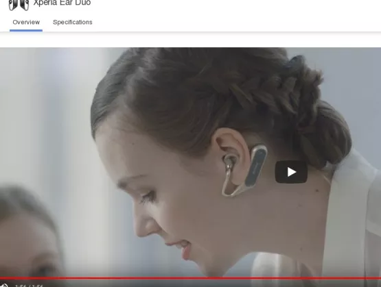
“The ecosystem is ready. The focus is now on applications and products.” And with those words, SOI Consortium Executive Director Carlos Mazure opened the annual Silicon Valley SOI Symposium. As promised, the day was packed with presentations about products on FD-SOI – some from big players like NXP and Sony, some from names new to the FD-SOI ecosystem like Audi and Airbus, and some from start-ups just getting into the game. The event got excellent coverage in EETimes/EDN – including in their editions across the globe in China, Japan, Taiwan, India and more. Samsung, GF Ramp FD-SOI, heralded the headlines. It was a full day of excellent presentations. In this post, I'll chronicle the morning presentations. The next post(s) will cover the afternoon session. Note that as of this writing, the ppts are not yet posted on the SOI Consortium website, but many will be. Keep checking back under the Events tab, and look under “past Events”. Andes Technology As semiwiki noted a few years back, Andes Technology is “...the biggest microprocessor IP company you've never heard of.” Based in Taiwan, Mediatek is one of their big customers; they've got a strong client base across Asia/Pacific, and are now making inroads into North America. Last year they announced with GF their 32-bit CPU IP cores had been implemented on GF's 22FDX® FD-SOI technology. In his symposium keynote, CEO Frankwell Lin said that in the test chip they're doing with GF and Invecus, they're seeing a 70% power savings compared with what they'd gotten in 28ULP. Their newest products are the N25 32bit and NX25 64bit RISC-V based cores, and in July they'll announce a core that runs on Linux. NXP “With FD-SOI we're enabling the future of embedded processing,” the always-quotable (and keynote speaker) NXP VP/GM Ron Martino told us. NXP's i.MX7ULP, i.MX8, i.MX8X and i.MXRT are all FD-SOI based. They all share fundamental building blocks, so NXP can build platforms, scale and re-use IP. “It's better than any technology I've worked on in my 30 years in the industry,” he said. They're seeing much higher performance with on-chip flash. And the RT “crossover” processor boasts 3x higher computing performance than today's competing MCUs. This is going to be critical for edge computing going forward, to which end NXP is working very closely with foundry partner Samsung. FD-SOI is not just helpful for the logic part of these chips – memory technologies also share in the benefits. They get much higher performance with on-chip flash. Leakage is cut by a factor of ten with biasing techniques, and the enhancements mean that memory can operate at very low voltages. NXP is increasingly sophisticated with how they use body biasing, applying high-granularity techniques to independent domains in different parts of the chips. Getting sub-0.6 Vmin delivers value at multiple levels: on battery life, on total system cost, and on system enablement. Invest in body biasing if you want to get leadership results, advised Martino. Edge computing – including machine learning and neural networks for things like image classification – is a big target, he continued. At the last CES they did a proof-of-concept “foodnet” where two appliances talked to each other without having to go to the cloud. In that case it was an i.MX8 in a fridge and an i.MXRT in a microwave, but he explained that the same concept can be applied to a car for driver awareness, where you don't want to take the extra time for or don't have a connection to the cloud. iMX and FD-SOI enable scalable solutions, he concluded. Audi What's a metal-bending company doing talking about electrons? asked Audi Project Manager Dr. Andre Blum. And why SOI? Well, for Audi, he said, SOI stands for Solutions, Opportunities and Innovation. [caption id="attachment_11790" align="alignleft" width="300"] Audi Project Manager Andre Blum says SOI stands for Solutions, Opportunities and Innovation -- at the 2018 SOI Symposium in Silicon Valley.[/caption] Audi is working on the various levels of autonomous driving, and they want it to be without design limitations. That means being able to hide sensors wherever they're needed. They'll create a cocoon around the car for the best driver experience. He showed a fun video Audi's made to illustrate their concept – it's the Invisible Man video, which you can check out on YouTube. But those new architectures can't up the power budget (think heat): rather they need to cut power drastically while increasing performance. And with FD-SOI, they see an opportunity to do just that, he said, while integrating the sensors. Audi is one of 25 partners in a heavily funded ( 100 million Euros) brand new EU Horizon 2020 program called Ocean12 (lead by Soitec). The launch was only May 1st 2018 (so as of today it doesn't even have a website yet), and it will run for about 4 years. It is described by ECSEL (a public-private entity that puts together the big EU research projects) as an “opportunity to carry European autonomous driving further with FDSOI technology up to 12nm node”. One to watch! Airbus For Airbus, it's all about increased connectivity and communications that are trusted and secure, said company expert Olivier Notebaert. Since their chip runs are low, NRE – non-recurring engineering costs – are very important; and they need flexible systems. SOI has a long history in aerospace – in fact that's originally where it got its start, since it can handle radiation and is immune to latch-up. Notebaert says that even for Airbus, IoT is their future. The developments they pioneer will be part of it. Airbus is a partner in the EU Horizon 2020 DAHLIA project – which stands for Deep sub-micron microprocessor for spAce rad-Hard appLIcation Asic. The project is, “...developing a Very High Performance microprocessor System on Chip (SoC) based on STMicroelectonics European 28nm FDSOI technology with multi-core ARM processors for real-time applications, eFPGA for flexibility and key European IPs, enabling faster and cost-efficient development of products for multiple space application domains. The performance is expected to be 20 to 40 times the performance of the existing SoC for space.” According to another recent presentation, DAHLIA is prototyping an FPGA this year that will be in production in 2019. Sony For Sony GM Kenichi Nakano, FD-SOI has big potential for low-power products. And he should know. Sony has been an FD-SOI pioneer, using it as the basis for GPS chips that are now in a growing number of cool products, especially watches. They're getting good feedback from the market and see good opportunities across a diversified global customer base, he said. Their CXD5603, for example, is the lowest power GNSS (GPS) chip worldwide. In mass production since 2015, it is now dominating world wearable markets like trackers -- such the popular Amazfit line. Running through their various FD-SOI based GPS offerings, he noted that the GPS is a pretty simple chip. But now customers are asking for more, like for it to work in the water (where a GPS typically doesn't). So Sony has partnered with triathalon teams and are seeing good results. With success, of course, comes greater demands: for greater accuracy, for more precise positioning in motion, for increased height accuracy, for even lower power – and Sony is meeting these demands with FD-SOI, in solutions like the new CXD5602. The CXD5602 product configuration covers audio/video/communications: key factors in IoT. A camera version is releasing this summer, as are main and extension boards. An LTE module will be released at the end of 2018. And now they're using those FD-SOI chips in audio applications. You'll find it in the Xperia™ Ear Duo, he said. The MWC press release noted that Xperia Ear Duo “... is driven by Sony’s ultra-low power consuming “CXD5602” chip and a sophisticated multi-sensor platform, the “Daily Assist” feature will recognize time, location and activities to offer relevant information throughout the day – reminding you what time your next meeting is when you reach the office or narrating the latest news headlines.” Also in that PR, Hiroshi Ito,Deputy Head of Smart Product Business Group at Sony Mobile Communications, said, “Ear Duo is the first wireless headset to deliver a breakthrough Dual Listening experience – the ability to hear music and notifications simultaneously with sounds from the world around you.” The highly anticipated wireless “open-ear” stereo headset started rolling out to select markets in Spring 2018. There's a great info page with video here. https://youtu.be/1lKo9acJDPs So that's what we heard in the morning. My next post (or posts?) will cover the afternoon. That includes Dan Hutcheson's excellent talk updating his FD-SOI survey, presentations from Samsung, Globalfoundries and Simgui, plus some from very cool start-ups, and the final panel presentation.
Read More
GlobalFoundries' new ecosystem partner program, called RFwave™, aims to simplify RF design and help customers reduce time-to-market for a new era of wireless devices and networks (read the full press release here). The program aims to give designers a low-risk, cost-effective path to highly optimized solutions that leverage GF's platforms including RF on FD-SOI and RF-SOI. The target is wireless applications such as IoT across various wireless connectivity and cellular standards, standalone or transceiver integrated 5G front end modules, mmWave backhaul, automotive radar, small cell and fixed wireless and satellite broadband. As such, the RFwave™ partner program provides GF customers with IP design elements, EDA tools, design consultation and services and OSAT product packaging and test solutions. These products and services are validated, and comprise a plug-and-play catalog of design solutions. With this level of integration, GF customers can create high-performance designs while minimizing development costs. Bami Bastani, senior vice president of GF’S RF Business Unit, says, “As a leader in RF, GF’s RFwave program takes industry collaboration to a new level, enabling our customers to build differentiated, highly integrated RF-tailored solutions that are designed to accelerate the next wave of technology.” Initial members of the RFwave Partner Program are: asicNorth, Cadence, CoreHW, CWS, Keysight Technologies, Spectral Design, and WEASIC.
Read More
Following the immense success of last year's FD-SOI training day in Silicon Valley, the SOI Consortium has another one planned for the end of April this year. If you want to start learning how to leverage FD-SOI in your chip designs, this is a great place to start. Click here for information on how to sign up. ST Fellow Dr. Andreia Cathelin has put together another great line-up. World renowned professors and experts from industry will deliver a series of four training sections of 1.5 hours each, focused on energy efficient and low-power, low-voltage design techniques for analog, RF, high-speed, mmW and mixed-signal design. You'll learn about design techniques that take full advantage of the unique features of FD-SOI, including body biasing capabilities that further enhance the excellent analog/RF performances of these devices. Each section of this training day will take you through concrete design examples that illustrate new implementation techniques enabled by FD-SOI technologies at the 28nm and 22nm nodes – and beyond. The design examples will cover basic building blocks through SoC implementations. A global Q A session will close the day. Here's a little more info on how the day will unfold. Click on the slides to see them in full screen. Morning sessionsFDSOI-specific design techniques for analog, RF and mmW applications - Andreia Cathelin, Fellow, STMicroelectronics [caption id="attachment_11714" align="alignleft" width="300"] Quick preview from Andreia Cathelin's FD-SOI training session (Courtesy: STMicroelectronics, SOI Consortium)[/caption] Andreia Cathelin is ST's key design scientist for all advanced CMOS technologies, and is arguably the world's leading expert on leveraging FD-SOI in high-performance, low-power RF/AMS SoCs. Her course will first present a very short overview of the major analog and RF technology features of 28nm FDSOI technology. Then the focus moves to the benefits of FD-SOI technology for analog/RF and millimeter-wave circuits. She'll give design examples such as analog low-pass filters, inverter-based analog amplifiers and 30GHz and 60GHz Power Amplifiers, as well as mmW oscillators. There will be particular focus on the advantages of body biasing and special design techniques offering state-of-the-art performance. Circuit Design Techniques in 22nm FD-SOI for 5G 28GHz Applications - Frank Zhang, Principal Member of Technical Staff, GlobalFoundries [caption id="attachment_11716" align="alignright" width="300"] Quick preview from Frank Zhang's FD-SOI training session (Courtesy: GlobalFoundries, SOI Consortium)[/caption] Frank Zhang has designed chips using GF's 22nm FD-SOI (22FDX) process for WLAN, 5G cellular and automotive radar applications. His course will focus on how to take advantages of FD-SOI’s high-frequency performance at relatively low-current density to design high performance RF/mmWave circuits. Examples circuits include a 28GHz LNA, a 28GHz PA and an RF switch for 5G applications. The FD-SOI advantages such as low capacitance, high breakdown voltage and high-output impedance will be exploited in these design examples. This course will also discuss how to extend these techniques to applications at higher frequencies and/or higher current densities that are subject to extreme temperatures and EM requirements. Afternoon sessionsEnergy-Efficient Design in FDSOI - Bora Nikolic, Professor, UC Berkeley [caption id="attachment_11715" align="alignleft" width="300"] Quick preview from Bora Nikolić's FD-SOI training session (Courtesy: UC Berkeley, SOI Consortium)[/caption] Borivoje (“Bora”) Nikolić is known as one of the world’s top experts in body-biasing for digital logic (he and his team have designed more than ten chips in ST’s 28nm FD-SOI.) If you missed it, his team's RISC-V chip was cited as one of Dr. Cathelin's “Outstanding 28nm FD-SOI Chips Taped Out Through CMP” – read more about that here. His talk at the training day will present options for energy-efficient mixed-signal and digital design in FD-SOI technologies. He'll explain how to generate body bias and use it to improve efficiency, with examples in RF and baseband building blocks, temperature sensors, data converters and voltage regulators. The techniques will be presented in the context of UC Berkeley's latest RISC-V-based SoC, designed to operate in a very wide voltage range using 28nm FD-SOI. mm-Wave and Fiber-Optics Design in FD-SOI CMOS Technologies - Sorin Voinigescu, Professor, University of Toronto [caption id="attachment_11713" align="alignright" width="300"] Quick preview from Sorin Voinigescu's FD-SOI training session (Courtesy: U. Toronto, SOI Consortium)[/caption] Sorin Voinigescu is a world renowned expert on millimeter-wave and 100+Gb/s ICs and atomic-scale semiconductor device technologies. His lecture will cover the main features of FD-SOI CMOS technology and how to efficiently use its unique features and suitable circuit topologies for mm-wave and broadband SoCs. He'll begin with an overview of the impact of the back-gate bias and temperature on the measured I-V, transconductance, fT, and fMAX characteristics. Then he'll compare the maximum available gain, MAG, of FDSOI MOSFETs with those of planar bulk CMOS and SiGe BiCMOS transistors through measurements up to 325 GHz. Next, he'll provide biasing, sizing and step-by-step design examples for VCO, doubler, switches, PA, large swing optical modulator drivers and quasi-CML circuit topologies and layouts that make efficient use of the back-gate bias to overcome the limitations associated with the low breakdown voltage of 20nm and 12nm FD-SOI CMOS technologies. Sign Up Now!With over 100 attendees filling every chair in the auditorium, last year's training day was sold out. Although it was in Silicon Valley, people actually flew in from all over the world to be there. During the Q A at the end, most everyone prefaced their questions by saying, “Thank you. I really learned a lot today.” 2018 will be no different – except that it's sure to sell out even faster. Please note, though, that this is not a free event, so only the attendees will get copies of the slide decks. Here's key info you need to sign up. See you there!What: SOI Consortium's FD-SOI Training DayWhen: 27 April 2018, 7:30am – 5pm.Where: Crowne Plaza San Jose, Milpitas CA (parking is free)Registration fee: US $485.00 (includes training book, breakfast, box lunch and refreshments during breaks)How to sign up: Click here to go directly to the registration site.
Read More
They've got initial silicon of Dream Chips' ADAS SoC fabbed in GlobalFoundries' 22FDX (FD-SOI) technology, and it's got record power efficiency (read the full press release here). The chip offers high performance image acquisition and processing capabilities and supports AI / Neural Network (NN) vision operation with a total of 1 TOPS at 500 MHz on 4 parallel engines. With all functions including quad-core Arm® Cortex®-A53, Tensilica DSPs, and INVECAS’ LPDDR4-Interfaces activated, the SoC shows single digit power dissipation without the need for forced cooling, which is of significant importance for embedding in automotive environments. [caption id="attachment_11538" align="alignleft" width="277"] Courtesy: Dream Chips Technologies[/caption] Targeting automotive computer vision applications, the SoC was created in close cooperation with Arm, ArterisIP, Cadence, GF, and INVECAS as part of the European Commission’s ENIAC THINGS2DO reference development platform, where about 40 partners in Europe cooperated to propel the FDSOI-Design Ecosystem. Of particular importance is the new and reduced power footprint of this SoC in 22FDX-technology from GF. AI/NN-operation for image recognition is available today, but most of the solutions need active cooling. Implementation of Dream Chip Technologies’ SoC on GF’s 22FDX platform demonstrated single digit Watt and cooling targets for designers managing power dissipation. If needed, the SoC bears the potential to increase the performance even further up to 2 TOPS at 1.0 GHz by applying GLOBALFOUNDRIES’s forward body-bias capabilities and other optimization techniques. The jointly developed ADAS SoC platform from Dream Chip Technologies is available now. Part of GF’s FDXcelerator™ Partner Program, Dream Chip is the largest independent German Design Service company specialized in the development of large ASICs, FPGAs, embedded software and systems with a strong application focus on automotive vision systems (ADAS).
Read More
FD-SOI has hit Q1 with terrific momentum, both in terms of visibility into products and in press coverage. In case you missed them, here are three articles you should definitely read: FD-SOI Adoption Expands – Technology shifts direction after years of competing directly with CMOS at advanced nodes (by Ed Sperling at Semiconductor Engineering) 22FDX Shows IoT Traction at MWC 2018 (by David Lammers for GF's Foundry Files) The Future of Silicon: An Exclusive Interview with Dr. Gary Patton, CTO of GlobalFoundries (by Ian Cutress at AnandTech) But, if you don't have time to read them all right away, here are some highlights to tide you over til you do. Expanding Adoption Ed Sperling at SemiEngineering sees FD-SOI adoption “... gaining ground across a number of new markets, ranging from IoT to automotive to machine learning, and diverging sharply from its original position as a less costly alternative to finFET-based designs.” After recounting the advantages (with which ASN readers are well familiar), he notes that two things have changed in our industry. First, fewer and fewer companies can afford to design in the most advanced FinFET nodes. And second: there are enough emerging markets where power is critical, but there won't necessarily be the billions of units per chip needed to amortize exorbitant design costs. In particular, for FD-SOI adoption he cites, “...the inferencing stage of machine learning [note: that happens in “edge” devices], base-stations, IoT and IIoT, bitcoin mining, 5G, radar, and a variety of automotive applications.” (GF's Jamie Schaeffer makes the technical case in the article for NB-IoT and automotive if you want more info.) ST's Giorgio Cesana makes an interesting point about body biasing (that I hadn't hear before) re: uni-direction vs. bi-directional. Currently, he explains, body biasing is uni-directional – although you can use it now in such a way that is effectively bi-directional. However, after the 22nm node, it will become truly bi-directional, which will enable wider swings for power savings. (For those concerned about pre-mature chip aging, see the full article for explanations by experts from Soitec who explain why that's not a problem after all.) Cesana also points out that the kind of chips leveraging FD-SOI are not the kind of chips that will need to move to a new node every year. They're looking for power savings, not shrink. Sperling goes on to make an interesting observation about Intel/MobileEye and power savings vs. shrink – by all means read what he has to say about that.... In conclusion, Sperling asserts that we are now witnessing a shift in the semi supply chain essentially dovetailing with the expansion of FD-SOI adoption and its ecosystem, wherein “...as new markets open up, chipmakers are finding themselves much closer to the application than in the past.” All in all a great read – don't miss it. Products! David Lammers (who you probably know from SST) wrote about products on FD-SOI for GF's Foundry Files in 22FDX Shows IoT Traction at MWC 2018. A number of start-ups will be showing products on GF's 22FDX (FD-SOI) technology at Mobile World Congress. For example, Nanotel Technology is using 22FDX to “...reduce power consumption for its mixed-signal NB-IoT modem.” Lammers interviewed the company's CTO, Anup Savla, who explained, “We have a digital engine, a processor, designed around IoT applications, where the emphasis is on low power and low leakage. With 22FDX there are knobs that are available to turn down the power and leakage. The opportunities to do that are unparalleled, and you just don’t get that kind of opportunity from bulk CMOS.” A significant part to this design is analog – which of course really benefits from FD-SOI. [caption id="attachment_11520" align="alignleft" width="300"] Riot Micro CEO Peter Wong cites savings in power, area and TTM with 22FDX. (Courtesy: GlobalFoundries)[/caption] Riot Micro on the other hand, has designed an all-digital cellular modem for LTE Cat-M and NB-IOT. There's no DSP, and big parts of the chip can be shut down as needed to save power for long-term battery operation in the field (get more details in the full GF blog). Several major cellular carriers are on track to certify it this year, and a Middle Eastern customer plans to incorporate it into an emergency-alert system. The company's CEO, Peter Wong told Lammers, “With 22FDX, the value proposition for us is potential power and area savings.” They also leveraged the growing 22FDX IP ecosystem to accelerate TTM. Dream Chip Technologies, which as Lammers reminds us, showed their multi-core vision processor at MWC last year, says that now “...the design is providing European auto makers and Tier 1 automotive component suppliers with a platform from which they can create custom derivatives.” Verisilicon, an SOI Consortium member and a major FD-SOI champion in China will be teaming up with GF show their dual-mode connectivity solutions (which we first heard about last year). GF and VeriSilicon have a suite of IP so that customers can create single-chip, low-power wide-area (LPWA) solutions that support either LTE-M (for the US) or NB-IoT (for Asia Europe). The IP covers integrated baseband, power management, RF radio and front-end components. Lammers also cited Anubhav Gupta, GF's director of strategic marketing and business development for IoT, AI Machine Learning. He said they've got customers taking older multi-chip designs and re-creating them as single-chip solutions in 22FDX for better performance and savings in area, power and cost. Gupta noted that with body biasing in digital designs, they can operate down to 0.4V with standby leakage currents of less than one picoamp per micron. And when embedded MRAM is used in tandem with on-chip SRAM, off-chip flash can be completely eliminated. Nice! Clear Winner In a wide-ranging interview (see part 7, which focuses on FD-SOI), GF CTO Gary Patton told Anandtech's Ian Cutress that, “FinFET is a great technology for [performance at any cost], but if you're looking for something that is more in the consumer space, you need to balance performance with power and cost, you know FD-SOI is a clear winner.” Patton told Cutress that they have working 12FDX devices in NY that are already close to reaching performance targets. They'll be in risk production in early 2019. Meanwhile in 22FDX, Patton talked about the different flavors, including RF, ULP, UL leakage and mmWave, and how well suited they are for target applications especially in automotive and IoT. Elsewhere in the interview he mentioned that potential customers in the cryptocurrency mining businesses are looking at 22FDX, and that ST will be using it to do some “incredible products”. All in all – products and press – it's a really fine Q1.
Read More
GlobalFoundries' 45nm RF-SOI platform is qualified and ready for volume production on 300mm wafers (read the company's full press release here). It was just at the beginning of last year that GF announced the PDK availability for 45RFSOI (we covered it here). Now there are several customers engaged for this advanced RF SOI process, which is targeted for 5G mmWave front-end module (FEM) applications, including smartphones and next-generation mmWave beamforming systems in future base stations. In case you missed it, at the Consortium's Shanghai symposium GF's Mr. RF -- Peter Rabbeni -- gave a great talk on the company's RF-SOI capabilities, which are very impressive (they've shipped over 32 billion RF-SOI devices, after all). His slides from that day are available here on the SOI Consortium website. See his slide 12 for an indication of how 45RFSOI fits into the overall picture. [caption id="attachment_11482" align="alignnone" width="768"] Slide 12 from Peter Rabbeni's talk at the RF-SOI Symposium in Shanghai. (Courtesy: GlobalFoundries and the SOI Consortium).[/caption] As they explain it, next-generation systems are moving to frequencies above 24GHz, so higher performance RF silicon solutions are required to exploit the large available bandwidth in the mmWave spectrum. GF’s 45RFSOI platform is optimized for beam forming FEMs, with features that improve RF performance through combining high-frequency transistors, high-resistivity SOI substrates and ultra-thick copper wiring. Moreover, the SOI technology enables easy integration of power amplifiers, switches, LNAs, phase shifters, up/down converters and VCO/PLLs that lowers cost, size and power compared to competing technologies targeting tomorrow’s multi-gigabit-per-second communication systems, including internet broadband satellite, smartphones and 5G infrastructure. Psemi and Anokiwave are among those companies at the forefront of 45RFSOI use. Citing the drive to deliver faster, higher-quality video, and multimedia content and services Anokiwave CEO Bob Donahue said, “GF's RF SOI technology leadership and 45RFSOI platform enables Anokiwave to develop differentiated solutions designed to operate between the mmWave and sub-6GHz frequency band for high-speed wireless communications and networks.” The production line is in East Fishkill, N.Y.
Read More
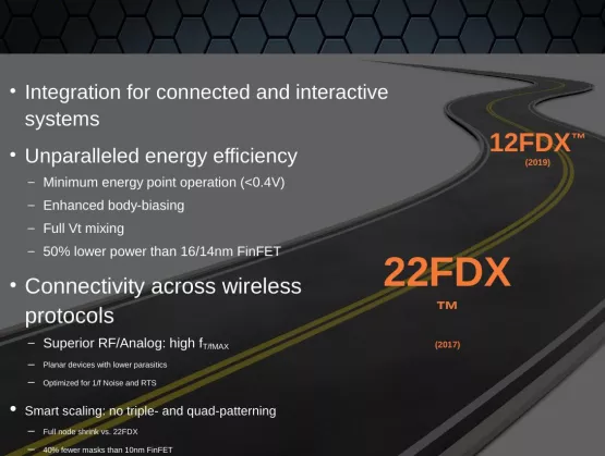
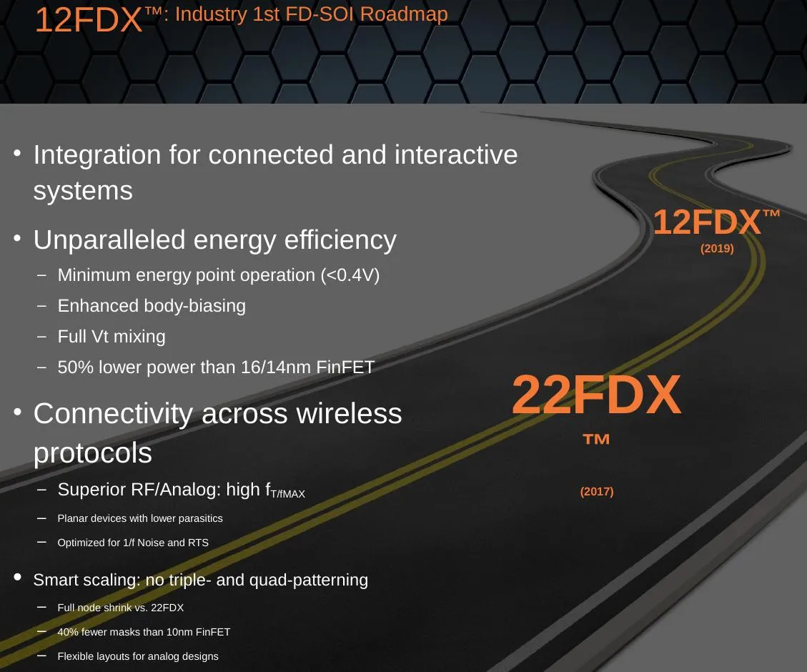
12nm FD-SOI has now officially joined the GlobalFoundries’ roadmap, targeting intelligent, connected systems and beating 14/16nm FinFET on performance, power consumption (by 50%!) and cost (see press release here). Customer product tape-outs are expected to begin in the first half of 2019. GloFo also announced FDXcelerator™, an ecosystem designed to give 22FDX™ SoC design a boost and reduce time-to-market for its customers (press release here). [caption id="attachment_9874" align="aligncenter" width="610"] (Courtesy: GlobalFoundries and SOI Consortium Shanghai FD-SOI Forum 2016)[/caption] The news turned heads worldwide (hundreds of publications immediately picked up the news) – and especially in China. "We are excited about the GlobalFoundries 12FDX offering and the value it can provide to customers in China," said Dr. Xi Wang, Director General, Academician of Chinese Academy of Sciences, Shanghai Institute of Microsystem and Information Technology. “Extending the FD-SOI roadmap will enable customers in markets such as mobile, IoT, and automotive to leverage the power efficiency and performance benefits of the FDX technologies to create competitive products." Wayne Dai, CEO of VeriSilicon (headquartered in Shanghai but designing for the world’s biggest names in the chip biz), added, “We look forward to extending our collaboration with GlobalFoundries on their 12FDX offering and providing high-quality, low-power and cost-effective solutions to our customers for the China market. The unique benefits of FD-SOI technologies enable us to differentiate in the automotive, IoT, mobility, and consumer market segments.” The ultra-thin FD-SOI wafers are where it all starts, and they’re ready to go in high volume, says Paul Boudre, CEO of SOI wafer leader Soitec. “We are very pleased to see a strong momentum and a very solid adoption from fabless customers in 22FDX offering,” he adds. “Now this new 12FDX offering will further expand FD-SOI market adoption. This is an amazing opportunity for our industry just in time to support a big wave of new mobile and connected applications.” All About 12GloFo’s 12FDXTM platform, which builds on the success of its 22FDXTM offering, is designed to enable the intelligent systems of tomorrow across a range of applications, from mobile computing and 5G connectivity to artificial intelligence and autonomous vehicles. Increased integration of intelligent components including wireless (RF) connectivity, non-volatile memory, and power management—all while driving ultra-low power consumption—are key 12FDX selling points that FinFETs can’t touch. The technology also provides the industry’s widest range of dynamic voltage scaling and unmatched design flexibility via software-controlled transistors—capable of delivering peak performance when and where it is needed, while balancing static and dynamic power for the ultimate in energy efficiency. [caption id="attachment_9873" align="aligncenter" width="610"] (Courtesy: GlobalFoundries and SOI Consortium Shanghai FD-SOI Forum 2016)[/caption] “Some applications require the unsurpassed performance of FinFET transistors, but the vast majority of connected devices need high levels of integration and more flexibility for performance and power consumption, at costs FinFET cannot achieve,” said GLOBALFOUNDRIES CEO Sanjay Jha. “Our 22FDX and 12FDX technologies fill a gap in the industry’s roadmap by providing an alternative path for the next generation of connected intelligent systems. And with our FDX platforms, the cost of design is significantly lower, reopening the door for advanced node migration and spurring increased innovation across the ecosystem.” Kudos came in from G. Dan Hutcheson, CEO of VLSI Research, IBS CEO Handel Jones, Linley Group Founder Linley Gwennap, Dasaradha Gude, CEO of IP/design specialists INVECAS, Leti CEO Marie Semeria and NXP VP Ron Martino (they’ve already started on 28nm FD-SOI for their i.MX line – read his superb explanations in ASN here). 22 Design Plug ‘n PlaySimultaneously to the 12FDX announcement, GloFo announced the FDXcelerator Partner Program. It creates an open framework under which selected Partners can integrate their products or services into a validated, plug and play catalog of design solutions. This level of integration allows customers to create high performance designs while minimizing development costs through access to a broad set of quality offerings, specific to 22FDX technology. The Partner ecosystem positions members and customers to take advantage of the broad adoption and accelerating growth of the FDX market.Initial partners of the FDXcelerator Partner Program are: Synopsys (EDA), Cadence (EDA), INVECAS (IP and Design Solutions), VeriSilicon (ASIC), CEA Leti (services), Dreamchip (reference solutions) and Encore Semi (services). These companies have already initiated work to deliver advanced 22FDX SoC solutions and services. Initial FDXcelerator Partners have committed a set of key offerings to the program, including: tools (EDA) that complement industry leading design flows by adding specific modules to easily leverage FDSOI body-bias differentiated features, a comprehensive library of design elements (IP), including foundation IP, interfaces and complex IP to enable foundry customers to start their designs from validated IP elements, platforms (ASIC), which allow a customer to build a complete ASIC offering on 22FDX, reference solutions (reference designs, system IP), whereby the Partner brings system level expertise in Emerging application areas, enabling customers to speed-up time to market, resources (design consultation, services), whereby Partners have trained dedicated resources to support 22FDX technology; and product packaging and test (OSAT) solutions. Additional FDXcelerator members will be announced in the following months.
Read More