downloadGroupGroupnoun_press release_995423_000000 copyGroupnoun_Feed_96767_000000Group 19noun_pictures_1817522_000000Member company iconResource item iconStore item iconGroup 19Group 19noun_Photo_2085192_000000 Copynoun_presentation_2096081_000000Group 19Group Copy 7noun_webinar_692730_000000Path
Skip to main content
Default Banner Image

RF

“GlobalFoundries, TowerJazz, TSMC and UMC are expanding or bringing up RF SOI processes in 300mm fabs in an apparent race to garner the first wave of RF business for 5G, the next-generation wireless standard,” writes Mark Lapedus of Semiconductor Engineering. His recent piece, RF-SOI Wars Begin, explains why demand across the supply chain is currently tight. Rest assured, the supply situation is being addressed fast. By next year, 300mm-based RF-SOI manufacturing (vs. 200mm) will increase from 5% to 20%. But with insatiable end-user demand for greater throughput, overall RF-SOI device demand is increasing in the double-digit range, so 200mm-based manufacturing is also expanding fast. [caption id="attachment_11905" align="alignleft" width="300"] The front-end modules in all smartphones are built on Soitec's RF-SOI wafer technology. The most advanced, for LTE/LTE-A, are built on Soitec's RFeSI-SOI wafers, which have four layers to meet the demands of devices with high linearity requirements. (Courtesy: Soitec)[/caption] SOI wafer manufacturer Soitec has 70% of the RF-SOI wafer market share. The other RF-SOI wafer manufacturers – Shin-Etsu, GlobalWafers and Simgui – all use Soitec's RF-SOI wafer manufacturing technology. This is an excellent, comprehensive piece, that clearly explains the complexities of the markets, the devices, the manufacturing and the supply chain. It's a highly recommended read. BTW, the SOI Consortium is organizing a 4G/5G SOI supply chain workshop during Semicon West (July '18). Sign up or get more information on that under the Events tab here on the consortium website. Of course, here at ASN, we've been covering RF-SOI for over a decade. You can use our RF-SOI tag to access most of the pieces we've done over the years.
Read More
Good news: there are far fewer bigoted extremists out there when it comes to FD-SOI vs. FinFETs. People want the best technology for their application. It's that simple. That's a key piece of news from the updated survey by Dan Hutcheson, CEO of VLSI Research, which he presented in the afternoon session of the SOI Consortium's 2018 SOI Symposium in Silicon Valley The afternoon then featured presentations by foundry partners, which I'll cover here. Also in the afternoon were presentations by wafer-maker Simgui, some innovative start-ups leveraging FD-SOI for custom SoCs and the final panel discussion. I'll cover those in Part 3 of this series. BTW, if somehow you missed my coverage of the morning sessions about very cool new products and projects from NXP, Sony, Audi, Airbus and Andes Technology, be sure to click here to read it. The presentations are starting to be posted on the SOI Consortium Events page – but some won't be. Either way, I'll cover them here. VLSI Research A couple years ago at the annual SOI Symposium in Silicon Valley, Dan Hutcheson presented results of a survey he did (ASN covered it – you can still read about it here). At the 2018 event, he presented an update, which is now posted. You can get it here. The FD-SOI roadmap and IP availability are no longer issues for decision makers, he found. The 14nm branch – do you go FinFET or FD-SOI? – is gone. “Fins and FD are complementary,” he observed. Most people said they'd consider using both and running two roadmaps, choosing whichever technology is appropriate to a given design. [caption id="attachment_11841" align="alignnone" width="1000"] (Courtesy: VLSI Research, SOI Consortium)[/caption] From a transistor viewpoint, the top reasons to choose FD-SOI is that it's better for analog and has lower leakage/parastics. It's perceived as better for complex, high mixed-signal SoCs, and especially for RF and sensor integration. In fact, people see RF as the new mixed-signal, wherein FD-SOI is uniquely positioned for 5G and mmWave. From a business viewpoint, FD-SOI is perceived to have real advantages. In particular, FD-SOI wins when it comes to keeping down design costs, manufacturing costs and time-to-market. IoT is still the hottest target market for FD-SOI, to which he adds high growth expected in automotive and medical. Samsung With 20 tape-outs in 2018, Samsung is seeing an acceleration in its FD-SOI business. “The trend is healthy,” said Hong Hoa, SVP of the company's foundry business. FD-SOI, he continued, is on a “differentiation path.” Samsung's 28nm FD-SOI process, called 28FDS is at full maturity with very strong yields. They're seeing more customers and a wider range of applications. The design infrastructure, silicon-verified IP and methodologies are also all mature. They have optimal implementation and verification guidelines for body bias design, a body bias memory usage guide, and a body bias generator integration guide. The process supports Grade 1 automotive, and will be qualified for Grade 2 in a few weeks. FD-SOI, Hoa reminded the audience, offers superior RF performance compared to both planar bulk and 14nm FinFET. The Samsung strategy is to first provide a base for for the FD-SOI process, then add RF and eMRAM. The base for 28nm was done in 2016; they added RF in 2017 and eMRAM this year. The Samsung platform for IoT applications integrates both RF and eMRAM to support multi-function needs in a single platform. Lead customers are already working with eMRAM in their designs, he added. (BTW, Samsung has a really nice video explaining their eMRAM offering – you can see it on YouTube here.) The basic PDK for the Samsung 18nm FD-SOI process (18FDS) will be available in September 2018, with full production slated for fall of 2019. It will deliver a 24% increase in performance, a 38% decrease in power, and a 35% decrease in area for logic. RF for the 18FDSplatform will be ready by the end of this year, and eMRAM beginning in 2019. GlobalFoundries With design wins from 36 customers underway, 12 of which are taping out in 22FDX (GF's 22nm FD-SOI process) this year, the market has validated FDX for differentiation, said GF SVP Dr. Bami Bastani. And indeed, designers are using it for a wide array of applications across North America, Europe, Asia/Pacific and Japan. Customers in the North America are designing in 22FDX for NB-IoT, industrial, RF/analog, mobile, network switches and cryptocurrency applications. In Europe, it's more or less the same plus automotive/mmWave, optical transmission, wireless BTS and AI/ML. In Asia Pacific/Japan the mix is similar to Europe. Bastani sees the three big enablers as the the strengths of the roadmap, the ecosystem and multi-sourcing from Dresden and Chengdu (where they're already equipping the cleanrooms). He also tipped his hat in acknowledgment to the partnership with FD-SOI wafer supplier Soitec, noting that they have gone the extra mile to match GF's requirements. So that was the first part of a great afternoon. As mentioned above, my next post (part 3) will cover a very informative presentation by wafer-maker Simgui on the markets in China, plus talks by some innovative start-ups leveraging FD-SOI for custom SoCs and the final panel discussion.
Read More
GlobalFoundries' new ecosystem partner program, called RFwave™, aims to simplify RF design and help customers reduce time-to-market for a new era of wireless devices and networks (read the full press release here). The program aims to give designers a low-risk, cost-effective path to highly optimized solutions that leverage GF's platforms including RF on FD-SOI and RF-SOI. The target is wireless applications such as IoT across various wireless connectivity and cellular standards, standalone or transceiver integrated 5G front end modules, mmWave backhaul, automotive radar, small cell and fixed wireless and satellite broadband. As such, the RFwave™ partner program provides GF customers with IP design elements, EDA tools, design consultation and services and OSAT product packaging and test solutions. These products and services are validated, and comprise a plug-and-play catalog of design solutions. With this level of integration, GF customers can create high-performance designs while minimizing development costs. Bami Bastani, senior vice president of GF’S RF Business Unit, says, “As a leader in RF, GF’s RFwave program takes industry collaboration to a new level, enabling our customers to build differentiated, highly integrated RF-tailored solutions that are designed to accelerate the next wave of technology.” Initial members of the RFwave Partner Program are: asicNorth, Cadence, CoreHW, CWS, Keysight Technologies, Spectral Design, and WEASIC.
Read More
Following the immense success of last year's FD-SOI training day in Silicon Valley, the SOI Consortium has another one planned for the end of April this year. If you want to start learning how to leverage FD-SOI in your chip designs, this is a great place to start. Click here for information on how to sign up. ST Fellow Dr. Andreia Cathelin has put together another great line-up. World renowned professors and experts from industry will deliver a series of four training sections of 1.5 hours each, focused on energy efficient and low-power, low-voltage design techniques for analog, RF, high-speed, mmW and mixed-signal design. You'll learn about design techniques that take full advantage of the unique features of FD-SOI, including body biasing capabilities that further enhance the excellent analog/RF performances of these devices. Each section of this training day will take you through concrete design examples that illustrate new implementation techniques enabled by FD-SOI technologies at the 28nm and 22nm nodes – and beyond. The design examples will cover basic building blocks through SoC implementations. A global Q A session will close the day. Here's a little more info on how the day will unfold. Click on the slides to see them in full screen. Morning sessionsFDSOI-specific design techniques for analog, RF and mmW applications - Andreia Cathelin, Fellow, STMicroelectronics [caption id="attachment_11714" align="alignleft" width="300"] Quick preview from Andreia Cathelin's FD-SOI training session (Courtesy: STMicroelectronics, SOI Consortium)[/caption] Andreia Cathelin is ST's key design scientist for all advanced CMOS technologies, and is arguably the world's leading expert on leveraging FD-SOI in high-performance, low-power RF/AMS SoCs. Her course will first present a very short overview of the major analog and RF technology features of 28nm FDSOI technology. Then the focus moves to the benefits of FD-SOI technology for analog/RF and millimeter-wave circuits. She'll give design examples such as analog low-pass filters, inverter-based analog amplifiers and 30GHz and 60GHz Power Amplifiers, as well as mmW oscillators. There will be particular focus on the advantages of body biasing and special design techniques offering state-of-the-art performance. Circuit Design Techniques in 22nm FD-SOI for 5G 28GHz Applications - Frank Zhang, Principal Member of Technical Staff, GlobalFoundries [caption id="attachment_11716" align="alignright" width="300"] Quick preview from Frank Zhang's FD-SOI training session (Courtesy: GlobalFoundries, SOI Consortium)[/caption] Frank Zhang has designed chips using GF's 22nm FD-SOI (22FDX) process for WLAN, 5G cellular and automotive radar applications. His course will focus on how to take advantages of FD-SOI’s high-frequency performance at relatively low-current density to design high performance RF/mmWave circuits. Examples circuits include a 28GHz LNA, a 28GHz PA and an RF switch for 5G applications. The FD-SOI advantages such as low capacitance, high breakdown voltage and high-output impedance will be exploited in these design examples. This course will also discuss how to extend these techniques to applications at higher frequencies and/or higher current densities that are subject to extreme temperatures and EM requirements. Afternoon sessionsEnergy-Efficient Design in FDSOI - Bora Nikolic, Professor, UC Berkeley [caption id="attachment_11715" align="alignleft" width="300"] Quick preview from Bora Nikolić's FD-SOI training session (Courtesy: UC Berkeley, SOI Consortium)[/caption] Borivoje (“Bora”) Nikolić is known as one of the world’s top experts in body-biasing for digital logic (he and his team have designed more than ten chips in ST’s 28nm FD-SOI.) If you missed it, his team's RISC-V chip was cited as one of Dr. Cathelin's “Outstanding 28nm FD-SOI Chips Taped Out Through CMP” – read more about that here. His talk at the training day will present options for energy-efficient mixed-signal and digital design in FD-SOI technologies. He'll explain how to generate body bias and use it to improve efficiency, with examples in RF and baseband building blocks, temperature sensors, data converters and voltage regulators. The techniques will be presented in the context of UC Berkeley's latest RISC-V-based SoC, designed to operate in a very wide voltage range using 28nm FD-SOI. mm-Wave and Fiber-Optics Design in FD-SOI CMOS Technologies - Sorin Voinigescu, Professor, University of Toronto [caption id="attachment_11713" align="alignright" width="300"] Quick preview from Sorin Voinigescu's FD-SOI training session (Courtesy: U. Toronto, SOI Consortium)[/caption] Sorin Voinigescu is a world renowned expert on millimeter-wave and 100+Gb/s ICs and atomic-scale semiconductor device technologies. His lecture will cover the main features of FD-SOI CMOS technology and how to efficiently use its unique features and suitable circuit topologies for mm-wave and broadband SoCs. He'll begin with an overview of the impact of the back-gate bias and temperature on the measured I-V, transconductance, fT, and fMAX characteristics. Then he'll compare the maximum available gain, MAG, of FDSOI MOSFETs with those of planar bulk CMOS and SiGe BiCMOS transistors through measurements up to 325 GHz. Next, he'll provide biasing, sizing and step-by-step design examples for VCO, doubler, switches, PA, large swing optical modulator drivers and quasi-CML circuit topologies and layouts that make efficient use of the back-gate bias to overcome the limitations associated with the low breakdown voltage of 20nm and 12nm FD-SOI CMOS technologies. Sign Up Now!With over 100 attendees filling every chair in the auditorium, last year's training day was sold out. Although it was in Silicon Valley, people actually flew in from all over the world to be there. During the Q A at the end, most everyone prefaced their questions by saying, “Thank you. I really learned a lot today.” 2018 will be no different – except that it's sure to sell out even faster. Please note, though, that this is not a free event, so only the attendees will get copies of the slide decks. Here's key info you need to sign up. See you there!What: SOI Consortium's FD-SOI Training DayWhen: 27 April 2018, 7:30am – 5pm.Where: Crowne Plaza San Jose, Milpitas CA (parking is free)Registration fee: US $485.00 (includes training book, breakfast, box lunch and refreshments during breaks)How to sign up: Click here to go directly to the registration site.
Read More
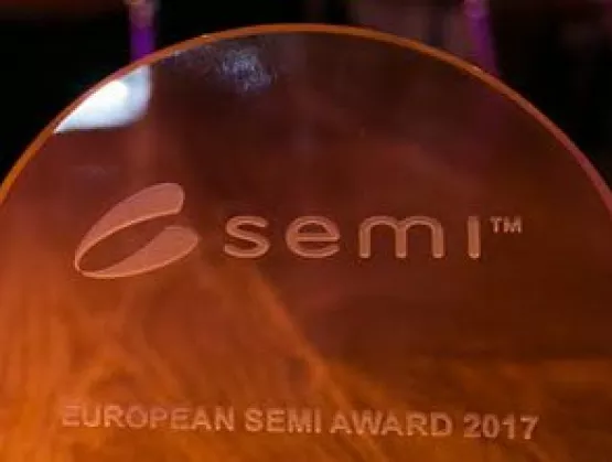
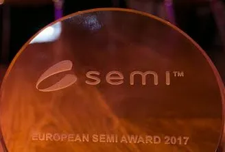
RF-SOI innovators Jean-Pierre Raskin of UCL and Bernard Aspar of Soitec changed the course for key RF chips. The industry has long recognized their contributions: their solution for “trap-rich” RF-SOI wafers is now the starting point to virtually every FEM in every smart phone on the planet (really!). And of course here at ASN we've been following their work for over a decade. Now more accolades are coming in. The latest is the 2017 European SEMI Award, which was given at ISS Europe 2018 for “...their seminal work with radio frequency silicon-on-insulator (RF-SOI) substrates” (read the press release here). As SEMI notes, the “...award winners’ pioneering research and collaboration with academia and industry led to major advances in RF switches and ushered RF-SOI technology from concept to worldwide adoption.” Aspar and Raskin were nominated and selected by their peers within the international semiconductor community. [caption id="attachment_11677" align="alignleft" width="150"] Bernard Aspar, Executive Vice President, Communication Power BU at Soitec Aspar founded CEA-Leti spinoff Tracit Technologies in 2003. He was appointed senior vice president of the Tracit Division (now the Communication Power business unit) when Soitec acquired Tracit in 2006. He has more than 15 years of experience in direct wafer-bonding and layer transfer. Aspar has filed more than 35 patents and co-authored some 100 scientific articles. He holds engineering and Ph.D. degrees in materials sciences and a master’s degree in microelectronics from the University of Montpellier, France.[/caption] [caption id="attachment_11678" align="alignleft" width="150"] Jean-Pierre Raskin, professor, Université catholique de Louvain (UCL) Raskin contributed to pioneering scientific studies demonstrating that silicon-based MOS technology could enable affordable, high-quality mobile devices. His findings led to the advent of RF-SOI technology and today impact the global microelectronics industry. He is an IEEE Senior Member, EuMA Associate Member and Member of the Research Center in Micro and Nanoscopic Materials and Electronic Devices of the Université catholique de Louvain, where he has been a full professor since 2007. He is author or co-author of more than 350 scientific articles.[/caption] Their advanced RF-SOI technology is now behind a wide range of applications and systems in areas including mobile devices, satellite communications, IoT, automotive radar and aerospace. If you want to better understand all this, a few years ago UCL and Soitec teams contributed an excellent article to ASN. It clearly explains how and why these new substrates came to be. You can still read it here. (Or if you're still a little confused about RF-SOI vs. RF on FD-SOI, here's a piece we did back in 2015 that explains the basics.)
Read More
Big News: Samsung has officially revealed that their next FD-SOI node is 18nm. The announcement was made at the recent Samsung Foundry Forum, which showcased a number of new technologies that the company says will help enable the development of new devices connecting consumers in entirely new ways. (You can read the full press release here.) Samsung also announced new features for its 28nm FD-SOI offering, which is called 28FDS. Noting that it is well suited for IoT applications, Samsung said it will gradually expand its 28FDS technology into a broader platform offering by incorporating RF and eMRAM(embedded Magnetic RAM) options. 18FDS is the next generation node on Samsung’s FD-SOI roadmap with enhanced PPA (Power/Performance/Area). [caption id="attachment_10762" align="alignnone" width="705"] Kinam Kim, President of Samsung Electronics’ Semiconductor Business, introduces the company’s newest foundry process technologies and solutions. (Courtesy: Samsung)[/caption] The FD-SOI news was part of an announcement covering Samsung's newest process technology roadmap. “The ubiquitous nature of smart, connected machines and everyday consumer devices signals the beginning of the next industrial revolution,” said Jong Shik Yoon, Executive Vice President of the Foundry Business at Samsung Electronics. “To successfully compete in today’s fast-paced business environment, our customers need a foundry partner with a comprehensive roadmap at the advanced process nodes to achieve their business goals and objectives.”
Read More
They're calling it, “The most advanced, lowest power-consuming GPU-enabled MPU on the market.” It's NXP's new i.MX 7ULP general-purpose processor, and it's on 28nm FD-SOI. They've got a nifty video summing it all up – you can watch it here. [caption id="attachment_10388" align="alignleft" width="300"] NXP is first to market with a general-purpose processor on FD-SOI: the i.MX 7ULP. It's got both ultra-low power consumption and rich graphics for battery powered applications. (Courtesy: NXP)[/caption] With the i.MX 7ULP, NXP is first to market with an FD-SOI applications processor offering the industry’s lowest power consumption. The debut was made at the recent Embedded World Conference in Nuremberg, Germany, and it made a big splash in media across the globe. (Read the full press release here.) In deep sleep mode, it boasts power consumption of just 15 uW or less: 17 times less than previous (and highly successful) low power i.MX 7 devices. Dynamic power efficiency is improved by 50 percent on the real-time domain.The i.MX 7ULP applications processor family is currently sampling to select customers. Broader availability of pre-production samples is scheduled for Q3 2017.Hello, IoT!The high-performance, low-power solution is optimized for customers developing applications that spend a significant amount of time in standby mode with short bursts of performance-intense activity that require exceptional graphics processing. Sounds like IoT – and indeed it is, and more.With the i.MX 7ULP, NXP's targeting wearables, portable healthcare, smart home controls, gaming accessories, building automation, general embedded control and IoT edge solutions. Bottom line: it's designed to enable ultra-low-power and secure, portable applications – especially those demanding long battery life. (Read the current fact sheet here.)The detailsThe i.MX 7ULP features an advanced implementation of the ARM® Cortex®-A7 core, the ARM Cortex-M4 core, as well as a 3D and 2D Graphic Processing Units (GPUs). It's got a 32-bit LPDDR2/LPDDR3 memory interface and a number of other interfaces for connecting peripherals, such as WLAN, Bluetooth, GPS, displays, and camera sensors. [caption id="attachment_10387" align="alignnone" width="834"] (Courtesy: NXP)[/caption] NXP says this new design, based on FD-SOI’s lower voltage capability, enables rich user experience through extremely power-efficient graphics acceleration, a fundamental requirement in many of today’s consumer and industrial battery-operated devices that incorporate robust graphic interfaces. Further enablement includes rich Linux or Android ecosystem with the real-time capability supported by FreeRTOS.Leveraging body biasing and moreNXP credits the design’s extreme low leakage and operating voltage (Vdd) scalability to that FD-SOI specialty: reverse and forward body biasing (RBB/FBB) of the transistors, and its smart power system architecture.In presenting the new i.MX 7ULP to the tech press, the company highlighted the following FD-SOI design advantages: Large dynamic gate and body biasing voltage range Domain and subsystem optimization with custom standard cell library with mixed voltages Low quiescent current (Iq) bias generators Enhanced ADC performance with unique FD-SOI attributes Fail Safe I/O for simplified low power system design To that, add a note about security. As the chip's fact sheet says, “The processors deliver hardware-enabled security features that enable secure e-commerce, digital rights management (DRM), information encryption secure boot, and tamper detection.” Those are just the sort of things that demand the bursts of high performance that dynamic forward body biasing delivers where and when it's needed.Samsung fabs, Verisilicon adds IPTwo other SOI Consortium members – Samsung and Verisilicon – are particularly pleased with NXP's results.“We are excited that NXP is the first to bring the benefits of FD-SOI (28FDS) technology to the general purpose market,” says Ryan Lee, VP of the Foundry Marketing Team at Samsung Electronics. “28FDS technology will satisfy a growing and critical need for ultra low power designs that require power-performance at very low voltages. We plan to evolve 28FDS technology to a differentiated low-power single platform by implementing RF and embedded Non-Volatile Memory (eNVM) solution for our customers’ success.”NXP’s processor design enables robust low power graphics for the IoT and wearable markets through two graphic processor units (GPU) from Vivante: the GC7000 NanoUltra 3D GPU with a low power single shader, and the GC320 Composition Processing Core (CPC) for 2D graphics. The 3D GPU plays a critical role in enabling rich 3D based user interfaces, while the CPC can accelerate both rich 3D and simpler 2D user interfaces. Processors based on the combination of the two GPUs enable efficient display systems which offload and significantly reduce system resources, in turn providing rich user interfaces at low power levels to extend the battery life of devices.“Our 3D GPU is a result of a joint collaboration between Vivante and NXP to deliver industry-leading 3D capabilities with the lowest power consumption,” said Wei-Jin Dai CEO at Vivante Corporation and Chief Strategy Officer and GM of the IP Division at Verisilicon. “The power savings from using the right GPU in an ultra low power processor is one of the major attributes and advantages of the architecture.”So, now shall we dig in a little deeper into the “why FD-SOI” question? Read on in Part 2 of this article.-- By Adele Hars, ASN Editor-in-Chief
Read More
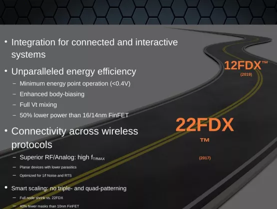
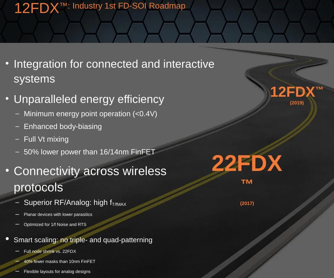
12nm FD-SOI has now officially joined the GlobalFoundries’ roadmap, targeting intelligent, connected systems and beating 14/16nm FinFET on performance, power consumption (by 50%!) and cost (see press release here). Customer product tape-outs are expected to begin in the first half of 2019. GloFo also announced FDXcelerator™, an ecosystem designed to give 22FDX™ SoC design a boost and reduce time-to-market for its customers (press release here). [caption id="attachment_9874" align="aligncenter" width="610"] (Courtesy: GlobalFoundries and SOI Consortium Shanghai FD-SOI Forum 2016)[/caption] The news turned heads worldwide (hundreds of publications immediately picked up the news) – and especially in China. "We are excited about the GlobalFoundries 12FDX offering and the value it can provide to customers in China," said Dr. Xi Wang, Director General, Academician of Chinese Academy of Sciences, Shanghai Institute of Microsystem and Information Technology. “Extending the FD-SOI roadmap will enable customers in markets such as mobile, IoT, and automotive to leverage the power efficiency and performance benefits of the FDX technologies to create competitive products." Wayne Dai, CEO of VeriSilicon (headquartered in Shanghai but designing for the world’s biggest names in the chip biz), added, “We look forward to extending our collaboration with GlobalFoundries on their 12FDX offering and providing high-quality, low-power and cost-effective solutions to our customers for the China market. The unique benefits of FD-SOI technologies enable us to differentiate in the automotive, IoT, mobility, and consumer market segments.” The ultra-thin FD-SOI wafers are where it all starts, and they’re ready to go in high volume, says Paul Boudre, CEO of SOI wafer leader Soitec. “We are very pleased to see a strong momentum and a very solid adoption from fabless customers in 22FDX offering,” he adds. “Now this new 12FDX offering will further expand FD-SOI market adoption. This is an amazing opportunity for our industry just in time to support a big wave of new mobile and connected applications.” All About 12GloFo’s 12FDXTM platform, which builds on the success of its 22FDXTM offering, is designed to enable the intelligent systems of tomorrow across a range of applications, from mobile computing and 5G connectivity to artificial intelligence and autonomous vehicles. Increased integration of intelligent components including wireless (RF) connectivity, non-volatile memory, and power management—all while driving ultra-low power consumption—are key 12FDX selling points that FinFETs can’t touch. The technology also provides the industry’s widest range of dynamic voltage scaling and unmatched design flexibility via software-controlled transistors—capable of delivering peak performance when and where it is needed, while balancing static and dynamic power for the ultimate in energy efficiency. [caption id="attachment_9873" align="aligncenter" width="610"] (Courtesy: GlobalFoundries and SOI Consortium Shanghai FD-SOI Forum 2016)[/caption] “Some applications require the unsurpassed performance of FinFET transistors, but the vast majority of connected devices need high levels of integration and more flexibility for performance and power consumption, at costs FinFET cannot achieve,” said GLOBALFOUNDRIES CEO Sanjay Jha. “Our 22FDX and 12FDX technologies fill a gap in the industry’s roadmap by providing an alternative path for the next generation of connected intelligent systems. And with our FDX platforms, the cost of design is significantly lower, reopening the door for advanced node migration and spurring increased innovation across the ecosystem.” Kudos came in from G. Dan Hutcheson, CEO of VLSI Research, IBS CEO Handel Jones, Linley Group Founder Linley Gwennap, Dasaradha Gude, CEO of IP/design specialists INVECAS, Leti CEO Marie Semeria and NXP VP Ron Martino (they’ve already started on 28nm FD-SOI for their i.MX line – read his superb explanations in ASN here). 22 Design Plug ‘n PlaySimultaneously to the 12FDX announcement, GloFo announced the FDXcelerator Partner Program. It creates an open framework under which selected Partners can integrate their products or services into a validated, plug and play catalog of design solutions. This level of integration allows customers to create high performance designs while minimizing development costs through access to a broad set of quality offerings, specific to 22FDX technology. The Partner ecosystem positions members and customers to take advantage of the broad adoption and accelerating growth of the FDX market.Initial partners of the FDXcelerator Partner Program are: Synopsys (EDA), Cadence (EDA), INVECAS (IP and Design Solutions), VeriSilicon (ASIC), CEA Leti (services), Dreamchip (reference solutions) and Encore Semi (services). These companies have already initiated work to deliver advanced 22FDX SoC solutions and services. Initial FDXcelerator Partners have committed a set of key offerings to the program, including: tools (EDA) that complement industry leading design flows by adding specific modules to easily leverage FDSOI body-bias differentiated features, a comprehensive library of design elements (IP), including foundation IP, interfaces and complex IP to enable foundry customers to start their designs from validated IP elements, platforms (ASIC), which allow a customer to build a complete ASIC offering on 22FDX, reference solutions (reference designs, system IP), whereby the Partner brings system level expertise in Emerging application areas, enabling customers to speed-up time to market, resources (design consultation, services), whereby Partners have trained dedicated resources to support 22FDX technology; and product packaging and test (OSAT) solutions. Additional FDXcelerator members will be announced in the following months.
Read More
By: Tamer Ragheb,Digital Design Methodology Technical Manager at GlobalFoundries and Josefina Hobbs, Senior Manager of Strategic Alliances, Synopsys It’s clear that getting an optimal balance of power and performance at the right cost is foremost in the minds of designers today. Designers who want either high performance or ultra low-power, or ideally both, have a choice to make when it comes to migrating to next generation nodes. For applications that push the envelope in performance, FinFET would be the optimal solution. For applications that require ultra low-power and more RF integration, FD-SOI is the right solution. The two technologies have different value propositions that need to be considered while designing for applications ranging from high-performance computing and server to high-end mobile and Internet of Things (IoT). GlobalFoundries 22FDX is the industry’s very first 22nm FD-SOI platform. The 22FDX technology is specifically designed to meet the ultra low-power requirements of the next generation of connected devices. The big advantage of this platform is its ability to provide software control at the transistor level through flexible body-biasing (Fig. 1). The ability to provide real-time trade-offs between power and performance via software-controlled body-biasing of the transistor creates new options for the designer. For example, imagine designing a processor for a Smartwatch that could match its power-performance tradeoff to your typical use and modify its performance based on how you’re using it that day. [caption id="attachment_9473" align="alignleft" width="610"] Figure 1: Benefits of 22FDX body-biasing[/caption] The full impact of the body bias capability of 22FDX becomes clear when compared to incumbent high-performance process technologies (Fig. 2). 22FDX compared to a 28nm high K metal gate (HKMG) technology can provide up to 50% less power at the same frequency, or 40% faster performance at the same total power than 28HKMG. In addition, 22FDX can be further optimized with forward body bias, shown on the blue curve, to further reduce the power or to further boost the speed in a turbo operation mode. [caption id="attachment_9474" align="alignleft" width="610"] Figure 2: 22FDX Body Bias Optimizes Performance and Power[/caption] In addition to the body bias, 22FDX offers capabilities for design flexibility and intelligent control that are not available in other technologies. These include: Improved electrostatic control of the transistor acts as a performance booster and enables lower VDD (i.e., lower power consumption) while reaching significant performance Low variability and body-biasing capability that can achieve 0.4 volt operation Complete RF enablement with ‘knobs’ to reduce RF power by up to 50 percent Manufacturing success is highly sensitive to specific physical design features, with advanced nodes requiring more complex design rules and more attention to manufacturability issues on the part of designers. However, there are essentially no additional manufacturing requirements to design in 22FDX beyond what is required for 28nm designs. There are four application optimized extensions available with 22FDX (Fig. 3). These are: 22FDX ULP- an ultra low-power extension that provides logic libraries and memory compilers that are optimized for 0.4 volt operation. 22 FDX ULL- an ultra low-leakage extension that brings in an expanded device suite capable of achieving one pico-amp per micron leakage. 22 FDX UHP- an ultra high-performance extension that leverages the overdrive capabilities and body-biasing features to maximize the performance of technologies in a turbo or a burst mode. It has high performance libraries and high speed interfaces and BEOL stacks optimized for competing architectures or applications. 22 FDX RFA- an RF and analog extension that brings in full characterization and enablement for RF applications, including optimized RF layouts and P cells, BEOL passives, and IP for Bluetooth LE and WIFI applications. [caption id="attachment_9475" align="alignleft" width="610"] Figure 3: 22FDX Platform and Extensions[/caption] GlobalFoundries reference flow for 22FDX has been optimized to support forward and reverse body bias (FBB/RBB), which provides the design flexibility to optimize the performance/power trade-offs. The reference flow supports implant-aware and continuous diffusion-aware placement, tap insertion and body bias network connectivity according to high voltage rules, double-patterning aware parasitic extraction (PEX), and design for manufacturing (DFM). This provides designers with the flexibility to manage power, performance and leakage targets for the next-generation chips used in mainstream mobile, IoT and networking applications. GlobalFoundries has been collaborating with Synopsys to enable and qualify their tools for the 22FDX Reference Flow. The recent qualification of Synopsys’ Galaxy™ Design Platform for the current version ofGlobalFoundries’ 22FDX technology allows the designer to manage power, performance and leakage and achieve optimal energy efficiency and cost effectiveness. Synopsys’ Galaxy Design Platform supports body biasing techniques throughout the design flow, including both forward and reverse body bias, enabling power/performance trade-offs to be made dynamically and delivering up to 50% power reduction. Key tools and features of the Galaxy Design Platform in the 22FDX reference flow include: Design Compiler® Graphical synthesis with IEEE 1801 (UPF) driven bias-aware multi-corner multi-mode (MCMM) optimization Formality® formal verification with bias-aware equivalence checking IC Compiler™ and IC Compiler II™ layout with physical implementation support for non-uniform library floorplanning, implant-aware placement, multi-rail routing, and advanced power mesh creation StarRC™ parasitic extraction for multi-rail signoff with support for multi-valued standard parasitic exchange format (SPEF) PrimeTime® timing analysis and signoff including distributed multi-scenario analysis (DMSA) static timing and noise analysis, using AOCV and POCV technology IC Validator In-Design physical verification The 22FDX technology leverages existing design tools such as the Galaxy Design Platform, manufacturing infrastructure and the broader design ecosystem. This speeds time to market and enables the creation of differentiated products.
Read More