downloadGroupGroupnoun_press release_995423_000000 copyGroupnoun_Feed_96767_000000Group 19noun_pictures_1817522_000000Member company iconResource item iconStore item iconGroup 19Group 19noun_Photo_2085192_000000 Copynoun_presentation_2096081_000000Group 19Group Copy 7noun_webinar_692730_000000Path
Skip to main content
Default Banner Image

SEMI Japan

In an important step toward resuming business as usual in Japan, Prime Minister Shinzo Abe on May 14 lifted the state of emergency originally scheduled to expire at the end of May for 39 of Japan’s 47 prefectures, marking “the real beginning of our efforts toward a new normal in the era of the coronavirus” as new cases continue to decline. But with Tokyo, Osaka and six other prefectures still under the state of emergency, Abe urged citizens to remain cautious as the nation and world continue to confront the COVID-19 threat. Among criteria the remaining prefectures must meet for a state of emergency suspension is a reduction in new infections to no more than 0.5 cases weekly for every 100,000 citizens. The eight prefectures account for nearly half of Japan’s population and GDP, with Tokyo and Osaka the two largest urban areas in the island nation. Japan expects to contain its economic losses to 38 trillion yen, 15 percent less than the 45 trillion yen hit originally projected. The Japan government has planned a May 21 progress review[1] in the eight prefectures, a timeline that Abe said could lead to the lifting of the state of emergency before the original cutoff at the end of the month, a move that would help stem the drain on the domestic economy.Strict Immigration Controls Restricts International Travel to and from Japan by Supplier EngineersAs I reported on April 21, the Japan Foreign Ministry on March 31 raised its travel advisory to level 3 for 49 regions around the world including the U.S., prohibiting travel from Japan for any purpose. SEMI Japan is urging government officials to exempt Japanese supply chain engineers from the travel ban to allow visits to semiconductor manufacturing facilities in those regions in order to install, start up and service equipment.Starting May 14, Japan blocked immigration of foreign nationals and permanent residents from 100 countries and regions worldwide, a ban applying to anyone who spent time in their home region within 14 days of their planned arrival in Japan. The areas include China, Singapore, South Korea, and Taiwan in Asia; Canada and the U.S.; and Germany, France, Italy, Netherlands, Switzerland and the U.K. in Europe. For the complete list, see the Japan Ministry of Justice’s website.Japan’s immigration ban mirrors restrictions now in place in many other regions around the world. The immigration controls are well-intended – to restrict the spread of COVID-19 – but hamstring the global microelectronics supply chain. For example, the curbs bar engineers from international travel to install new tools and software in fabs. SEMI Japan has stressed the potential chip industry impacts of the ban in ongoing talks with the Ministry of Economy, Trade and Industry and is facilitating discussions between government representatives and SEMI members to help clear the way for travel by critical supply chain workers to Japan. SEMI Supports Members with COVID-19 ResourcesSEMI international headquarters and regional offices are here to help you, our members. For more information on our webinars, surveys, best practices and other information designed to help you meet the challenges of the pandemic, please visit the SEMI Coronavirus Updates Resources page.[1] The May 21 review found three prefectures in western area – Hyogo, Kyoto and Osaka – met the criteria to lift the state of the emergency. Four other prefectures – Chiba, Hokkaido, Saitama and Tokyo – remain under the emergency order that will be reviewed again as early as May 25.Jim Hamajima is president of SEMI Japan.
Read More
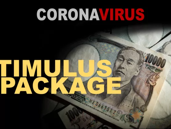
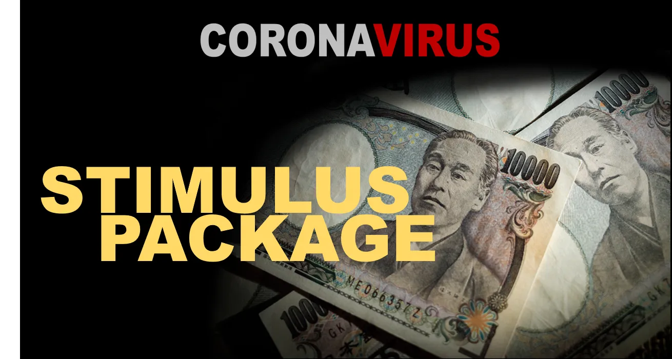
On April 16, Japan prime minister Shinzo Abe expanded the state of emergency beyond Tokyo, Osaka and five other prefectures to all 47 prefectures nationwide in an effort to curb the spread of COVID-19.As I reported two weeks ago, SEMI Japan initiated communications with all prefectural governments on April 10. Since then, the government’s concerns over the virus’s impact on the semiconductor supply chain have heightened. Prefectural Governments Plan No Restrictions on the Semiconductor Supply ChainOf the 47 prefectural governors I contacted, urging them to classify the semiconductor industry as an essential business, 40 confirmed in follow-up calls through April 20 that they have no plans to restrict operations of the semiconductor industry and supply chain companies in their jurisdictions. Those prefectures include Aichi, Akita, Aomori, Chiba, Ehime, Fukui, Fukuoka, Fukushima, Gifu, Gunma, Hiroshima, Hyogo, Ishikawa, Iwate, Kagawa, Kagoshima, Kanagawa, Kochi, Kumamoto, Kyoto, Miyagi, Miyazaki, Nagano, Nagasaki, Nara, Niigata, Oita, Okayama, Okinawa, Saga, Saitama, Shiga, Shimane, Shizuoka, Tochigi, Tokushima, Toyama, Wakayama, Yamagata and Yamanashi.However, the Aichi, Iwate, Kumamoto, Nagasaki, Oita and Saga governors cautioned they will reconsider restrictions on the semiconductor and other industries if COVID-19 transmissions worsen.The seven other prefectures including Tokyo and Osaka are not planning to respond to our request until they have COVID-19 transmission mitigation plans in place. In the meantime, SEMI Japan will continue to encourage prefectural governments to allow semiconductor supply chain companies to continue to operate unrestricted, a move consistent with current national policy for novel coronavirus disease control.Japan’s Economic Stimulus PackageOn April 6, a day before prime minister Shinzo Abe declared the emergency state for seven prefectures, he announced an unprecedented 108 trillion yen ($989 billion) stimulus package[1]. The package, equivalent to about 20% of the Japan’s economic output, dwarfs the 56 trillion yen in aid passed in the wake of the 2008 financial crisis.The first phase of the relief package seeks to halt job losses and bankruptcies, while the second will support a V-shaped economic recovery. For businesses, phase-one aid includes: Subsidies for firms that keep workers on the payroll. Large companies keeping at least half of their workers on the payroll and small and medium sized businesses that continue to pay at least two-thirds of their employees are eligible for the payouts. One-year deferment of income and regional tax payments for companies hit by the virus Property tax reductions of 50% in fiscal year 2020 for small and medium sized companies with sales that have fallen by at least 30%, and property tax exemptions for those with sales suffering contractions of at least 50%. Interest-free loans requiring no collateral for small and medium sized companies Low-interest loans available to medium sized and large companies through the Development Bank of Japan and Shoko Chukin Bank The second phase of the package, still under development, could include incentives to recharge consumer spending and tourism and subsidies for regional economies once the coronavirus has been contained.Japan COVID-19 Stimulus and Support ResourcesThe economic support measures planned by the Japan Ministry of Economy, Trade and Industry (METI) are summarized at https://www.meti.go.jp/english/covid-19/index.html#10.Prefectural and municipal stimulus and support information is summarized in Japanese at https://j-net21.smrj.go.jp/support/tsdlje00000085bc.html.SEMI Supports Members with COVID-19 ResourcesSEMI international headquarters and regional offices are here to help you, our members. For more information on our webinars, surveys, best practices and other information designed to help you meet the challenges of the pandemic, please visit the SEMI Coronavirus Updates Resources page.[1] The government increased the stimulus package to ¥117.1 trillion after a sudden policy shift to provide cash handouts of ¥100,000 for every individual in Japan. Originally, the plans were to give ¥300,000 to each household that has seen a sharp fall in income due to the virus outbreak.Jim Hamajima is president of SEMI Japan.
Read More
Japan’s Prime Minister Shinzo Abe declared a state of emergency for Tokyo, Osaka and five other prefectures[1] on April 7 in response to a startling increase of COVID-19 infections in the region’s cities in an uneasy moment for its domestic semiconductor industry. The declaration, effective through May 6, authorized the six prefectural governors to strengthen curbs on the spread of the virus and included guidance for citizens to stay home and restrictions on operations of non-essential businesses.With Japan supplying some 40 percent of the world’s chip production equipment and materials, the declaration stirred fears among semiconductor manufacturers that their uninterrupted operations – critical to sustaining the global industry – might be at risk. Japan Government Designates Semiconductor Industry as EssentialIn April 7 and 11 revisions to its Basic Policies for Novel Coronavirus Disease Control, the Japanese government allayed those concerns by designating semiconductor manufacturers essential businesses – a stark acknowledgment of the chipmakers’ vital role in combatting the novel coronavirus. The policy stated:“Among medical and manufacturing industries, we request the continuation of the following business operators in consideration of infection prevention: operators who are difficult to stop production line due to the characteristics of the equipment (such as blast furnaces and semiconductor factories); and operators who produce essentials (including important items in supply chains) for protection of the people who need medical care and support, as well as for maintenance of social infrastructure. We also request the continuation of the business operators who sustain medical care, the lives of the people, and maintenance of the national economy.”[2]SEMI Japan Reaches Out to Prefectures to Urge Essential Business Designation Equipment and materials shortages can halt production of an entire fab line and ripple through intricately connected global supply chains to stifle the production of end devices including the electronics critical to COVID-19 treatments. Electronic devices also play a central role in containing the virus’s spread by enabling artificial intelligence (AI), data analytics, digital communications, telemedicine, robotics, remote health monitoring, telecommuting, online shopping and other digital services.The essential business designation was explicit recognition that Japan’s semiconductor supply chain is integral to the global chip production ecosystem and worthy of the same protections the government has implemented for semiconductor companies. With SEMI members operating in Japan’s 47 prefectures, I sent letters to all prefectural governors three days after the second policy revision, urging them to apply the same designation, and the SEMI Japan team is following up to secure their support.SEMI Japan Encourages Government to Exempt Members from Travel Restrictions The Japan Foreign Ministry on March 31 raised to level 3 its travel advisory for 49 regions including the U.S., China, Taiwan and South Korea, encouraging Japanese citizens to avoid travel regardless of purpose to blunt the international spread of the coronavirus. SEMI Japan is working with the Semiconductor Equipment Association of Japan to urge the government to exempt semiconductor supply chain companies from the level 3 travel restrictions if they implement measures to prevent domestic infections and contagion in the visited regions. The exemptions would allow supply chain companies to install and service equipment at fabs – one key to maintaining smooth, uninterrupted operations.SEMI Supports Members with COVID-19 ResourcesSEMI international headquarters and regional offices are here to help you, our members. For more information on our webinars, surveys, best practices and other information designed to help you meet the challenges of the pandemic, please visit the SEMI Coronavirus Updates Resources page.[1] The six prefectures are Tokyo, Kanagawa, Chiba, Saitama, Osaka, Hyogo and Fukuoka.[2] Provisional translation by Ministry of Health, Labour and Welfare. Full document is available at https://www.mhlw.go.jp/content/10900000/000620733.pdf.Jim Hamajima is president of SEMI Japan.
Read More
Smart technologies have gripped the world’s imagination with their promise to revolutionize the way we live and work. With the semiconductor supply chain central to these advances, SEMI Japan in October hosted 200 members for SEMI Japan Members Day as speakers from three of the world’s top device manufacturers – Denso, Sony and Kioxia – offered their perspectives on the strides the semiconductor industry needs to make in three key areas: automotive, smart manufacturing and 3D flash memory manufacturing technology. Automotive Evolution and Electronics – DensoThe automotive industry is re-inventing itself to innovate across connectivity, autonomy, sharing and electric (CASE) and ensure safe, comfortable and environmentally friendly autonomous driving, said Nobuaki Kawahara, executive fellow and director of the Advanced Research and Innovation Center at Denso. Key focus areas of Denso in CASE innovation are Extraordinary Safety and Everyday Confidence. The company’s goal is to minimize damage to vehicles involved in collisions or one-car accidents by making it easier for drivers to detect and steer clear of objects in their path.To improve automobile safety and security, the company is developing advanced driver-assistance systems (ADAS) and autonomous driving technologies as it promotes the confluence of four areas of technology – HMI (Human Machine Interface), environmental recognition, vehicle control assistance, and information and communications. One use case Denso sees as a significant opportunity is deploying sensors such as millimeter-wave radar, cameras and LiDAR to monitor a vehicle’s surroundings, using GPS and precision mapping to pinpoint its location and determine the best route for safety and distance, and then transmitting that information to a motion-control system.Denso is also out to solve the hard challenges associated with autonomous driving in dynamic road conditions. Kawahara pointed out that road conditions vary and that rules for "driving at certain intervals in a certain lane" vary depending on the time of day. Also, on public roads in Abashiri, Hokkaido, where the company is currently conducting field tests, snowfall makes it difficult to recognize road images and gather sensor information. In Asia, it is also common for motorcycles and automobiles to speed along with very little space between them.Image Sensors to Accelerate Development of Smart Manufacturing – SonyTo fulfill the promise of smart manufacturing, the semiconductor supply chain must continue to invest in sensor and imaging technology innovation, said Shigeo Ohba, deputy senior general manager of the Imaging System Business Division at Sony Semiconductor Solutions. For its part, Sony is developing imaging sensors that help network and automate factories to achieve new production and cost efficiencies. For example, the company plans to design devices to increase equipment uptime through predictive maintenance, reduce defect rates and drive other manufacturing efficiencies. The challenge with today’s factory lines that produce a number of different devices is that they are highly complex to manage and therefore prone to human error, undercutting manufacturing efficiency. In the future, AI-powered machines will leverage data analysis to help streamline operations. Adapting an image sensor with AI to machine vision applications can simplify key processes such as measurement and inspection processes while reducing safety and security costs.Of the vast amount of information on all machines connected to the cloud, only essential details will be processed at the edge since edge data processing offers stronger security and reduces data transfer time. Ohba said image sensors will evolve based on edge AI, adding that "AI will be a paradigm shift for image sensors if it’s economically feasible."3D Flash Memory Manufacturing Technology Challenges – KioxiaIncreasing connectivity in factories for smarter, more efficient operations places huge demands on memory since networked devices typically store duplicate data, said Hideshi Miyajima, head of the Advanced Memory Development Center (AMDC) at Kioxia. To meet demand for higher networking speed and capacity, 2d NAND flash memory is moving to 3D and, in particular, three 3D techniques: multivalued memory, cell partitioning and layer stacking.To increase storage capacity, the third-generation 64-layer BiCS FLASH™ stacks layers to form nearly two trillion holes with a diameter of 100nm and a depth of 5μm on a wafer and places a uniform 2-3nm thin film on the inner wall of each 5-μm hole. For its BiCS FLASH™, Kioxia uses a dry etching technique that forms a straight, elongated through-hole and atomic layer deposition (ALD) technology, which creates a uniform laminate atomic layer on the wafer surface to grow materials uniformly and with high precision on large, complex substrates.In order to meet the cost expectations of high-volume 3D flash memory manufacturers, outlays across fabs must be reduced by better monitoring plasma control, enhancing yield through particle control, speeding film formation, and reducing gas, power and water usage, Miyajima said.SMART Transportation and SMART Manufacturing in the Spotlight at SEMICON JapanPlease join us at SEMICON Japan 2019, December 11-13 at Tokyo Big Sight, for the latest developments and trends in SMART Transportation and Smart Manufacturing. There are also a few other great reasons to attend. We look forward to seeing you in Tokyo!Jim Hamajima is president of SEMI Japan.
Read More
On July 1st, Japan’s Ministry of Economy, Trade and Industry (METI) announced updated licensing policies and procedures on the export and transfer of controlled items and their relevant technologies to the Republic of Korea (ROK). METI’s stated purpose for the actions were “in order to ensure appropriate implementation of export control.”In particular, METI will tighten controls on certain items and their relevant technologies as follows: Remove the ROK from its “white list” of trusted partners, limiting the ROK’s preferential treatment for exports Mandate individual licenses for exports of certain chemicals including fluorinated polyimide, photoresist, and hydrogen fluoride – all used in semiconductor and electronics manufacturing – and technology transferred with exports of manufacturing equipment to the ROK. Bulk licenses for the chemicals will no longer be available. METI has indicated that its actions were not intended as punitive, but rather as necessary to ensure proper management of the export control system and the effective tracking of chemicals, materials and technologies that could be used to develop weapons of mass destruction (WMDs). Nevertheless, the trade actions are cause for concern as they could have a negative impact on our members operating in Korea and Japan and the global supply chain in general.After the METI announcement, SEMI immediately consulted its International Board of Directors and assembled a global advocacy response team comprised of SEMI member companies and SEMI regional presidents in both Japan and Korea to assess risks to SEMI members operating in both regions and to the industry’s global supply chain. Additionally, SEMI conveyed its concerns to Japan and ROK trade officials, stressing that the semiconductor industry will bear the brunt of the new measures if the trade dispute escalates.SEMI president and CEO Ajit Manocha said: “We informed both governments of potential impacts of an escalation to SEMI members, their economies and the global supply chain and are encouraging them to resolve their differences. SEMI’s focus is to ensure the global microelectronics supply chain remains strong and intact.”SEMI member companies have stated that METI and the Japan government have provided assurances that trade with the ROK will not be encumbered and that semiconductor companies will see minimal impact regarding export license approvals. To this end, SEMI will continue to engage our members in Korea and Japan, monitor the dispute as it continues to unfold, and facilitate regular meetings between industry and the involved governments to ensure that industry impacts are identified and risks are mitigated. In the event the dispute escalates, SEMI is prepared to take action in accordance with its Global Trade Principles.SEMI released its Global Trade Principles last year to provide guidance to governments around the world in developing policies that benefit both regional economies and the industry. These trade principles are based on SEMI’s four trade pillars of free and fair trade, open markets, supply chain growth, and respect for IP and national security.Member companies negatively impacted by any changes in Japan’s regulatory policies or with any questions should contact their regional SEMI office or Jay Chittooran, Public Policy Manager, SEMI Global Advocacy, at [email protected] Russo is Vice President of Global Industry Advocacy at SEMI.
Read More
Wedged among four major tectonic plates, Japan is at the mercy of their abrupt herculean shifts and the earthquakes and tsunamis they can trigger. The fallout can be devastating. The magnitude 9 Great East Japan (Tohoku) temblor in 2011 and ensuing tsunami took nearly 20,000 lives, destroyed 138,000 buildings and cost $360 billion in economic damage.Factories including silicon wafer production facilities owned by Shin-Etsu Chemical and MEMC Electronic Materials – together accounting for 25 percent of the global silicon wafer production – sustained heavy damage. Operations were suspended. The Kumamoto earthquake in 2016 also caused significant damage. The economic cost: as much as $7.5 billion.With disaster risk rising on a global scale, these calamities offer valuable lessons in disaster preparedness and how companies can draw from their experiences to strengthen business continuity planning (BCP).Earthquake experiences and lessons in BCP were the focus of the recent SEMI Japan Members Day as speakers from five semiconductor device and equipment manufacturers offered their BCP strategies to about 150 SEMI members. Following are key takeaways from their presentations. Renesas: Create a robust production plant that is hard to break and easy to fixRenesas Semiconductor Manufacturing’s Naka plant took about 80 days to resume production while its ability to deliver semiconductors was delayed even longer as it recovered from damage caused by the Tohoku earthquake, said Yoshiyuki Miyamoto, Representative Director and President at Renesas. Operations at the company’s Kawajiri plant were disrupted by the Kumamoto earthquake.A key lesson from both earthquakes: The company needed to promote risk visualization from top-to-bottom in the supply chain. With the goal of making its plants easy to repair but hard to break down, Renesas implemented a risk management plan for earthquake preparedness plan to ensure stronger production line resistance and a stable supply to customers. The company ran simulations of multiple earthquake scenarios including aftershocks, enabling it to develop new BCP training and preparedness measures. Sony: Staying transparent about the disaster, sharing and interacting with related companiesYukihide Keigo, a representative from the Sony Semiconductor Manufacturing, showed footage taken the day the Kumamoto earthquake damaged a production line at its Kumamoto Technology Center. Sony is the top manufacturer of imaging sensors worldwide, and the Kumamoto plant is the backbone of that production. The magnitude of the foreshock fell within levels Sony had accounted for in its BCP at that time, and the line was expected to return to full production within a week. However, the magnitude of the earthquake that followed outstripped expectations, and the company’s BCP didn’t hold up. Three and a half months later, the plant had finally fully recovered. The protracted recovery prompted Sony to develop an earthquake preparedness plan using a model that assumed double the magnitude of expectations. For full restoration, the company identified challenges to returning to full operation at each stage of the production line. Then it went even further, developing in-house diagnostics, implementing critical path methods and strengthening earthquake resistance of equipment that manages bottlenecks for the restart of the plant. The revision of its BCP plan led to the establishment of a system to shorten the resumption of production after a major earthquake to just two months.Sony shared the contents of its BCP review with other companies to solicit help identifying any gaps and highlighted its partnership with Renesas in the Semiconductor Industry Association in Japan (JSIA), a committee of the Japan Electronics and Information Technology Industries Association (JEITA), to share materials procurement resources for the purposes of disaster preparedness and business continuity. HORIBA STEC: Steady daily practices protect hundreds of millions of yen worth of products HORIBA STEC’s Aso plant, near the epicenter of the Kumamoto earthquake, suffered heavy damage that cut off electricity and the water supply, yet production in its clean room resumed in just 10 days, said Hiroyuki Koyama, a factory manager at the plant. The plant’s quick recovery stemmed from daily preventive measures implemented before the quake such as connecting freestanding shelves for greater stability, applying thick rubber bands as rails to prevent manufactured goods from falling to the floor, and placing equipment on rolling carriages instead of fixed shelves.The practices saved the Aso plant hundreds of millions of yen in products and materials that otherwise could have been lost in the earthquake. Koyama also offered the reminder that, with regulations governing factory layout and construction differing widely depending on factors such as a building’s age, companies need to tailor their BCPs to the unique characteristics of each building. THK: The key point of dampening earthquakesTHK’s ACE Division develops earthquake dampening and vibration control devices designed to absorb the vibrational energy of an earthquake, though the devices must also be designed for precise analysis of that energy, said Hidemi Murao. Murao provided an overview of the latest technologies and products for dampening earthquake vibrations and shared test results from experimental devices.Murao described how THK’s recently introduced Linear Motion (LM) Guide, an earthquake vibration dampening technology, can significantly reduce building vibrations during a temblor. In a video Murao showed to demonstrate how the guide works, a shelf loaded with equipment rests on a platform equipped with THK’s LM Guide equipment. Simulating an earthquake, the platform shakes vigorously in every direction but the shelf remains steady as the LM Guide dampens the vibrations. The platforms can be installed on floors or underground in buildings or factories to prevent shelves from toppling. Tokyo Electron: The ideal BCP management systemOne risk associated with BCP training is that it can become overly routine, dulling the response of employees in actual disasters, said Tokyo Electron Vice President Tatsuya Aso. To help keep its workers’ skills sharp, TEL held surprise drills with employees assigned to particular BCP roles to test their ability to adapt quickly to when disaster strikes. In addition, TEL has launched surveys in more than 70 overseas locations to optimize safety in these high-hazard facilities.The SEMI Japan Members Day presentations made clear that the issue of BCP transcends boundaries between individuals, manufacturers, regions, and sectors within the global electronics supply chain. Disaster preparedness requires problem-solving across the entire supply chain, with companies sharing technical knowledge, offering mutual aid, and striving for continual improvement. Collaborative is essential. At SEMICON Japan 2019, SEMI will continue to bring companies together to address BCP initiatives and share their technical knowledge with members. Jim Hamajima is president of SEMI Japan.
Read More
Five young dancers bathed in a striking rainbow of colors with their silhouettes cast in the background dazzled SEMICON Japan 2018 attendees at the opening ceremony in mid-December. Gone were the standard opening keynotes and ribbon cutting, replaced by live performance and media art set against a dramatic black backdrop. There was no mistaking the wide-eyed looks of wonder in the audience.In its sheer vibrance, the opening ceremony thrilled with an excitement that seemed to embody the extraordinary growth expectations for the global semiconductor supply chain over the next five years, with the industry poised to double sales from $2 trillion to a staggering $4 trillion – a phenomena SEMI president and CEO Ajit Manocha has called The Rebirth of the Semiconductor Industry. Driving this unprecedented growth will be SMART applications that are transforming industries and applications worldwide, powered by artificial intelligence (AI) and Internet of Things (IoT) technologies.The dramatic scene at SEMICON Japan 2018 was staged by Rhizomatiks, a media arts company that produced the Rio Olympic Games closing ceremony and is famous for its pop music spectacles. The company’s CTO, Motoi Ishibashi, the event’s first keynote speaker, described his team’s development of drones and vehicles guided by motion and precision-control technologies. It was some of these SMART vehicles that maneuvered the opening ceremony performers from the dance company Elevenplay onstage. Only Rhizomatiks, Ishibashi said, has this capability. In its mission to enrich people’s lives through new media arts, Rhizomatiks uses the latest virtual and mixed-reality technologies to orchestrate not only dance performances but music videos, commercials, fashion shows and festivals.Toru Nishikawa, the second keynote speaker and CEO at Preferred Networks, a leading Japan-based developer of deep learning software programs, surprised the SEMICON Japan audience with his discussion of his company’s work to develop a specialized chip for deep learning processing, joining technology giants Apple, Google, Alibaba and Microsoft in chip design. As more IT and software companies develop specialized, differentiated chips, the devices are quickly becoming the heartbeat of SMART technologies. The company’s approach has taken hold. Only four years old, Preferred Networks is enjoying rapid growth by working with global powerhouses including Toyota, NTT, Panasonic, Fanuc, NVIDIA, Intel and Microsoft. Ishibashi’s and Nishikawa’s fresh visions and the media arts extravaganza reflected the success of SEMICON Japan, held again at Tokyo Big Sight: The event’s 1,881 booths – filled by 727 exhibitors from 14 regions – was the highest count in six years. With Japan home to companies that supply about 40 percent of semiconductor equipment and materials worldwide, top suppliers historically have occupied the largest spaces on the SEMICON Japan show floor.According to IDC, personal computers and smartphones, long the largest revenue sources for the semiconductor industry, will remain top revenue drivers in the coming years. But revenue from new SMART technologies for applications such as automotive and factory automation is growing, a trend expected to continue with a 2018-2022 CAGR of 9.5 percent for automotive and 5.2 percent for manufacturing, compared to 1.1 percent for PCs and 2.9 percent for smartphones.SEMICON Japan’s new SMART Applications zone highlighted these and other new market opportunities for semiconductor growth with product and technology exhibits from companies including Bosch, IBM, Microsoft, NEC, Preferred Networks, Sony, SAS, Siemens, Tesla and Toyota. But the zone wasn’t all work and no play. The ROBOT SQUARE and SPORTS x IOT robot exhibits took visitors back to their school days, with robot anime – from Astro Boy to Gundam and Evangelion – that they could ride and control! As the World Gets Smarter, So Must SEMICON and the IndustryWe all agree the world is getting smarter at a fast pace. New cars are easier to drive – some models are almost fully autonomous on highways and streets. Your SMART speaker has gone well beyond an audio playback device and is more like a home AI platform. Almost all storefronts are equipped with video cameras. Your workplace, whether an office or a factory, is driven by automation. The reliance of these environments and devices on semiconductors is driving exponential chip and changing the world. Businesses need to adapt and so do SEMICON events. We’re doing just that as SEMICON Japan 2018 demonstrated – from an opening ceremony enabled by technology innovation to new faces of the industry to the SMART Application zone. As the SEMICON Japan presidents’ reception concluded the first day of the show, a robot from the ROBOT SQUARE suddenly appeared in the reception hall in front of about 250 executives from the global industry. Everyone at the reception was impressed and stepped forward to the stage, reflecting the overall excitement about SEMICON Japan, which for many years showcased only chip manufacturing equipment and materials. This year, to keep pace with the changing world, it was much more than that.SEMICON Japan 2019 will again take place in December at Tokyo Big Sight. However, organizers of the Tokyo Olympics will be using the East Exhibit Hall usually occupied by SEMICON Japan to prepare for the games. As a result, SEMICON Japan will be held in the West and South Halls instead. Look for more changes to the event. I hope to see you next year!Jim Hamajima is president of SEMI Japan.
Read More
Artificial intelligence (AI) is on the verge of transforming entire industries as it gears up to power semiconductor industry innovation and growth, thrusting the technology to front and center at SEMICON Japan 2019, December 12-14 at the Tokyo Big Sight (Tokyo International Exhibition Center).The SMART Technology Forum at SEMICON Japan will highlight the latest AI developments and trends. Supported by U.S. Commercial Service in Japan, the forum will feature Yutaka Matsuo of the University of Tokyo. An authority on AI, Matuso will give an overview of both AI business and technology. His presentation will be followed by an AI outlook from Microsoft Japan, Amazon Web Services and DefinedCrowd.A number of Japanese startups are on leading edge of AI innovation in machine and deep learning. One is Preferred Networks Inc., a company that applies cutting-edge deep learning technology to Internet of Things (IoT) applications across transportation, manufacturing and healthcare.In his opening day keynote at SEMICON Japan, Toru Nishikawa, president and CEO of Preferred Networks, Inc., will highlight the latest developments and promise of using deep learning for industrial applications. Nishikawa will unpack how AI companies jockeying for competitive advantage will win by harnessing technologies to process massive amounts of data efficiently and quickly.Following is look at Preferred Networks, Inc. and five other Japanese startups that are driving AI innovation. Within Japan's world of AI, machine learning, and deep dearning, Preferred Networks is likely the most well-known Japanese company. The parent company, Preferred Infrastructure, was founded in March 2006 by Toru Nishikawa and Daisuke Okanohara, who focused on search engine development before turning to machine learning and establishing Preferred Networks to commercialize the technology.Preferred Networks established itself as one of the world’s top providers of machine learning technology with the development of Chainer – an open source deep learning framework that has been offered free of charge since June 2015 and was released before TensorFlow, Google’s renowned Deep Learning framework. Established in 2012, ABEJA is thought to be Japan’s first venture company to specialize in deep learning. ABEJA's core technology is its AI platform ABEJA Platform. Based on this platform, the company offers various solutions to more than 100 client companies. ABEJA also offers ABEJA Insight, a specialized package service for the retail and distribution, manufacturing, and infrastructure industries. Data analytics provider BrainPad Inc. was the first Japanese AI venture listed on the Tokyo Stock Exchange. Established in 2004, before the advent of big data, BrainPad Inc. cultivated a vision of analyzing vast amounts of data in increase the competitiveness of Japanese companies. LeapMind Inc. aims to offer deep learning technology that uses fewer computing resources and draws less power. Both are important capabilities since deep learning requires considerable computing resources to perform image and speech recognition. The company’s answer to this deep learning challenge is a small form factor FPGA with low power consumption.In April 2018, LeapMind started offering the tool DeLTA-Lite to support model construction for Deep Learning. The tool simplifies the development of deep learning design models, eliminating the need for model design, hardware, and software expertise. Hacarus Inc.’s HACARUS-X AI technology, which combines sparse modeling and machine learning technology, features low power consumption and small devices such as FPGAs. In collaboration with semiconductor trading company PALTEK, Hacarus is integrating HACARUS-X algorithms with Xilinx's FPGA Zynq UltraScale + MPSoC. Both companies area also implementing HACARUS-X algorithms in a box computer.Sparse modeling is gaining attention as a modeling method by which humans can understand the judgment process of AI by extracting features from a small amount of learning data. With expertise in life science fields such as medical and biology and image processing technology, LPixel, Inc. develops image analysis systems with original algorithms and machine learning techniques. It has developed a cloud-based AI image analysis platform and an AI medical image diagnosis support technology that streamlines the review of large amounts of research data and detects image fraud in research papers and other documents for the medical and biology fields, freeing researchers to devote more time to their core work. Yoichiro Ando is a marketing director at SEMI Japan.
Read More
On June 1st, 2018, Toshiba sold Toshiba Memory, Toshiba’s memory business, to an investment group led by Bain Capital. Toshiba Memory was then owned by a consortium of American, Japanese and Korean companies.After the long and tough negotiations, Toshiba Memory moved forward at full throttle, holding a groundbreaking ceremony for its new 3D NAND fab (100,000 WPM) in Kitakami in July and, in September, celebrating the opening of Fab 6 Phase 1 (50,000 WPM). To be sure, NAND memory is a key feature of Japan’s semiconductor industry. But the sector’s reach extends well beyond memory with its rich and versatile product portfolio nourished by active investment.Born in the early 1950s, Japan’s semiconductor industry today boasts more than 30 companies with fabs. Many feature 200mm and smaller wafer lines with legacy technologies, form factors that account for the bulk of the world’s semiconductors and are the oxygen of Japan’s chip industry. Clearly, the world is not built only with the state-of-art 7nm processed chips on the latest generation 300mm lines. Japanese chipmakers are flourishing.Automotive SemiconductorsRenesas Electronics remains a giant in microcontrollers (MCU) and system on chip (SoC) devices for automotive applications. According to IHS Markit, Renesas automotive semiconductor revenue in 2017 reached $3.6 billion while Inineon Technologies and NXP Semiconductors revenues were $3.4 billion and $3.7 billion, respectively. The three companies dominate the global automotive MCU global market. The company recently acquired Integrated Device Technology (IDT), a U.S. fabless company specializing in analog/mixed signal chips, to strengthen its automotive semiconductor portfolio. Renesas operates four volume production fabs, according to the latest World Fab Forecast from SEMI. Renesas’s microcontrollers for automotive applications (Source: Renesas Electronics) Power SemiconductorsWith power semiconductors the chips of choice for boosting the efficiency and performance of motors and batteries used in equipment, demand for the devices is rapidly growing, especially for automotive applications. Power semiconductor companies in Japan are legion and include Denso, Fuji Electric, Fujitsu Semiconductor, Hitachi, Kyocera, Mitsubishi Electric, New Japan Radio, Origin Electric, Phenitec Semiconductor, Renesas, Rohm, Sanken Electric, Sansha Electric Manufacturing, Seiko NPC, Shindengen Electric Manufacturing, Sumitomo Electric Device Innovations, Toshiba and Toyota Industries. The companies account for 26% of global power semiconductor capacity and will spend $317 million for construction and equipping in 2018.CMOS SensorsSony dominates the CMOS image sensors market with 42% share in 2016, according to Yole Développment. To meet growing demand for high-end CMOS image sensors, Sony has acquired several legacy 300mm wafer fabs and retooled them for CMOS sensor manufacturing. What’s more, Sony’s May announcement of its mid-term corporate strategy includes a 1 trillion Japanese yen investment in CMOS image sensors targeted to automotive applications by March 2021.Sony’s 7.42 effective megapixel stacked CMOS image sensor for automotive cameras (Source: Sony Corporation) MEMSMEMS is perhaps the most wide-ranging device market: Every application requires different capabilities and functions. The latest World Fab Forecast report lists 17 MEMS companies in Japan, though three makers of fast-growing RF MEMS, typically known as surface acoustic wave (SAW) or bulk acoustic wave (BAW) filters, are coming to the attention of semiconductor manufacturers. All are familiar passive electronic components suppliers – Murata Manufacturing, Taiyo Yuden and TDK – and all acquired legacy semiconductor fabs to manufacture RF MEMS.Their high-performance radio wave filters make mobile phones usable around the world. Research companies like Yole expect the introduction of 5G cellular mobile communication systems to fuel another wave of growth of the RF MEMS market. Murata Manufacturing’s SAW filters for smart phones (source Murata Manufacturing) Japanese Supply Chain Meets All Different NeedsJapan’s semiconductor supply chain provides one third of the world’s semiconductor manufacturing equipment and more than half of the industry’s materials. But Japanese suppliers also work with small and midsize makers of highly versatile chips critical to enabling the explosion of smart applications.Meet these versatile Japanese suppliers at SEMICON Japan to find solutions to your unique needs and help the world get smarter. Themed “Dreams Start Here,” SEMICON Japan 2018 reflects the promise of AI (artificial intelligence), Internet of Things (IoT) and Smart technologies. Featuring more than 750 exhibitors from around the world, the event is the gathering place to connect the people, technologies and business across the electronics manufacturing supply chain, from semiconductor manufacturing to autonomous cars, robotics and other smart applications. For more information about SEMICON Japan, visit www.semiconjapan.org.Yoichiro Ando is a marketing director at SEMI Japan.
Read More