downloadGroupGroupnoun_press release_995423_000000 copyGroupnoun_Feed_96767_000000Group 19noun_pictures_1817522_000000Member company iconResource item iconStore item iconGroup 19Group 19noun_Photo_2085192_000000 Copynoun_presentation_2096081_000000Group 19Group Copy 7noun_webinar_692730_000000Path
Skip to main content
Default Banner Image

GLOBALFOUNDRIES

Traditionally, defect classification is done manually by operators or using Automated Optical Inspection (AOI) machines, often leading to classification inconsistencies. Also, rules-based AOIs may at times be unable to fully satisfy project requirements due to the rigidity of inspection recipes. SixSense – Breaking the Status Quo with Artificial Intelligence Enter SixSense, an AI-powered defect classification software platform that has been making breakthroughs in defect detection and classification for semiconductors to make manufacturing smarter and more efficient. Founded in 2018, SixSense has already amassed a wealth of experience and chalked up a number of successes such as automating the manual image classification process, reducing manufacturing false rejects, and capturing escapees. Infineon Technologies and GlobalFoundries were amongst the early adopters of SixSense’s platform: classifAI. With Infineon, classifAI has allowed over-rejection rates to be precisely quantified. classifAI – Simple UI, Easy Usage, Powerful Models As a UI-based assistive software platform, classifAI, SixSense’s automated defect classification platform is built with the defect and yield engineer in mind. SixSense takes care of all the back-end complexities – such as coding, algorithm modelling and deployment – to enable end users to get started and use the platform with a simple GUI. The simplified end-to-end AI pipeline offered on the platform includes data labelling to make data AI-ready, model training, and model testing. Ultimately, models are deployed on the production floor for 24/7 inferencing of hundreds of millions of images every year, at scale, across processes, tools and sites. Machine learning models built by the SixSense team have seen strong results, with model accuracy of up to 98% in certain use cases. Track Record of delighting IDMs, Foundries and OSAT Customers SixSense has consistently solved visual inspection problems and enabled the success of IDMs, foundries and OSATs since its inception. The AI technology has helped a range of customers across 100mm-300mm wafer standards, both pure silicon and compound wafers, and caters to specific end-use market requirements such as RF and automotive. Partnerships between startups and established manufacturers are key to actualizing the value of AI in manufacturing. “Our collaboration with AI startup SixSense has enabled us to explore opportunities in yield gain, improving cycle time, and real-time monitoring of process shifts,” said Dato’ Tan Soo Hee, Executive Vice President, Global Backend Operations at Infineon Technologies Asia Pacific. “SixSense has been very attentive to the needs of our engineering team, addressing project requirements using a customer-first approach evident in the design of the intuitive software platform,” said Melvyn Peh, Principal Engineer, Automation-Scan-Pack, Infineon Technologies Asia Pacific. The intelligent annotation module is one of many offered by SixSense, which uses AI to train AI and accelerate the data annotation process by focusing on the semiconductor-specific requirements. Another valuable module in classifAI is advanced analytics that capture the heatmap for defect distribution on the images. Images are stacked on top of each other, with the location of defects aggregated to provide the defect heatmap. Through this, systematic failure patterns were identified that allowed defect engineers to zero in on key sources of failure and assist in root-cause analysis. Infrastructure – Scale Fast, Adapt Quickly, Accelerate Value Creation In the dynamic world of technology, machine learning and AI projects must meet changing infrastructure demands. A cloud-first approach is often favored for the plethora of benefits it offers. “We’re looking forward to a great partnership with SixSense, treading together hand in hand exploring fresh ideas and possibilities,” said Manju Jalali, Vice President of digital manufacturing at GlobalFoundries, who oversees the company-wide roll out of classifAI. For use cases where on-premise deployments are preferred, SixSense offers such options for infrastructure integration, satisfying all possible infrastructure requirements in the market. Contributing to a vibrant innovation ecosystem SixSense was mentioned by Singapore’s Deputy Prime Minister Heng Swee Keat during an event that marked Infineon’s 50th anniversary in Singapore: “I am heartened that Infineon will be investing more than $27 million over three years on an AI initiative in Singapore. Under this initiative, Infineon Singapore will be partnering academia, industry, and local startup SixSense AI to develop new AI solutions and courses.” Explosive Growth of AI in Chip Manufacturing According to a McKinsey Company report, AI contribution to semiconductor company earnings is projected to rise to between $85 billion and $95 billion per year in the coming years. SixSense has been taking great strides in creating value for their semiconductor customers. “SixSense offers tremendous value in a high-growth vertical in the semiconductor industry, marrying the latest deep learning algorithm with the compute power of the cloud,” said Rajan Rajgopal, CEO of DenseLight Semiconductor. “This leads to faster root-cause analysis that helps reduce the cost of non-conformance and improve quality.” Dominic Teo is Enterprise Business Development Representative at SixSense. He can be reached at [email protected].
Read More
Making Strides TogetherKnowledge is power – especially when it is shared. This principle formed the foundation for Micron’s Go and See virtual visit of its Singapore manufacturing plant on 26 August 2020 as 27 companies including GLOBALFOUNDRIES, ST Microelectronics, Infineon, TEL, ViTrox , IBM, HP and UTAC joined the first-of-a-kind virtual factory visit. The chip industry powerhouses gathered to see how Micron’s Lighthouse frontend wafer fabrication facility leverages Fourth Industrial Revolution technologies to drive new production and cost efficiencies.They saw clear markers of a transformed organisation and spoke with working-level staff, managers and front-line employees. Company representatives also met virtually with Micron management teams from organisations that led its digital transformation – from pilot programs to integration at scale – to realise significant financial and operational benefits. The mix of technologies they deployed to make it all happen included artificial intelligence (AI), big data analytics and the Industrial Internet-of-Things (IIoT).Micron’s Singapore-based fab facility earned Lighthouse certification earlier this year from the World Economic Forum’s Global Lighthouse Network. The Go and See tour was co-sponsored by SEMI Southeast Asia and McKinsey Company.Transformation is CrucialBy embracing Lighthouse principles, semiconductor sectors and companies can accelerate their digital transformation to boost operational and financial efficiency while helping increase productivity across the electronics supply chain. It will take time for Southeast Asia semiconductor manufacturers to transform to digital operations, though we’re seeing growing interest in Industry 4.0 practices as they begin to understand that the deployment of new technologies and applications will help them better understand real-world benefits of smart manufacturing use cases and solutions. SEMI believes shining the spotlight on companies like Micron can illuminate the way forward for other companies to help drive the industry’s digital transformation. We look forward to seeing companies build on this momentum as they start to leverage leading-edge technologies to improve efficiencies and promote sustainability.Bee Bee Ng is president of SEMI Southeast Asia.
Read More
Never before had we expected that SEMICON SEA 2020 would go virtual.The COVID-19 crisis abruptly halted our ability to hold our premier Southeast Asia electronics manufacturing exposition as we typically do – in the physical realm. The pandemic tested our adaptability, challenged our willingness to experiment and, perhaps above all, accelerated not only our own but the world’s digital transformation. We had to change our way of doing business and learn to connect virtually like we had never had before. SEMI continues to believe that virtual interaction is no replacement for face-to-face engagement. But, like the rest of the world, we fast-tracked our digital education and staged the virtual event 20 July to 21 August 2020 to gather supply chain players and help fulfill the tremendous potential of our great industry. For all the suffering the COVID-19 has caused, the pandemic has underscored an important truth – that we need innovation through collaboration now more than ever to help solve the world’s greatest problems. We thank all our event sponsors as we turned what started as a grand experiment into a successful event that drew nearly 3,000 attendees to our webinars, business matching sessions and other online offerings designed to help them uncover new business opportunities. Following are other highlights. Southeast Asia Pavilion at Virtual SEMICON West 2020 In our first collaboration with SEMICON West, our Southeast Asia Pavilion at the event welcomed virtual visitors from around the globe to help them form new connections and grow their businesses. Business Matching Sessions Technical buyers from more than 15 multinational companies along with 141 pre-qualified suppliers attended more than 50 meetings across four online business matching sessions.Technical WebinarsCompany representatives from regions including Malaysia, Singapore, Vietnam, Taiwan, the United States, the UK, Israel, China and Japan shared their expertise and industry insights at SEMICON Southeast Asia 2020 webinars. In addition, experts from leading semiconductor companies such as Micron Semiconductor Asia Operations, ViTrox Corporation Berhad and A*STAR took part in our technical exchange by sharing the latest trends in the rapidly evolving semiconductor industry. Talent Development: Inspirational University Program Talks With building the talent pipeline critical to sustaining growth of Southeast Asia semiconductor manufacturing dynamics, talent champions from Lam Research and GLOBALFOUNDRIES highlighted career opportunities and pathways for young engineers while generating recruiting leads. More than 750 students from Malaysia and Singapore engaged panelists with questions during the sessions. The SEMICON Southeast Asia team extends its tremendous thanks to sponsors and attendees for their support. As we all navigate the pandemic and hope in the near future to awaken to a brighter day, we will continue to connect virtually and, whenever possible, in person as the semiconductor industry evolves and flourishes. The SEMICON SEA 2020 team In the meantime, we will all continue to pull together to support our resilient industry as it outperforms most other manufacturing sectors. Semiconductor capital equipment shipments were up 23% globally in the second quarter of 2020 versus the same period in 2019 and semiconductor chip growth remains in positive territory. Our team has already started planning for SEMICON SEA 2021, scheduled to take place at the Setia Spice Convention Centre in Penang, 18-20 May 2021.We look forward to seeing you again soon as we continue to strengthen the microelectronics ecosystem!Bee Bee Ng is president of SEMI Southeast Asia.
Read More
Part 2 of 2Read Part 1.While companies navigate the ongoing COVID-19 crisis, corporate leaders should be evaluating a number of key business continuity issues as well as steps they can take to not only react to business disruptions but also reshape their business and recovery plans.We spoke with Dan Steele, Senior Director and the APAC Head of Environmental, Health, Safety, and Security (EHS S) at GLOBALFOUNDRIES (GF) Singapore, via teleconference for insights into the best practices he and his team have implemented from their Business Continuity Plan (BCP) to guide them through the health crisis.SEMI: How can SMEs (small and medium-sized enterprises) afford BCP, as they are often quite costly?Steele: BCP is not something you afford. Rather, it is essential to good management. Every business is about managing risks and every manager’s responsibilities include risk mitigation. Regardless of their size, companies often pay a higher price for survival in a crisis because they are ill-prepared. All companies owe it to themselves, their employees and other stakeholders to conduct ongoing business continuity planning. No one knows what or when the next crisis will be, and no plan is perfect in mitigating crisis impacts.However, it is critical to plan for potentials, institutionalize EHS and security best practices, ensure the supply chain has both redundancy and robustness, train employees to adopt additional skills, and work with customers in advance. Companies that continue to ask themselves what if are the ones that will be the best prepared. And, if BCP is done right, businesses can avoid huge losses. Dwight Eisenhower said, "Planning is everything, the plan is nothing." I think too many companies spend far too much time creating exacting plans when instead they should be planning. Since planning the survival of the company is every manager’s daily responsibility, BCP should not be purely looked upon as a cost, but also as an expected deliverable from the management team.SEMI: Companies have rolled out mandatory work-from-home (WFH) policies and it has become a new normal for many of us. What other measures can GF take should this WFH period be extended?Steele: Our work-from-home policy seems to be working quite well at this point. However, WFH will only be effective if the right tools are provided to employees – we give our employees access to our system so they can work remotely. WFH also offers opportunities to drive new and innovative ways of working, and accelerates some of our automation efforts such as Augmented Reality (AR).At the same time, mental health is just as important and we conduct weekly check-ins with employees to assess their anxiety levels by asking two basic questions: How is the team’s morale and has it impacted productivity in our operations? For us at GF, WFH is not a disintegration of the team. It is important to our operations to continue the social aspects of working as ONEGF. That means online meetings should require face-to-face interactions. It is important for people to connect. Additionally, we maintain the same quality expectations for remote work as we do when employees are on-site. If this WFH period is extended, we need supervisors and managers to reach out and ensure that we stay connected with our employees.SEMI: What BCP lessons have you learned during the outbreak and will the learnings change any of your business or operations strategies when normalcy returns?Steele: I am not sure we learned anything new about BCP. As stated, our approach to BCP is to spend less time on exact plans and more time on planning, asking ourselves what if and mentally walking our way through potential solutions. This crisis reinforces the premise that we must be prepared. We did not have a plan on our shelf for working-from-home, but we had visualized it, knew what we would have to enact and now have employees managing highly sophisticated, technical and skilled manufacturing operations from home, and some of them reside in Malaysia. BCP must be a conscientious, concerted effort even when normalcy returns – it helps us better prepare. Additionally, BCP is not the responsibility of a single person or department. Just like our daily business, BCP is an integrated effort across many functions. Good and great ideas come from anywhere in a time of crisis. Listening is extremely important.SEMI: If there is one takeaway from this unusual and uncalled experience, what will it be?Steele: What we walk away with is the fact that we are dealing with a pandemic that is highly unpredictable, and that we need all types of employees with diverse backgrounds, experiences and perspectives. This inclusion has made us successful all along, and that is what is helping us ride through this crisis today and into tomorrow. We are glad that we have a diverse and proactive BCCM team that is able to quickly adapt and respond to the many challenges of a crisis. SEMI: What advice would you offer to stay productive while WFH?Steele: We acknowledged that it is difficult for the WFH policy to be effective in the manufacturing sector. Although we do not see any productivity loss thanks to automation, we’ve seen a slowdown in our engineering activities.My advice: First stay healthy, monitor your health, and follow the government’s hygiene advice for yourself, your families and the communities you live in. If you socialized before, there is no reason to stop. Stay connected with your co-workers and team. Personally, I don’t believe WFH now means you are always on. Just as you did when working on-site, you still need your personal time. You have to strike the balance that works best for you.Dan Steele has over 25 years of experience in environmental, health, safety and security operations. He has also held other leadership roles in facilities engineering, quality, reliability and assurance, and risk management.Bee Bee Ng is president of SEMI Southeast Asia.
Read More
Part 1 of 2Read Part 2. While companies navigate the ongoing COVID-19 crisis, corporate leaders should be evaluating a number of key business continuity issues as well as steps they can take to not only react to business disruptions but also reshape their business and recovery plans.We spoke with Dan Steele, Senior Director and the APAC Head of Environmental, Health, Safety, and Security (EHS S) at GLOBALFOUNDRIES (GF) Singapore, via teleconference for insights into the best practices he and his team have implemented from their Business Continuity Plan (BCP) to guide them through the health crisis.SEMI: How did GLOBALFOUNDRIES Singapore first respond when the country reported its first COVID-19 case?Steele: Since the early days of our company, we have had a Business Continuity / Crisis Management (BCCM) team in place that is responsible for business continuity planning for the site. At the beginning of this journey with the coronavirus, we believed in two truths: maintaining the safety and well-being of our employees and consistently communicating precautionary measures the company has taken to protect them and our business. These actions are critical to keeping our employees safe, while keeping the anxiety level low. By informing and updating employees in a timely manner, we ensure that they are well-educated about the crisis as it unfolds and the foreseeable circumstances that could be ahead of us. Once the world was well into the coronavirus outbreak, our CEO declared in a message to all employees that “we entered this pandemic crisis together, and we will exit it together.”We have also established links to pertinent government websites and made them conveniently available to ensure employees have access to the latest available information for their personal lives.SEMI: What actions has GF Singapore taken in response to the crisis so far?Steele: On January 29, our BCCM team activated the first line of defense by initiating temperature checks at all building entrances for every individual including employees, contractors, visitors, and customers who come into our facilities. We asked each to declare their state of health and travel history and issued a temperature card to every employee and resident contractor. They are all required to record their temperature twice daily – once before coming to work and again at midday – and they present the temperature log to security upon their arrival.The following week, our teams split into an A/B work arrangement to ensure continuity of our operations. We proactively pared down our teams to the staff essential for our on-site operations, while enabling the rest to work from home. We also advised our most vulnerable employees with impaired immune systems or who are pregnant to work from home. Concurrently, we moved all meetings of 10 or more people to virtual communications and only allowed meetings with fewer than 10 to be held in rooms with participants sitting at least one meter apart. We informed our customers of our efforts and moved all planned on-site visits to online visits.In line with Singapore’s efforts to curb the spread of COVID-19 within the community, GF restricted site access of people who had recently traveled to countries with sustained community transmission and regularly updated the restriction list. To conduct contact tracing, we created our two degrees of separation list that we used to track employees with families and close associates who were linked to a COVID-19 case. Employees provided the information voluntarily. On our campus, we enforced strict safe distancing measures by limiting access to meeting rooms, marking off-limits tables and removing chairs in the cafeteria, limiting the number of elevator riders to no more than four, and placing boxes or other spacing indicators at smoking zones, bus stops and temperature-taking lines. We also initiated a daily log of employees taking the company buses tagged to the bus number, time, and employee identification numbers in anticipation of the need for contact tracing.Most recently, when the Singapore-Malaysia border closed, we activated the next phase of our BCP that was already in place – housing over 450 Malaysian employees in Singapore hotels.Throughout this crisis, we continuously monitor and evaluate possible impacts to our supply chain to ensure the continuity of our business. This is a standard element of our ongoing business continuity management system.Most importantly, we frequently communicate with our employees and tell them everything the company is doing and why we are doing it. We encouraged employees to monitor their health, stay home if they are unwell, and seek immediate medical treatment if necessary at one of our panel clinics or other medical facilities.SEMI: What are your top concerns amidst this health crisis?Steele: At GF, we are managing through the crisis with an unwavering focus on two guiding principles: the safety and well-being of our worldwide team, their families and communities; and delivering on our commitments to our clients. As the world’s leading specialty foundry, GF has a unique role in the global supply chain. Our semiconductor technology is vital to a range of industries including health care, communications, infrastructure and security. With these priorities in mind, the company undertook unprecedented steps and has adapted to the crisis by dynamically adjusting its protocols, health and safety measures, and business processes to protect its teams while maintaining manufacturing excellence.We are committed to safeguarding the well-being of our employees while supporting and sustaining our on-site operations and protecting customers’ products. A major concern is the impact on our employees. We understand that COVID-19 can be infectious even if an individual is asymptomatic – we are always concerned that temperature screening alone is not sufficient. This is the reason that from day one we have encouraged our employees to monitor their health, follow all government advice for proper hygiene and seek medical attention if unwell as early as possible, and not come to work.Dan Steele has over 25 years of experience in environmental, health and safety, and security operations. He has also held other leadership roles in facilities engineering, quality, reliability and assurance, and risk management.Bee Bee Ng is president of SEMI Southeast Asia.
Read More
Imagine a world where there are chips in about everything we touch on a daily basis. It is not hard to do with semiconductors already at the core of many leading-edge electronic devices. These sophisticated chips are hidden from sight, but their functions are vitally significant to our daily lives.Manufactured in multibillion-dollar facilities, the production process of chips is one of the riskiest, costliest, and most technically complex feats in business. Consider the difficulties of managing contaminants during device manufacturing: A single speck of dust on a lens could cause the entire output of the plant to be scrapped.For years, these exotic fabrication facilities, called fabs, have been packing more efficiency into ever smaller chips. As new technologies continue to emerge, chip manufacturers face constant pressure to continually refine and improve their operations to meet the challenge of rising device performance and yield goals. Fab managers must optimize tool performance, improve fabrication techniques, safely handle toxic materials and design better integration flows. Layer on top of those requirements customer demand for greater innovation and quality of service, it can be difficult for manufacturers to handle everything on their own while consistently meeting necessary requirements.Align for CollaborationWith the help of the Fab Owners Alliance (FOA), a SEMI technology community, manufacturers and their suppliers don’t have to travel this road alone. Membership in this international group allows semiconductor and MEMS fab managers and industry suppliers to come together to solve common non-competitive manufacturing issues and improve business results.Founded in 2004, the group consists of 25+ device manufacturers (DMs) with over 120 semiconductor manufacturing facilities and 60+ solution providers (SPs) who supply equipment and services. Through quarterly meetings, study teams, benchmarking surveys, case studies and online forums, FOA successfully provides a collaborative, non-competitive platform to the fab management and operations community. FOA members enjoying an engaging discussion and networking event during the recent Q1 2019 Collaborative Forum at the Double Tree Resort in Scottsdale, Arizona One of the most popular FOA platforms is the annual Collaborative Forum early in the year. The goal is to bring together DMs and SPs from around the world for an open dialogue under one roof. For two days, they share success stories and discuss issues facing their fabs and the industry in general and develop collective strategies to address them.The success stories are particularly engaging as they accentuate the value and benefits of FOA membership. Presented as case studies, these stories outline how the DMs and SPs work together to improve fab efficiency and increase yields. Often, the ideas for the case studies are conceived during networking events, fab tours and programs organized by the FOA.The case studies shared at the 2019 Collaborative Forum, held at the Double Tree Resort in Scottsdale, Arizona, February 13-14, 2019, illustrate the power of collaboration within the FOA. Following are a few examples.Scheduling System Implementation Broadcom was facing a steep ramp when it decided to engage with FPS, an INFICON product line. In addition, the manual decision making, and limited real-time visibility of factory data was negatively impacting their production in its 150mm and 200mm environment. By deploying an integrated Smart Manufacturing software solution and its digital twin, FPS was able to retrofit Broadcom’s manual factory with automated decision-making capabilities.This solution offered many benefits. Constraint tool utilization increased by more than 15 percent. The automated WIP management system also eliminated many manual wafer handling issues such as lost lots, WIP storage constraints, building transfers, and time spent looking for lots. Pushing Tool Performance BoundariesAs tools in the 200mm space are hard to find, GLOBALFOUNDRIES is always looking to squeeze every wafer out of its existing resources. To drive continuous improvement and increase equipment throughput, GLOBALFOUNDRIES leveraged MAX’s knowledge with Machine Rate Models. Together, they were able to employ a modelling technique that helped them model key toolsets and develop actions to increase intrinsic machine rate performance.Based on this knowledge, 10 capacity constraints were selected, and speed models were developed for all of them. This win-win collaboration allowed GLOBALFOUNDRIES to find some real opportunities that translated into CAPEX and cost savings. On average, the companies identified a 12 percent potential improvement opportunity per toolset and created engineering task force teams to prioritize and drive the improvements.Simplifying the Chamber Matching Process Using Trace AnalyticsThe collaboration between NXP and BISTel resulted from a shared vision of achieving Smart Manufacturing using analytic solutions enabled by artificial intelligence and other advanced technologies. Chamber matching is critical in identifying process variation to ensure manufacturing quality. Traditional tools like Fault Detection Classification (FDC) often do not provide clear enough insights to pinpoint the issues and require extensive time to collect data from each chamber.Through several use cases, NXP and BISTel successfully illustrated the effectiveness of using a trace analytic solution to quickly and accurately quantify and monitor chamber-to-chamber mismatches as well as changes within a chamber over time. The full trace analyses of all parameters allowed NXP to generate better FDC models to more quickly detect similar issues in the future. In addition, NXP was able to identify the cause of a parametric shift by comparing performance of the same chamber between two different time periods. All in all, the trace analytics solution brought together and analyzed the process data efficiently, thereby reducing analysis time from days to minutes.Eagleview Inspection of SiC and Transparent Wafers X-FAB challenged Microtronic to develop a new capability for its high-throughput recipe-less macro defect inspection systems. Microtronic’s EagleView machine vision macro defect inspection system is well known for its versatility in the semiconductor industry due to its wide deployment as well as its recognition as winner of the 2017 Best of West Award at SEMICON West. But X-FAB’s requirements to inspect and image transparent wafer substrates were novel. After working closely to understand X-FAB’s needs, Microtronic made extensive hardware and software enhancements to enable high-throughput macro inspection of Silicon Carbide (SiC) and other transparent wafer substrates.Get InvolvedThe FOA meetings are held at device manufacturing sites twice a year. The next meeting will be graciously hosted by MACOM in Lowell, Massachusetts, May 22-23, 2019. The DMs and SPs will meet again at SEMICON West at the Moscone Center in San Francisco on July 11, 2019.To attend these meeting and be part of this high-impact group, please email us at [email protected]. For more information about FOA, please visit our website.Nishita Rao is a marketing manager at SEMI.
Read More
Christian G. Dieseldorff, Industry Research Statistics Group, SEMI (June 12, 2018)The semiconductor industry is nearing a third consecutive year of record equipment spending with projected growth of 14 percent (YOY) in 2018 and 9 percent in 2019, a mark that would extend the streak to a historic fourth consecutive growth year, according to the latest update of the World Fab Forecast report published by SEMI. The industry last saw four consecutive years of equipment spending growth in the mid 1990s.Korea and China are leading the growth, with Samsung dominating global spending and ascendant China on a fast, steep rise, surging ahead of all other markets. See figure 1.Figure 1: equipment spending by region (includes new and refurbished)Samsung is expected to reduce equipment investments in 2018. Despite the ebb, the company still accounts for a dominant 70 percent of all investment in Korea. At the same time, SK Hynix is increasing its equipment spending in Korea.China’s equipment spending is forecast to jump a whopping 65 percent in 2018 and 57 percent in 2019. Notably, 58 percent of investments in China in 2018 and 56 percent in 2019 stem from companies with headquarters in other regions such as Intel, SK Hynix, TSMC, Samsung, and GLOBALFOUNDRIES. Domestic, Chinese-owned companies – backed by large government initiatives – are building an impressive number of new fabs that will start equipping in 2018. The companies will double their equipment investments in 2018 and again in 2019.Meanwhile, other regions are also ramping up investments. Japan is beefing up equipment spending by 60 percent in 2018, with the largest increases by Toshiba, Sony, Renesas and Micron.The Europe and Mideastern region will boost investments by 12 percent in 2018, with Intel, GLOBALFOUNDRIES, Infineon and ST Microelectronics as the largest contributors. Southeast Asia will increase investments by more than 30 percent in 2018, although total spending is proportionately smaller than in other regions owing to its size. The main contributors are Micron, Infineon and GLOBALFOUNDRIES, though companies including OSRAM and ams are also increasing investments.The SEMI World Fab Forecast, which also includes information on other companies, covers data and predictions through the end of 2019, including milestones, detailed investments by quarter, product types, technology nodes and capacities down to fab and project level.Learn more about the SEMI fab databases at:www.semi.org/en/MarketInfo/FabDatabase and www.youtube.com/user/SEMImktstats.
Read More
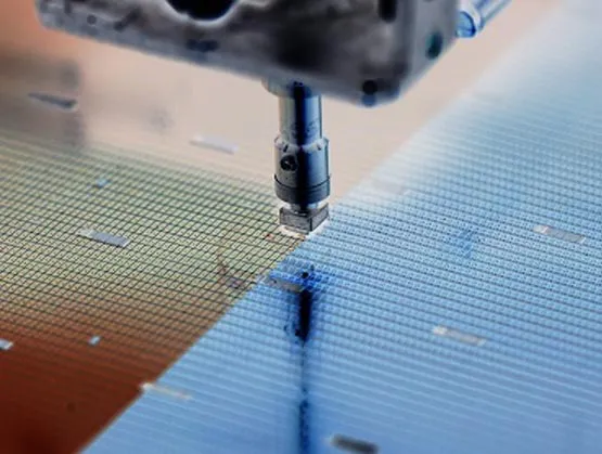
This year’s Advanced Lithography TechXPOT at SEMICON West will explore the progress on extreme ultra-violet lithography (EUVL) and its economic viability for high-volume manufacturing (HVM), as well as other lithography solutions that can address the march to 5nm and onward to 3nm. Several session speakers offered their insights into the readiness of EUVL for 5nm and how other lithography solutions will enable 3nm. See the full list of speakers and program agenda at http://www.semiconwest.org/programs-catalog/lithography-5nm-and-below.Diverging viewpoints on EUVL readiness for 5nmMike Lercel, Director of Strategic Marketing at ASMLASML expects its first customer to start volume manufacturing with EUV at the 7nm logic node and the mid-10nm DRAM node in the 2018/2019 timeframe. “EUV will replace the most difficult layers that require multiple patterning, and many layers will continue to be allocated to immersion tools for the foreseeable future,” said Lercel. “For the 5nm logic node, more layers are expected to migrate to EUV.”Three ASML customers have early-access versions of the next-generation TWINSCAN NXT:2000i for the development of advanced logic and DRAM nodes. “This system delivers 2.0nm cross-matched on-product overlay, achieved through several hardware advancements,” noted Lercel. “It is also significant because this mix-and-match use with EUV features a significantly different hardware platform.” TWINSCAN NXT:2000i features a new alignment sensor and improved wafer table flatness, endurance, and clamping mechanism to enhance matching to EUV.ASML has achieved good industrialization progress of its pellicle, with tests confirming that pellicles can withstand 245W source power and an offline power lifetime test indicating 400W capability. Compared to the 7nm logic node, the requirements for EUV masks will become tighter at 5nm, but Lercel noted that ASML sees good progress with the industry infrastructure to support 5nm in areas such as reducing mask blank defects. “We will continue to improve pellicle transmission for enhanced throughput, but there are no fundamental changes in pellicle requirements for 5-3nm logic nodes. We see no infrastructure showstoppers for the introduction of EUVL at the 5nm node.”Stephen Renwick, Director of Imaging Physics at Nikon Research Corporation of AmericaRenwick said that the 7nm logic node is expected to be fabbed mostly using 193i lithography. “EUV will struggle to be ready for 5nm, limited by yield issues caused by stochastic effects in the resist,” said Renwick. “Ready or not, though, it will be used.” Renwick suggests that introducing multiple-patterning with EUV may be needed but would increase costs. “193i lithography will continue to be used with quadruple-patterning and in combination with other techniques – there is no single solution.”Figure 1. Normalized cost/layer vs. lithography method. SOURCE: Nikon Research Corporation of America When choosing between immersion lithography and EUV for different customer segments at 5nm, Renwick noted that the cost depends on the layer. “Some time ago, we calculated that the costs of either 193i triple-patterning or 193i SADP with two cuts were roughly equal to single-patterning with EUV,” explained Renwick (Figure 1). “That agreed with chipmakers' public estimates and meant that the choice of lithography method depended more on the performance tradeoffs involved, such as 193i's better line-edge roughness. At the 5nm node, we are probably faced with quad-patterning from 193i, double-patterning from existing EUV tools, or single-patterning from as-yet undelivered high-numerical aperture (NA) EUV tools.” Renwick believes that the competition between low-NA EUV double-patterning and 193i quad-patterning will be similar to the current situation (i.e., comparison of 193i triple-patterning or 193i SADP with two cuts vs. single-patterning with EUV), but for high-NA EUV tools he believes it's too early to say.Other challenges Renwick sees on the horizon for EUVL at 5nm are stochastic effects in EUV resists. “They cause yield problems on contact arrays and unacceptable line-edge roughness on line/space patterns,” said Renwick. “It's unlikely that these effects will go away without increasing the litho dose, which will further challenge throughput performance.” He also questions whether EUV pellicles, though under development, will be “ready for prime time.”Harry Levinson, Sr. Director of Strategic Lithography Technology and Sr. Fellow at GLOBALFOUNDRIESLevinson said additional fundamental engineering work is needed to ready EUV lithography for 5nm. “Among the top problems are stochastics-induced resist defects, which increase significantly as dimensions shrink below those for 7nm,” explained Levinson (Figure 2). “Higher exposure doses will be required to address these issues related to stochastics at 5nm, which will require higher source output” (than 7nm).Levinson said there will be greater motivation to use EUVL at the 5nm node vs. at 7nm to offset the large number of exposures associated with 193nm immersion multiple-patterning solutions. “The primary application of EUV lithography at 7nm will be for contact, via and cut layers,” Levinson noted. “It will be important to enable EUVL for metal masks at the 5nm node, which increases the need for an ample supply of very low defect EUV mask blanks.” Levinson added that the 7nm node is already stressing defect inspection capabilities, and no actinic defect inspection system is yet available for patterned masks. “This situation becomes more problematic with widespread application of EUVL to metal layers.” Mask development for 5nmChristopher C. Progler, CTO Strategic Planning at PhotronicsProgler said that the basic infrastructure for delivering EUV masks is available, especially for dark field layers and near in nodes. “The interconnected or more open frame patterns will need refinements to the processes and two to three nodes out will need certain new infrastructure,” said Progler. Overall, the main challenges for initial insertion are about creating a cost-effective and rapid-turn EUV mask process, he said. “The industry can certainly deliver EUV masks in some form. It is more a question of doing it efficiently and productively to match the stated value proposition of EUV over other lithographic methods. We don’t want a pick two of ‘cost, cycle time, capability’ sort of mask solution.” More specifically, Progler explained that after the initial EUV mask development for 5nm focused on contacts and block layers, the major push for N5 switched to delivering single-exposure EUV metal patterning as early as possible. “This has opened some new challenges for masks given the resolution, critical pattern density and tight pitch defect requirements of the re-aggregated single-layer metal mask designs,” said Progler. “For example, on the resolution side, we are accelerating the insertion of higher dose photoresists and also driving patterning module improvements in CD control, mask LER and sidewall angle.” Progler added that at N5, the mask 3D structure itself – including the sidewall – will have a greater impact on lithography because it is tied to stochastic error rates on the wafer.“Reliable, wide-area metrology for some of these 2D and 3D mask parameters is currently hard to come by. We may see an evolution of the blank structure at some point in N5, including hard mask options for pattern stability and expect earlier insertion of EUV mask process correction with model-based hot spot detection and rule checking as well. We also hope mask-scanner dedication is not needed, but there are some indications process sensitivity may push us earlier in this direction.” He added that to reduce metal layer defects, more attention needs to be devoted to advanced repair and model-based validation. “We are, unfortunately, still in a situation of blurry vision and high native defect counts alongside possible in situ contamination during mask changes.” Figure 2. Resist stochastics-induced defects. Graph courtesy of Peter DeBisschop, imec; SOURCE: GLOBALFOUNDRIES Progler pointed out that, with the advent at 5nm, metal masks will require some level of actinic blank inspection for yield, increasing the cost of an already expensive mask technology. “So, unless we want to contend with double and triple photomasks’ starts to deliver a single metal layer, it will be very important to tighten the multi-sensor inspection, defect abatement, and repair loops,” said Progler. He does see some clouds forming around high-volume manufacturing pellicles for metal layers. “This remains an open question, mainly for thermal and materials reasons, not to mention cost and cycle time,” Progler said. “We may be pessimistic, but we do not see an HVM pellicle solution converging in the required timeframe, which means leaning even more on a wafer-level inspection in the validation loop.” He believes that streamlining validation will be a differentiator. “I can imagine one losing most of the EUV cycle time benefits by endlessly circling masks around if this is not done well.” How does the industry get to 3nm? ASML plans to ship its first high-NA EUV prototope/pilot systems between 2020 and 2023 to support 3-2nm process development. “System designs are now being finalized and the platform is starting to come to life,” said Lercel. ASML supplier ZEISS is building a high-NA cleanroom for optics production. ASML believes that EUV, high-NA and DUV systems will be used together at the most advanced nodes and is designing to account for this mixed environment. “As chipmakers drive toward smaller geometries in the most advanced nodes like 3nm, they face unprecedented challenges in devices and materials. This will make the process control requirements even more challenging.” ASML is tackling these challenges with its YieldStar metrology platform, e-beam metrology (HMI) and computational lithography solutions that are designed to expand the process window, enhance process control, and improve patterning defect detection. “This ‘Holistic Lithography’ approach will become increasingly important to ensure throughput and yield at the most advanced nodes.”Levinson said that the issues he projects for 5nm will need to be addressed further at 3nm. “The challenges associated with resists at 3nm dimensions are such that it isn’t clear that chemically amplified resists will be capable of meeting requirements,” said Levinson. “If true, we would be seeing the most significant change in resist platforms in a quarter of a century. Potentially cost-reducing technologies such as directed self-assembly (DSA) are always welcome, but EUVL will be the lithographic workhorse through the 3nm node, and likely beyond.”At 3nm, mask makers will confront the realities of higher EUV NA tools. “We will need to implement thinner mask absorbers, new films, and perhaps hard masks,” Progler said. “This puts us in a new materials regime for masks, and history has shown us the mask industry takes a long time to refine processes and tools for new mask materials.” He explained that the small scale of the mask ecosystem and the small number of large suppliers available to address the challenges accounts for this lengthy time frame. Still, looking ahead, Progler noted that Photronics has already done a few studies on the impact of proposed half-field, high NA anamorphic optics on masks. "We uncovered some challenges that need to be addressed, particularly at boundaries and within the overall mask flow,” said Progler. As mask resolution continues to scale down, the industry will need fundamentally higher resolution mask making and inspection processes, requiring next-generation multi-beam mask writing and electron beam inspection, he explained.At 3nm and below, Progler noted that the metrology needs for masks, while not as severe as that for wafers at these nodes, will test the mask equipment infrastructure in ways that could challenge the relatively small mask industry. “Of course, EUV multi-patterning comes into play as well, and with that, the SRAF sizes will drop below 20nm, requiring an asymmetric compensation over a much wider influence area than the OPC people are used to considering.” With EUV multi-patterning, Progler explained that it will be increasingly important to match or pair EUV masks and to consider how 3D effects and stochastics will drive new technology to enable new requirements for high-speed metrology and simulation components. “All the justifiable hand-wringing over EPE with ArF multi-patterning today gets introduced to the EUV scene when masks are ganged together to make a single device layer,” said Progler.Debra Vogler, SEMI
Read More