downloadGroupGroupnoun_press release_995423_000000 copyGroupnoun_Feed_96767_000000Group 19noun_pictures_1817522_000000Member company iconResource item iconStore item iconGroup 19Group 19noun_Photo_2085192_000000 Copynoun_presentation_2096081_000000Group 19Group Copy 7noun_webinar_692730_000000Path
Skip to main content
Default Banner Image

SEMI News

With chipmakers looking toward 5nm manufacturing, it’s clear that traditional scaling is not dead but continuing in combination with other technologies. The industry sees scaling enabled by 3D architectures such as die stacking and the stacking of very small geometry wafers. Interconnect scaling also comes into play. This year’s Scaling Technologies TechXPOT at SEMICON West (Scaling Every Which Way! – Thursday, July 12, 2:00PM-4:00PM) will provide an update on the evolution of scaling and describe how the various players (foundry, IDM, fabless, and application developers) are jockeying for innovation leadership. As a prelude to the event, SEMI asked speakers to provide insights on important scaling trends. For a full list of speakers and program agenda, visit http://www.semiconwest.org/programs-catalog/scaling-every-which-way.Challenges for gate-all-around (GAA) and FinFET devicesDiederik Verkest, imec Distinguished Member of Technical Staff, Semiconductor Technology and Systems“During the processing of GAA devices, there are ‘non-line-of-sight’ hidden features that are difficult to control and characterize and may also lead to new defect mechanisms that would impact yield, and possibly product reliability.”Common performance boosters for gate-all-around (GAA) FETs and FinFETs include lower access resistance, lower parasitic capacitance, and stress. “However, one specific performance booster that only applies to GAA is the reduction of the spacing between the vertical wires or sheets,” says Diederik Verkest, imec distinguished member of technical staff, Semiconductor Technology and Systems. “This reduces parasitic capacitance without affecting drive current and hence benefits both performance and power.” He further notes that imec demonstrated the first stacked gate-all-around (GAA) devices in scaled nodes. “In fact, we are the only ones that published working circuits – ring oscillators in a scaled node using industry-standard processes – in our case replacement metal gate (RMG), and embedded in situ doped source/drain (S/D) epitaxy.”“There are two elements of the stacked GAA architecture that need to be addressed,” says Verkest. “The first is that this architecture uses epitaxially-grown layers of Si and SiGe to define the device channel. The use of grown materials for the channel and the lattice mismatch between the two materials represent a departure from the traditional fabrication of CMOS devices, so the industry needs to develop and gain confidence in novel metrology that allows for good control of the layers and also proves their low defectivity.” The second aspect is the three-dimensional nature of the GAA devices. “During the processing of these devices, we have ‘non-line-of-sight’ hidden features that are difficult to control and characterize and may also lead to new defect mechanisms that would impact yield, and possibly product reliability.”Huiming Bu, Director, Advanced Logic/Memory Research - Integration and Device, IBM Research, Semiconductor Group"A new device architecture beyond FinFET is required to provide a full technology node scaling benefit (i.e., density, power and performance) at 5nm and 3nm.”Huiming Bu, director, Advanced Logic/Memory Research - Integration and Device, IBM Research, Semiconductor Group, says that naming of technology nodes has been used extensively for marketing strategies in “foundry land,” but the designations have lost much of their meaning as technology scaling differentiators. “That said, when it comes to technology innovation and value proposition, IBM, in conjunction with Samsung and GLOBALFOUNDRIES, has developed the GAA NanoSheet transistor for 5nm to provide a full technology node scaling benefit in density, power and performance,” says Bu (Figure 1). The key parameters for intrinsic device optimization when scaling to the 3nm node, explains Bu, are the NanoSheet width for better electrostatic characteristics, and the number of sheets for increased current density. Also necessary are strain engineering for carrier transport enhancement, and interconnect innovations for parasitic RC reduction. “Beyond that, the industry needs to look into something different, something more disruptive.”Figure 1. TEM cross section of stacked NanoSheet transistors. SOURCE: IBM Research Materials challengesMaterials challenges are also a concern as the industry moves to 5nm and below. “We see increasing complexity in the material systems that are being used,” explains Verkest. One example he cites in scaled FinFET or GAA technologies is the use of two to three layers of different materials – typically metals such as TiN – to which small amounts of other elements are added to set device characteristics such as the threshold voltage. “At the same time, the requirements for the thickness of these materials, driven by gate dimensions for example, or the distance between the wires, are increasingly challenging.” Other examples of materials challenges are the use of two to three different types of insulators in the middle-of-the-line, each with different etch contrasts. “We use novel materials such as carbon containing oxides or oxynitrides that have lower dielectric constants in order to boost the performance of circuits,” he says, noting that the materials list “is quite long.”Several critical dimensions in transistors at advanced technology nodes have already reached a few monolayers of atoms, fueling expectations for innovation at the material level for transistor scaling, Bu notes. “The other argument is that there is a growing gap between computing demand and the slowdown of technology advancement driven by conventional scaling,” says Bu. One trend that addresses this gap is integrating more computing functions that make the technology solution more modular, which naturally leads to the incorporation of more materials for more applications. Bu cautions, however, that introducing new materials in semiconductor technology has never been easy. “It takes many years of R D to reach this implementation point, if it ever happens. So, do we need new materials when the industry moves to 5nm and 3nm? Yes, though I expect new material implementation to be a lot faster in interconnect and packaging at these nodes rather than intrinsic to the transistor.” Challenges in developing atomic-level processesThere will be challenges in developing atomic-level processes used in scaling, such as atomic layer depositions (ALD) and atomic layer etches, notes Verkest. “These classes of processes are both required to handle the scaled dimensions at the 5nm and 3nm nodes, and also the 3D nature of the scaled technologies – and here we are talking about logic and memories,” Verkest says. “With respect to depositions, we would need to develop thermal ALD processes (not plasma-based) that enable accurate and conformal depositions in non-line-of-sight structures.” Adhesion and wetting, smoothness, and throughput would also need to be addressed. “Longer term, these processes need to facilitate selectivity and self-alignment to address gap-fill challenges in highly scaled structures,” he says. Other concerns he notes with respect to atomic layer etches are selectivity to various materials, and fidelity requirements that increase the requirements for metrology accuracy. “Throughput is also a concern.”Bu believes that a new device architecture beyond FinFET is required to provide a full technology node scaling benefit (i.e., density, power and performance) at 5nm and 3nm. “Beyond 3nm, we may need to continue the transistor scaling in the vertical direction and start to stack them together,” Bu says. He also cites the need for parasitic R/C reduction in the interconnect to take advantage of the intrinsic transistor benefit at the circuit and chip levels. “We see a lot of opportunity in atomic-level processes, especially in atomic layer etch and selective material deposition, to address these challenges in the transistor and the interconnect.” Debra Vogler, SEMI
Read More
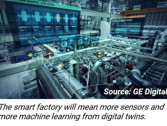
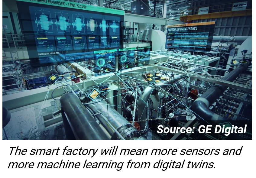
The fast-maturing hardware and software that are enabling practical applications of equipment intelligence and machine learning mean disruptive change for microelectronics manufacturing. But first comes the basic work of building the basic infrastructure, figuring out IP separation, and learning to solve physical problems in the digital world. Just how much can the semiconductor industry leverage industrial IoT practices from other industries? Common wisdom may be that industrial software solutions aren’t well suited to the IC sector’s complex needs. But GE Digital enterprise account executive Luke Smaul, currently working with Intel, argues that semiconductor fabs and toolmakers are dealing with similar issues as GE did when it first started working with Delta Airlines to monitor the GE engines on Delta planes. Smaul will speak at SEMICON West about GE’s work with Intel over the past few years and, in particular, how its solution for cloud security and IP separation can work for ICs. “GE learned to provide IP security and separation in the aviation space with its suppliers, which moved us all up the value chain, providing a big engine for growth,” says Smaul, who started his career as an IC engineer. “GE Aviation saw a 25 percent increase in issue detection rates by leveraging the same common platform. We’ve shown that we can protect Intel intellectual property in its own cloud space and control who can access what.” A toolmaker can access only particular fab data as needed for analysis, and then can reveal only the output from the analysis and a subset of supporting data. “IP separation has to happen, and it will unlock huge added value,” Smaul says. GE’s Predix solution aims to supply an easy-to-use, plug-and-play system for analytics to enable a yield engineer without a deep data background to select a supported sensor, a gateway to connect automatically to the cloud, and an analytics application to test a hypothesis of how the collected data relates to yield. “This empowers the yield engineer to use and unlock information for a quick improvement, even for simple things such as looking at the impact of degradation of fan performance over time on yield,” says Smaul. “Though the scope may be small, the impact on yield in aggregate, and when scaled, is large.” “There needs to be much more collaboration across the industry to make this work, and to share best practices,” says Smaul. “Just as GE moved from selling gas turbines to selling power-as-a-service, vendors of other big, expensive assets like IC equipment will likely change their business model from selling tools towards selling yield-as-a-service. This will simplify life for the fab while bringing the toolmaker more opportunity to sell improved capabilities on existing tools.” More human intelligence makes AI smarter Applying AI neural network approaches such as deep learning to predict outcomes from digital models is enabling disruptive advances in speech and image recognition, but applying it to complex IC manufacturing problems such as predictive maintenance has been a challenge. These neural networks require massive amounts of data to train, and the IC sector doesn’t really have big data, just a lot of little data clusters due to the dynamics and context richness of processes. This data is difficult to combine for analysis. In addition, the neural network provides only an answer but can’t explain why, notes Michael Armacost, managing director of advanced service engineering at Applied Materials. “We’ve learned that it works better if we do not ignore what we know already, but rather incorporate expert knowledge in a structured way to help us focus on the key features and the key data,” says Armacost, who will also speak in the program. This includes choosing the most important steps to include in the model, identifying the limited data to collect and how to filter the data for outliers, and then selecting the final parameters and features, adjusting the limits, and making adjustments as results drift change over time. The less data needed, the better for the complicated issue of IP protection as well. The big gains from these new analysis approaches will likely require data from more than one company and supporting security for remote connectivity. “Some end users are attempting to do the AI all themselves, but in the long term there will need to be collaboration across companies,” says James Moyne, University of Michigan professor and consultant to Applied Materials, another speaker. Collaboration will need to balance the value of the solution against the risk of compromising IP. “The low-hanging fruit are applications such as predictive maintenance in areas that do not involve high-priority IP. Another approach will be to limit the amount of shared data needed – to first build the model on a wide range of data, but then to use only a very small amount of data to operate the models.” Ready-made models could speed the process Coventor’s semiconductor process models are finding initial applications in R D whereby companies use the simulation to understand the effect of process variation on their complex designs. Instead of running dozens of actual wafers to optimize semiconductor processes, users can instead quickly simulate the results of complex process interactions on their design. Going forward, the process models could find a wide range of applications, from accelerating stabilization of new processes in the fab to enabling real-time co-optimized control across previously independent unit steps to improve wafer uniformity. “This improved uniformity across wafers and equipment could potentially reduce the need for costly physical silicon validation,” suggests Joseph Ervin, Coventor director, semiconductor process and integration, another SEMICON speaker. “Making use of in-situ metrology for real-time control also demands a digital model to process and analyze the collected data for quick response. This area has tremendous potential for improving semiconductor process control.” SEMICON West features a Smart Manufacturing Pavilion with displays and three full days of speakers on building the infrastructure needed to enable disruptive artificial intelligence in the microelectronics sector. www.semiconwest.org The SEMICON West Smart Manufacturing Pavilion features interactive Touch Liquid Crystal Displays (TLCD) and working production equipment on the floor from Bosch Rexroth, Cimetrix, Rudolph Technologies, Inficon/Final Phase Systems, OMRON, DISCO and Edwards Vacuum. For information on the SEMI Smart Manufacturing Initiative and how to get involved, please click here. Paula Doe, SEMI
Read More
Hope springs eternal. And it was with collective open arms that many U.S. businesses welcomed the recent talks between U.S. and Chinese officials to resolve their trade differences and downplay the specter of a full-blown trade war. Treasury Secretary Steven Mnuchin went so far to say that trade war with China was “on hold.”Hope and optimism soon fizzled. On May 29th, the White House released a statement contradicting Sec. Mnuchin, announcing that the Trump Administration would indeed move forward with a 25 percent tariff on $50 billion worth of goods imported from China. Besides focusing on goods that the U.S. has deemed are tied to “Made in China 2025” – the Chinese initiative to produce more advanced manufacturing goods domestically – the Administration also announced stiffer investment restrictions and enhanced export controls related to the acquisition of industrially significant technology. The final tariff list will be published by June 15th, and the proposed list of investment restrictions and export controls will be announced by June 30th.Tariffs and New Focus on Export ControlsAll of this comes as the White House and Capitol Hill have heated up their activity in recent months to curb commerce with China through tariffs and investment restrictions.The Section 301 investigation, a key component of this push, has zeroed in on China’s trade practices related to intellectual property violations. Following a months-long inquiry, the Office of the U.S. Trade Representative (USTR) determined in March 2018 that China’s forced transfer of technology and intellectual property has discriminated against U.S. firms. The finding prompted President Trump to respond with a number of remedial actions including a proposed 25 percent tariff on $50 billion worth of U.S. imports from China.More than 100 lines of the proposed tariff list directly impact the semiconductor supply chain, hitting fundamental components of the semiconductor manufacturing process. SEMI has fought back, strongly urging the removal of these tariff lines from the proposed tariff list. At a bare minimum, the tariffs against China will cost the U.S. tens of millions annually in additional taxes, create lost revenue as a result of reduced exports, threaten thousands of high-paying U.S. jobs, stifle innovation and curb U.S. technological leadership – all while not directly addressing U.S. concerns with China.These tariffs, plus the new focus on export controls, is particularly troubling for the semiconductor supply chain. The recent move comes on the heels of other trade actions, including tariffs on steel, aluminum, and solar cells that will not only limit trade and opportunities for U.S. economic growth, but also will introduce significant uncertainty for U.S. businesses. CFIUS Reform Moves Ahead, But Concerns RemainAt the same time, other government efforts that could encumber investment continue. Both the Senate Banking and House Financial Services Committees unanimously passed the Foreign Investment Risk Review Modernization Act (FIRRMA). The legislation aims to upgrade the Committee on Foreign Investment in the United States (CFIUS) – the interagency body that reviews inbound foreign investment for national security concerns. With such rare bipartisan agreement on a major bill, it is expected to be passed by both chambers and signed into law later this year.The current version of the bill is certainly an improvement on earlier drafts. The legislation no longer contains problematic language that would have given CFIUS the authority to review joint ventures between U.S. and foreign companies. The language would have, for the first time ever, expanded CFIUS’s jurisdiction to include outbound foreign investment. Given the semiconductor industry’s deep reliance on expansive global supply chains, this language was particularly concerning to our industry.However, broad concerns remain about how CFIUS functions. In recent months, CFIUS has been used seemingly to evaluate transactions based on economic security, rather than the Congressional intent of national security. Should this trend continued, we worry that this could curb otherwise acceptable investments, stifling innovation and limiting growth, especially in the semiconductor industry.SEMI Educates Lawmakers on Industry ImpactsWith tensions likely continue to rise and efforts to wall off commerce with China ongoing, SEMI is engaging with policymakers to educate them on how these restrictions will potentially undermine the long-term health of the semiconductor industry. SEMI will continue to meet with policymakers about the critical importance of trade and investment to the continued success of the semiconductor industry. If you are interested in more information on trade, or how to be involved in SEMI’s public policy program, please contact Jay Chittooran, Public Policy Manager, at [email protected].
Read More
With Southeast Asia’s semiconductor industry expected to grow up to 12 percent this year, the stakes at SEMICON Southeast Asia were high. The challenge: to drive industry connection, collaboration and innovation across a broad range of technologies to accelerate growth in the electronics manufacturing supply chain.SEMICON Southeast Asia 2018 delivered.The region's premier gathering of the global electronics manufacturing supply chain, SEMICON Southeast Asia drew an event record of more than 7,500 visitors and over 300 exhibitors to its debut at the Malaysia International Trade and Exhibition Centre (MITEC) in Kuala Lumpur. The Market Trends Briefing, an event favourite, offered insights into the latest trends and developments on forward-thinking topics as diverse as the machine as an integral part of human society (NXP Semiconductors Singapore) and intelligent robots (Festo Robotics). Key industry topics including semiconductor fab investments (SEMI) and drivers and applications for Fan-Out Wafer-Level Packaging (TechSearch International) also highlighted the briefing. 2018 Year to Date Statistics from the Market Trends Briefing For the first time, SEMICON Southeast Asia convened policy makers and industry leaders in a panel – the CXO Speaks session – that provided insights into how the region can strengthen its manufacturing ecosystem, capture new opportunities in IoT, and build a resilient and growing electronics industry. The panelists agreed that the Southeast Asia semiconductor market will continue to grow exponentially in the digital era, and that regional players must not only collaborate to sustain this growth momentum but build a strong talent pipeline to continue to drive IoT innovation.With connection clearly critical to the industry’s growth, the event’s Business-Matching sessions and industry VIP networking brought business leaders together to find new partners and opportunities.Themed ‘Think Smart, Make Smart,’ SEMICON Southeast Asia featured few devices smarter and more innovative than Festo’s AirJelly, a radio-controlled airborne jellyfish. The first indoor flying object with peristaltic drive mimics the movement of a real jellyfish – except in the air. The device’s eight tentacles adapt to its environment, just like its 500-million-year-old sea-roaming cousin. A lithium-ion battery, an electric motor and a bit of helium are its wings, allowing it to take flight.The ‘World of IoT,’ a show-within-a-show, highlighted enabling applications and technologies for the IoT revolution. This interactive experience was helmed by seven Malaysian technology start-ups that showcased present and near-future consumer technologies such as autonomous vehicles, smart AI devices and virtual reality applications enabled by semiconductor innovations.In an effort to attract STEM talent to the industry, SEMICON Southeast Asia for the first time staged a panel with 11 experts from the public sector and seven from the private sector to discuss strategies for encouraging young graduates to pursue engineering careers and building a talent pipeline. For their part, the SEMICON Southeast Asia university programme and the Electronics Talent Career Fair focused on helping to build the global semiconductor industry as it faces a worker shortage.At SEMICON Southeast Asia’s Technology Innovation Forum, thought leaders from across the industry answered the question: What does Smart Manufacturing mean to the electronics manufacturing supply chain? While presenters from GLOBALFOUNDRIES, Amkor, PricewaterhouseCoopers, Infineon, Lam, IBM, Omron, and OSRAM looked at Smart Manufacturing from very different positions in the supply chain, they shared common issues with data sharing and data protection, and decision-making methodologies when monitoring a huge influx of sensor data. Samivel Krishnamoorthy, Director of Digital Manufacturing Industrialization at OSRAM, closed the session with a real-world look at the work necessary to transition a cluster of production lines with different systems to Smart Manufacturing capable lines following common systems and data handling techniques. OSRAM embraces SEMI Standards for use in conventional silicon front-end manufacturing in for Osram’s LED production. Krishnamoorthy detailed an exceptional analysis process to benchmark and adapt best practices to complex, multi-stakeholder technology production environments.Those looking for a highly influential audience from every segment of the global microelectronics manufacturing supply chain found it as SEMICON Southeast Asia. Technology and business leaders from segments including semiconductors, LEDs, MEMS, printed/flexible electronics, and other adjacent industries were a powerful presence at the event.Held for the first time in Kuala Lumpur, the event remained true to its mission to connect electronics industry innovators and thought leaders from business, academia and research from both region and all over the world. SEMICON Southeast Asia 2019 will once again be held at MITEC.Kai Fai Ng is President, SEMI Southeast Asia.
Read More
This year’s Advanced Lithography TechXPOT at SEMICON West will explore the progress on extreme ultra-violet lithography (EUVL) and its economic viability for high-volume manufacturing (HVM), as well as other lithography solutions that can address the march to 5nm and onward to 3nm. Several session speakers offered their insights into the readiness of EUVL for 5nm and how other lithography solutions will enable 3nm. See the full list of speakers and program agenda at http://www.semiconwest.org/programs-catalog/lithography-5nm-and-below.Diverging viewpoints on EUVL readiness for 5nmMike Lercel, Director of Strategic Marketing at ASMLASML expects its first customer to start volume manufacturing with EUV at the 7nm logic node and the mid-10nm DRAM node in the 2018/2019 timeframe. “EUV will replace the most difficult layers that require multiple patterning, and many layers will continue to be allocated to immersion tools for the foreseeable future,” said Lercel. “For the 5nm logic node, more layers are expected to migrate to EUV.”Three ASML customers have early-access versions of the next-generation TWINSCAN NXT:2000i for the development of advanced logic and DRAM nodes. “This system delivers 2.0nm cross-matched on-product overlay, achieved through several hardware advancements,” noted Lercel. “It is also significant because this mix-and-match use with EUV features a significantly different hardware platform.” TWINSCAN NXT:2000i features a new alignment sensor and improved wafer table flatness, endurance, and clamping mechanism to enhance matching to EUV.ASML has achieved good industrialization progress of its pellicle, with tests confirming that pellicles can withstand 245W source power and an offline power lifetime test indicating 400W capability. Compared to the 7nm logic node, the requirements for EUV masks will become tighter at 5nm, but Lercel noted that ASML sees good progress with the industry infrastructure to support 5nm in areas such as reducing mask blank defects. “We will continue to improve pellicle transmission for enhanced throughput, but there are no fundamental changes in pellicle requirements for 5-3nm logic nodes. We see no infrastructure showstoppers for the introduction of EUVL at the 5nm node.”Stephen Renwick, Director of Imaging Physics at Nikon Research Corporation of AmericaRenwick said that the 7nm logic node is expected to be fabbed mostly using 193i lithography. “EUV will struggle to be ready for 5nm, limited by yield issues caused by stochastic effects in the resist,” said Renwick. “Ready or not, though, it will be used.” Renwick suggests that introducing multiple-patterning with EUV may be needed but would increase costs. “193i lithography will continue to be used with quadruple-patterning and in combination with other techniques – there is no single solution.”Figure 1. Normalized cost/layer vs. lithography method. SOURCE: Nikon Research Corporation of America When choosing between immersion lithography and EUV for different customer segments at 5nm, Renwick noted that the cost depends on the layer. “Some time ago, we calculated that the costs of either 193i triple-patterning or 193i SADP with two cuts were roughly equal to single-patterning with EUV,” explained Renwick (Figure 1). “That agreed with chipmakers' public estimates and meant that the choice of lithography method depended more on the performance tradeoffs involved, such as 193i's better line-edge roughness. At the 5nm node, we are probably faced with quad-patterning from 193i, double-patterning from existing EUV tools, or single-patterning from as-yet undelivered high-numerical aperture (NA) EUV tools.” Renwick believes that the competition between low-NA EUV double-patterning and 193i quad-patterning will be similar to the current situation (i.e., comparison of 193i triple-patterning or 193i SADP with two cuts vs. single-patterning with EUV), but for high-NA EUV tools he believes it's too early to say.Other challenges Renwick sees on the horizon for EUVL at 5nm are stochastic effects in EUV resists. “They cause yield problems on contact arrays and unacceptable line-edge roughness on line/space patterns,” said Renwick. “It's unlikely that these effects will go away without increasing the litho dose, which will further challenge throughput performance.” He also questions whether EUV pellicles, though under development, will be “ready for prime time.”Harry Levinson, Sr. Director of Strategic Lithography Technology and Sr. Fellow at GLOBALFOUNDRIESLevinson said additional fundamental engineering work is needed to ready EUV lithography for 5nm. “Among the top problems are stochastics-induced resist defects, which increase significantly as dimensions shrink below those for 7nm,” explained Levinson (Figure 2). “Higher exposure doses will be required to address these issues related to stochastics at 5nm, which will require higher source output” (than 7nm).Levinson said there will be greater motivation to use EUVL at the 5nm node vs. at 7nm to offset the large number of exposures associated with 193nm immersion multiple-patterning solutions. “The primary application of EUV lithography at 7nm will be for contact, via and cut layers,” Levinson noted. “It will be important to enable EUVL for metal masks at the 5nm node, which increases the need for an ample supply of very low defect EUV mask blanks.” Levinson added that the 7nm node is already stressing defect inspection capabilities, and no actinic defect inspection system is yet available for patterned masks. “This situation becomes more problematic with widespread application of EUVL to metal layers.” Mask development for 5nmChristopher C. Progler, CTO Strategic Planning at PhotronicsProgler said that the basic infrastructure for delivering EUV masks is available, especially for dark field layers and near in nodes. “The interconnected or more open frame patterns will need refinements to the processes and two to three nodes out will need certain new infrastructure,” said Progler. Overall, the main challenges for initial insertion are about creating a cost-effective and rapid-turn EUV mask process, he said. “The industry can certainly deliver EUV masks in some form. It is more a question of doing it efficiently and productively to match the stated value proposition of EUV over other lithographic methods. We don’t want a pick two of ‘cost, cycle time, capability’ sort of mask solution.” More specifically, Progler explained that after the initial EUV mask development for 5nm focused on contacts and block layers, the major push for N5 switched to delivering single-exposure EUV metal patterning as early as possible. “This has opened some new challenges for masks given the resolution, critical pattern density and tight pitch defect requirements of the re-aggregated single-layer metal mask designs,” said Progler. “For example, on the resolution side, we are accelerating the insertion of higher dose photoresists and also driving patterning module improvements in CD control, mask LER and sidewall angle.” Progler added that at N5, the mask 3D structure itself – including the sidewall – will have a greater impact on lithography because it is tied to stochastic error rates on the wafer.“Reliable, wide-area metrology for some of these 2D and 3D mask parameters is currently hard to come by. We may see an evolution of the blank structure at some point in N5, including hard mask options for pattern stability and expect earlier insertion of EUV mask process correction with model-based hot spot detection and rule checking as well. We also hope mask-scanner dedication is not needed, but there are some indications process sensitivity may push us earlier in this direction.” He added that to reduce metal layer defects, more attention needs to be devoted to advanced repair and model-based validation. “We are, unfortunately, still in a situation of blurry vision and high native defect counts alongside possible in situ contamination during mask changes.” Figure 2. Resist stochastics-induced defects. Graph courtesy of Peter DeBisschop, imec; SOURCE: GLOBALFOUNDRIES Progler pointed out that, with the advent at 5nm, metal masks will require some level of actinic blank inspection for yield, increasing the cost of an already expensive mask technology. “So, unless we want to contend with double and triple photomasks’ starts to deliver a single metal layer, it will be very important to tighten the multi-sensor inspection, defect abatement, and repair loops,” said Progler. He does see some clouds forming around high-volume manufacturing pellicles for metal layers. “This remains an open question, mainly for thermal and materials reasons, not to mention cost and cycle time,” Progler said. “We may be pessimistic, but we do not see an HVM pellicle solution converging in the required timeframe, which means leaning even more on a wafer-level inspection in the validation loop.” He believes that streamlining validation will be a differentiator. “I can imagine one losing most of the EUV cycle time benefits by endlessly circling masks around if this is not done well.” How does the industry get to 3nm? ASML plans to ship its first high-NA EUV prototope/pilot systems between 2020 and 2023 to support 3-2nm process development. “System designs are now being finalized and the platform is starting to come to life,” said Lercel. ASML supplier ZEISS is building a high-NA cleanroom for optics production. ASML believes that EUV, high-NA and DUV systems will be used together at the most advanced nodes and is designing to account for this mixed environment. “As chipmakers drive toward smaller geometries in the most advanced nodes like 3nm, they face unprecedented challenges in devices and materials. This will make the process control requirements even more challenging.” ASML is tackling these challenges with its YieldStar metrology platform, e-beam metrology (HMI) and computational lithography solutions that are designed to expand the process window, enhance process control, and improve patterning defect detection. “This ‘Holistic Lithography’ approach will become increasingly important to ensure throughput and yield at the most advanced nodes.”Levinson said that the issues he projects for 5nm will need to be addressed further at 3nm. “The challenges associated with resists at 3nm dimensions are such that it isn’t clear that chemically amplified resists will be capable of meeting requirements,” said Levinson. “If true, we would be seeing the most significant change in resist platforms in a quarter of a century. Potentially cost-reducing technologies such as directed self-assembly (DSA) are always welcome, but EUVL will be the lithographic workhorse through the 3nm node, and likely beyond.”At 3nm, mask makers will confront the realities of higher EUV NA tools. “We will need to implement thinner mask absorbers, new films, and perhaps hard masks,” Progler said. “This puts us in a new materials regime for masks, and history has shown us the mask industry takes a long time to refine processes and tools for new mask materials.” He explained that the small scale of the mask ecosystem and the small number of large suppliers available to address the challenges accounts for this lengthy time frame. Still, looking ahead, Progler noted that Photronics has already done a few studies on the impact of proposed half-field, high NA anamorphic optics on masks. "We uncovered some challenges that need to be addressed, particularly at boundaries and within the overall mask flow,” said Progler. As mask resolution continues to scale down, the industry will need fundamentally higher resolution mask making and inspection processes, requiring next-generation multi-beam mask writing and electron beam inspection, he explained.At 3nm and below, Progler noted that the metrology needs for masks, while not as severe as that for wafers at these nodes, will test the mask equipment infrastructure in ways that could challenge the relatively small mask industry. “Of course, EUV multi-patterning comes into play as well, and with that, the SRAF sizes will drop below 20nm, requiring an asymmetric compensation over a much wider influence area than the OPC people are used to considering.” With EUV multi-patterning, Progler explained that it will be increasingly important to match or pair EUV masks and to consider how 3D effects and stochastics will drive new technology to enable new requirements for high-speed metrology and simulation components. “All the justifiable hand-wringing over EPE with ArF multi-patterning today gets introduced to the EUV scene when masks are ganged together to make a single device layer,” said Progler.Debra Vogler, SEMI
Read More
Testifying before a U.S. interagency panel weighing trade tariffs against China, Jonathan Davis, global vice president of industry advocacy at SEMI, yesterday called for the removal of more than 100 products from the list of tariffs proposed by the Trump administration, stressing that an escalation of the U.S.-Sino dispute could trigger a full-blown trade war and hasten deep, unintended damage including higher consumer prices, an expanded U.S. trade deficit, and a slowdown in U.S. economic growth.Representing the electronics manufacturing supply chain, Davis threw the industry’s weight behind protections for valuable intellectual property but argued that “if implemented as proposed, these tariffs will potentially cost tens of millions annually in additional taxes and lost revenue owing to reduced exports, threaten thousands of high-paying U.S. jobs, and not solve U.S. concerns with China.” Davis said the undue harm will ultimately undercut the ability of U.S. chipmakers to sell overseas, stifling innovation and curbing U.S. technological leadership.In testimony at the hearing before the government panel that included representatives from the U.S. Trade Representative (USTR), Departments of Treasury, Commerce, State and Defense, and the Council of Economic Advisers, Davis explained that more than 100 lines – products defined for the purpose of setting import duties – of the proposed tariffs would hamstring the semiconductor supply chain. The tariff lines include fundamental components of the semiconductor manufacturing process that are oxygen for the chip industry. As part of his testimony, Davis also submitted comments on the impact of the tariffs.Charles Gray, general counsel at Teradyne, who also testified at the hearing, said the tariffs will threaten growth while penalizing U.S. companies with supply chains that touch China. Gray and Davis were among more than 100 industry leaders who provided more than 3,000 comments in the May 15-17 hearing to evaluate the impact and efficacy of the proposed tariffs.The hearing followed the Trump administration’s heated, longstanding criticism of China for what it considers unfair trade practices, focusing specifically on intellectual property violations. In recent months, the administration has begun implementing trade actions against China that will increase tariffs, restrict cross-border investment, and introduce significant uncertainty for U.S. businesses.The Section 301 investigation that determined China’s forced transfer of technology and intellectual property discriminated against U.S. firms prompted a proposed 25 percent tariff on $50 billion in U.S. imports from China – a punitive measure that would squarely hit the semiconductor manufacturing industry.SEMI continues to educate policymakers on the deep damage tariffs would exact on the long-term health of the semiconductor industry and the critical importance of balanced trade to the future of the semiconductor industry.For more information on trade or how to participate in SEMI’s public policy program, please contact Jay Chittooran, SEMI public policy manager, at [email protected].
Read More
The growth of China’s semiconductor industry outstripped sector expansion in many other regions in 2017 thanks in part to heavy government investments and supportive state policies. But China’s chip industry also struggled under the weight of overheated investment, inconsistent project quality, insufficient investment in research and development, a poor ability to innovate, and barriers to international cooperation. To overcome these headwinds to growth, China must identify global trends in the development of global semiconductor industry and better understand the forces it needs to mobilize to further expand its own semiconductor sector. AI and 5G fuel global semiconductor industry growthIn 2017, global semiconductor industry revenue reached a seven-year peak, expanding 22 percent to nearly USD 420 billion, and entered a new growth phase with artificial intelligence (AI), 5G and other new technologies leading the surge with greater market segmentation, diversification and decentralization. The emergence of smart automobiles, smart cities, smart medicine, AR/VR and other new markets headed the list of new applications. In the next three to five years, semiconductor industry growth is expected to remain stable, with no marked declines. In 2018, the growth rate is expected to fall to between 5 percent and 8 percent, with the expansion more comprehensive and balanced. The memory market, in particular, will find it hard to match its 2017 blistering growth rate. The market’s expected growth of 10 percent to 20 percent will be chiefly driven by DRAM and 3D NAND Flash. In 2019, NAND growth will continue but DRAM shipments could decline. Emphasis on both innovation and investment key to sustainable growth of Chinese IC Under the China government’s Guidelines to Promote National IC Industry Development, designed to provide key policy guidance and capital support for the development of China’s IC industry, the Chinese semiconductor industry is seeing particularly rapid growth that is expected to be a key contributor to continuing global industry expansion. In IC design, HiSilicon and Unigroup Spreadtrum RDA ranked among the top 10 in the world. In wafer fabrication, Chinese IC manufacturing accounted for 13 percent to 15 percent of global market capacity despite SMIC and Huahong Group lagging international competition in advanced processing. In packaging and testing – China’s strongest segment – JCET, NFME and Huatian Technology also ranked in the global top 10. The Guidelines to Promote National IC Industry Development has fueled a boom in capital investments. However, investments must go well beyond fab construction to add new capacity for China’s semiconductor industry to flourish. A strategy for sustainable, long-term chip industry growth must focus more on technology innovation while continuing heavy capital investments, though it takes time for innovation to lead to higher capacity demand and GPD growth and more jobs. Despite large investments by the 02 Special Project in semiconductor equipment and materials, China trails other regions of the world in advanced technologies. Global spending on semiconductor equipment reached a record-breaking USD 56 billion in 2017, with Korea a major driver. In 2017, Samsung alone invested USD 25 billion in semiconductor equipment, followed by TSMC (USD 10.8 billion), Intel (USD 11.5 billion), Hynix (USD 8.5 billion), Micron (USD 0.5 billion), SMIC (USD 2.3 billion) and YMTC (USD 2 billion). In 2018, Samsung’s equipment spending is expected to drop slightly, to USD 24 billion, while investments by Intel and TSMC will be remain roughly equal. China’s equipment spending will continue to grow in 2018, with SMIC and YMTC maintaining investment levels similar to last year’s and other China semiconductor manufacturers starting to ramp up investments. In 2018, China is expected to surpass Taiwan in equipment spending to claim the number two position after Korea. SIIP China dedicated to international connection and cooperation The huge investments in China’s semiconductor industry need to be supported by robust business strategies, greater international cooperation, deeper expertise in advanced technologies, and more skilled workers. China lags the global industry in all of these areas. The rapid rise of China’s semiconductor industry has raised concerns among many countries over China’s growing influence, with some, most notably the United States, going so far as to implement containment measures. Other regions including Japan, Korea and Taiwan followed suit. The continued growth of China’s semiconductor industry hinges on technological innovation enabled by international cooperation, as well as strong international communication to allay concerns and misunderstandings over the rising prominence of China’s chip sector. China must overcome these obstacles. One partial solution is for China to convince the rest of the world that its need a thriving semiconductor industry if only to meet enormous demand for electronics products within its own borders. As the largest international semiconductor industry association, SEMI enjoys a unique ability to strengthen the connection between China’s semiconductor sector and its international counterparts. SEMI is well-known for its vital support of the traditional semiconductor equipment and materials markets, but SEMI’s work also spans IC design, manufacturing, packaging and testing. What’s more, SEMI has expanded into innovative market vertical applications such as AI, smart manufacturing, smart transportation and smart automotive as it aims to bring together supply chains across these growth areas. For its part, SEMI China remains dedicated to improving communications and cooperation between the Chinese and global semiconductor industries. SEMI China will also continue to encourage deeper collaboration among individual enterprises and government institutions in the interest of industry growth while making full use of SEMI’s international, professional and localization platform to promote the development of China’s semiconductor industry. Last year, we established SEMI Innovation Investment Platform (SIIP) China to help grow China’s pool of skilled workers, promote advanced technology, generate industry capital, and expand China’s semiconductor industry while developing stronger connections with chip sectors in other regions. SIIP China is focused on the following: Promoting sustainable development of the Chinese semiconductor industry Establishing stronger connections to help take advantage of global technology and investment opportunities Providing a platform for open communications between the Chinese and global semiconductor industries Promoting greater coordination between China and its global partners Helping newly enterprises secure funds for expansion Encouraging greater cooperation with foreign semiconductor manufacturers in the interest of openness and mutual benefit will be the best way for China to overcome obstacles to the development of its semiconductor industry. Meanwhile, China will continue to strive to merge into the global semiconductor industry and become a key partner. SEMICON China has witnessed the development of Chinese semiconductor industry SEMICON China marked its 30th anniversary this year. Over the past three decades, China’s semiconductor industry has seen remarkable growth. This year’s SEMICON China was the largest ever. SEMICON China and FPD China 2018 numbered 3,628 booths, covered 74,000 square meters of exhibition space and attracted 1,116 exhibitors from 21 countries and regions and 91,252 professional attendees from 58 countries and regions. Most of China’s top device makers and global leading packaging houses, together with their equipment and materials suppliers, exhibited at SEMICON China and FPD China 2018, representing the global IC manufacturing ecosystem. The number of SEMICON China and FPD China 2018 visitors jumped 32.3 percent from last year, with representation by professionals from the design, manufacturing, assembly and test, equipment and materials sectors. Lung Chu is President of SEMI China.
Read More
Thanks to you and the more than 5,000 other industry experts who contribute your time and brainpower, the SEMI Standards Program is celebrating its 45th anniversary in 2018. The first SEMI Standards meeting was held in 1973 to create a dimensional specification for silicon wafers. At the time, the proliferation of more than 2,000 different wafer specifications had led to major inefficiencies as the industry was just getting underway. To address this problem, wafer suppliers gathered under the auspices of SEMI and quickly developed consensus specifications for 2-inch wafers, and by the mid-1970s over 80 percent of wafers being shipped conformed to the new standard.Since that time, the SEMI Standards Program has expanded both geographically and technically. The program now has 20 technical committees in China, Europe, Japan, Korea, North America, and Taiwan, tackling manufacturing challenges across the electronics supply chain. Critical milestones include the development of SEMI S2, the comprehensive safety guideline that has drastically reduced industry incidents and continues to be updated to keep up with the hazards associated with semiconductor manufacturing, and the SECS/GEM and EDA suites of equipment communication standards, which are the backbone of modern day semiconductor “Smart Manufacturing.”As we commemorate our 45th year, there has never been a more diverse and active agenda as we look to solving issues in new areas such as Fan-Out Panel Level Packaging, Electron Microscopy Workflow, and flexible hybrid electronics. Of course, the Standards Program owes its success and longevity to you. I am repeatedly amazed by the dedication of Standards Members, and look forward to continuing the industry collaboration – together we can make the next 45 years as fun and productive as the first!As SEMI president and CEO Ajit Manocha has stated, “SEMI Standards is the oxygen of the industry.”SEMI Standards has saved the industry untold billions of dollars by defining interoperability specifications, guidelines and test methods that have streamlined semiconductor manufacturing and ensured the smooth operation of hundreds of pieces of equipment – all working automatically 24X7.What's more, SEMI Standards has enabled the production of more than 2.2 billion wafers and 1.8 trillion IC devices. Referenced more than 10 million times in production fab purchases, more than 25 SEMI Standards, on average, are cited in each purchase order for semiconductor equipment and materials in the electronic manufacturing ecosystem.
Read More
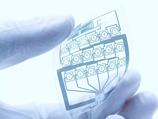
Peel-and-stick simplicity isn’t just for adhesive bandages any more. IoT and flexible hybrid electronics (FHE) are bound to change hardware business models. And flexible displays will breathe life into any surface.These were among the insights foreshadowing the future of the FHE, electronic textiles, IoT, MEMS and sensors industries at the FLEX Japan and MEMS Sensors Forum Japan 2018. At the April event, organized by SEMI-FlexTech-MSIG, nearly 200 attendees shared their observations and lessons learned in the development of processes, products and applications. Presentations and discussions revealed these five takeaways.1. Expect the unexpected with FHE developmentFlexible Hybrid Electronics (FHE) continues to shrink the size and weight of products, enabling new markets and concepts. “FHE takes printed electronics and adds ICs for getting performance out of the PE structure,” said Wilfried Bair of NextFlex, adding that “peel- and-stick electronic products are one example of unexpected new markets enabled by FHE capabilities.” One potential application is large peel-and-stick safety sensors adhered to buildings to warn of structural dangers.Another surprising turn: With new insights into OLED technology originally developed for flexible displays, Cambridge Display Technology (CDT) has devised an innovative medical diagnostic tool for markets such as biomedical and agricultural monitoring. The tool features an atmosphere-processable OLED component with a simplified OLED structure encapsulated in aluminum foil.2. IoT and FHE devices should change hardware business modelsThis is the standard business model for many new FHE products: develop a product, manufacture it, find customers and sell. FHE and IOT device developers were encouraged by Jam Kahn of Gemalto to consider flipping the script: During FHE product development, explore building an after-market revenue stream by controlling and mining the data for trends it reveals. Because of its data harvesting potential, IoT is an excellent emerging technology for this strategy.The “Experience Economy” could create 200 connectable items per person, generating strong revenue streams from the collection and analysis of massive amounts of sensor-generated data. The key is for the data to be actionable. That means hardware suppliers must extend their focus to software development. “A recent study of California investors found that by 2025, 60 percent of global business profits will be from data,“ noted Harri Kopola of VTT, who advised hardware producers to examine business models that produce continuous value by leveraging software. “With FHE, we are creating the path to digitization for non-digital industries, and these industries need complete solutions,” he said.Hardware provider Xenoma, for example, sells an electronic shirt with sensors for measuring muscle movements, heart rate and other health-related data. Xenoma’s Ichiro Amimori said the company offers its open-source software development kit for free under one condition: The developer must share the collection data with Xenoma. The idea is that the more data collected, the greater Xenoma’s ability to improve human health over the long term and achieve its long-term vision of alleviating disease.3. Roll-to-roll and sheet-to-sheet manufacturing will meet in the middleOne of the big advantages of flexible and printed electronics was its promise to enable the manufacturing of electronics on a roll-to-roll (R2R) process in atmospheric (or close) conditions, like newspaper, rather than one sheet at a time, as with displays or wafers. But as development of inks and interconnects progressed, along with the placement of discrete and thinned-die components and basic flexible substrates on a moving web, most research and development (R D) and limited-production runs moved to sheet-fed systems to control material costs for experiments and low-volume production. R D on printing electronics processes split into two camps: the simple printed components camp on R2R, and the camp backing more flexible hybrid electronics development on a sheet-by-sheet basis. But progress didn’t stop.Harri Kopola of VTT highlighted new R2R inspection and test capabilities in the VTT pilot line in Finland. R2R processing advances incorporate ideas from biology, chemistry, optics, optoelectronics, advanced inspection and test capability, illustrating the multidisciplinary nature of FHE. While accurate, high-speed, pick and place of thinned, bare die remains the domain of sheet-to-sheet manufacturing, look for more improvements in accuracy and speed.Another new manufacturing concept that turns business models on their heads – “minimal fabs” – focuses on creating limited-run equipment and processes that use 3D printing and do not require cleanrooms. With a relatively low cost of entry, the approach enables electronics to be produced affordably anywhere.4. Powering the IoT is a grand challengeThe requirement for edge devices to function without intervention for long periods raises hard questions about how to power the devices. Using organic photovoltaics (OPV) in textiles to harvest energy from light could be one solution, according to Kasimaesttro Sugino of the Suminoe Textile Technical Center. ULVAC’s answer to the IoT power issue are requirements for edge device micro-batteries to be environmentally benign, safe, flexible and compatible with semiconductor processing less than .1 mm in height. The micro-batteries must also feature a long life and support continuous power output, high power density, low self-discharge (over 10 years) and mass production, said Shunsuke Sasaki of ULVAC. The batteries are being built on silicon, glass and stainless steel with dry, thin-film vacuum processing. 5. Flexible displays bring any surface to lifeWith their durability, flexibility, low-cost processing and programmability, flexible displays can transform any surface into a content-rich display with messages that make lives healthier, simpler and safer.One example is FlexEnable’s organic thin-film transistor (OTFT), a device made possible not only by recent advances such as the ability to build organic material transistors on plastic and the increasing clarity of new film materials but by continuous manufacturing process improvements. These advances are improving switching times and the color and video capabilities of thin-film transistors while retaining their flexibility, low power consumption and communication capabilities. Simon Jone of FlexEnable gave the examples of wrapping a display around the blind spots of automobiles or replacing side-view mirrors with interior monitors showing feeds from an external camera, approaches that would improve safety while reducing wind drag and increasing fuel efficiency.E Ink’s reflective technology and flexible products are coming to market with a wider color spectrum. The company’s Michael McCreary said its designers are specifying the panels for innovative projects such as the exterior walls of the San Diego International Airport parking garage. Used to communicate with airport visitors, the installation is weather-proof, programmable and self-powered.
Read More
Enjoying the richest lineup of talent and resources in SEMI history, West isn’t just a show anymoreIt’s a powerful conversation. With new venues, new voices, and new takes on the industries and markets that will fuel the industry’s growth, SEMICON West is adding more value and taking a fresh approach to event experiences.Arrive smart, advance to “beyond smart.” That’s AI we’re talking about, and you’ll see demos on how it’ll enhance every one of our established and emerging markets. TechXPOT pavilions will be ground zero for discussing the freshest perspectives about autonomous and connected transportation and smart manufacturing. Designed exclusively to increase your expertise in the most promising areas for the next five years of industry growth, the featured interactions will center around innovations for improving data sharing across the global supply chain.Meet the experts. They’ll be waiting for you at the Meet the Experts Theater in the Smart Manufacturing and Smart Transportation Pavilions located on the show floor. Placed specifically for your easy access, the experts represent the top of their fields in emerging IC technologies for leveraging connected intelligence in electronics manufacturing. They’ll drive conversations about the hottest areas of growth opportunity and how to crack the challenges facing the industry. They look forward to the specifics that you want to explore. “Workforce development” has become a rallying cry. Coming off a banner year, the chip business is mounting an unprecedented recruitment drive to attract the best talent. The results are vital for the next state-of-the-art tech roadmaps that rely on the most intelligent minds. To help accelerate learning curves, the Smart Workforce Pavilion welcomes college students and recent grads to see the engineering pros discuss what it’s like to work in the microelectronics industry, and to gain an understanding about what technologies will be driving the future.As an engineer and executive, I’ve attended SEMICON West for 25 years – this year’s event raises to another level the value of content and networking for all. Let’s talk at the show. We want to hear your ideas about how we move beyond smart to even higher growth and innovation.Register today for an Expo Pass to tour the exhibition floor and gain access to the Smart Pavilions and Meet the Experts Theaters. Or choose the Thought Leadership or All-in Pass to receive access to the TechXPOT presentations and more. To view all conference pass benefits, visit www.semiconwest.org/pricing.Great products start with semiconductors. Conversations make them happen.
Read More