downloadGroupGroupnoun_press release_995423_000000 copyGroupnoun_Feed_96767_000000Group 19noun_pictures_1817522_000000Member company iconResource item iconStore item iconGroup 19Group 19noun_Photo_2085192_000000 Copynoun_presentation_2096081_000000Group 19Group Copy 7noun_webinar_692730_000000Path
Skip to main content
Default Banner Image

imec

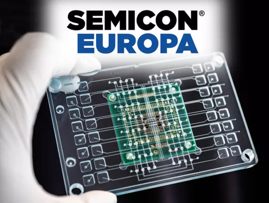
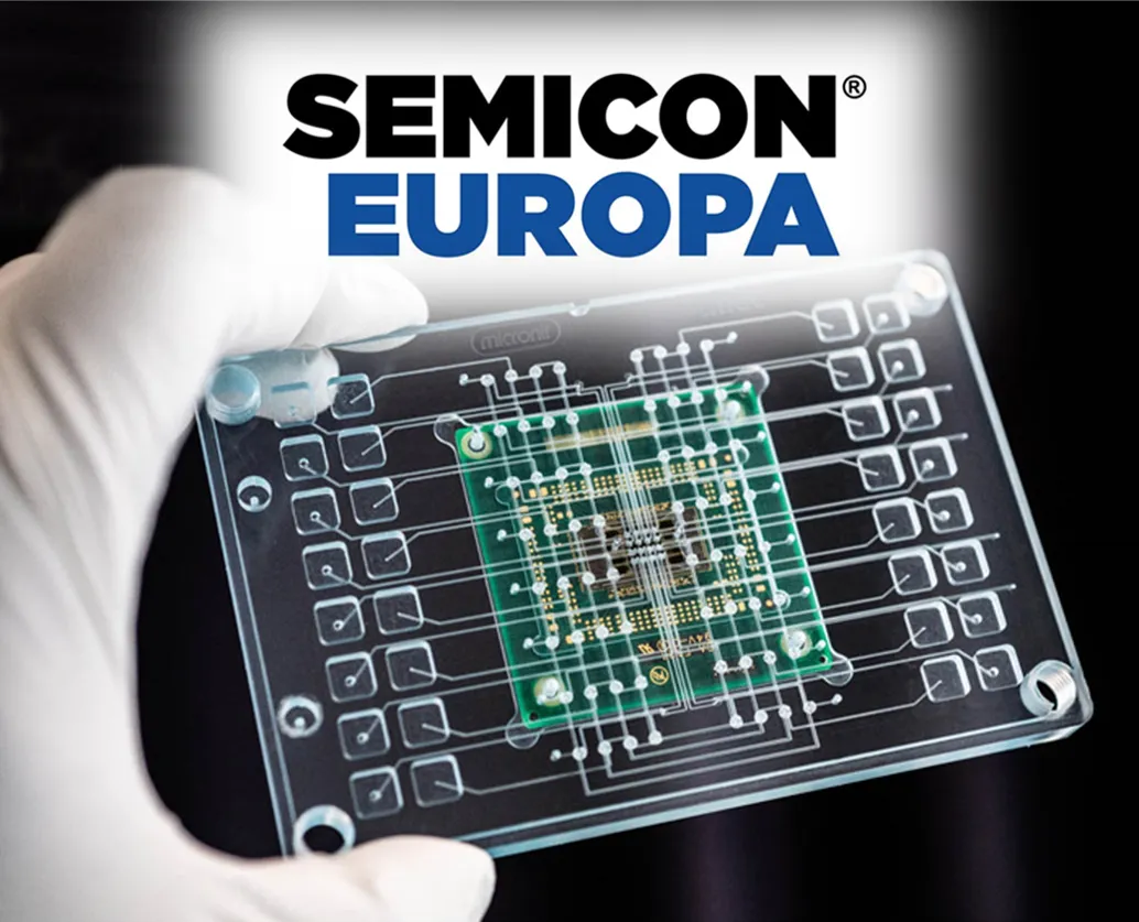
Healthcare has traditionally focused on one-size fits-all medication to treat populations instead of tailoring treatments to individual patients. Recent advances in stem cell technology allow researchers to create disease models for personalized medicine. SEMI spoke with Thomas Pauwelyn, Postdoctoral Researcher at imec, about trends in medical technology innovation such as organ-on-chip devices and their applications. Pauwelyn shared his views ahead of his presentation at the SEMI SMART MedTech Forum, 13-14 November, in Hall B2 (Inspiration Hub) at SEMICON Europa, 12-15 November, 2019, in Munich, Germany. Join us at the event to meet experts from imec.xpand and other key industry influencers. Registration is open. Participation is free of charge for SEMICON Europa visitors. SEMI: What triggered the healthcare move from a one-size fits-all medication to treat populations to tailored treatments? What advancements allowed researchers to create models for personalized medicine? Pauwelyn: One of the main triggers for this transition is the inefficiency of the current healthcare system. The top 10 highest grossing drugs in the U.S. are effective for only between 1 in 25 to 1 in 4 patients. Not only do most medicines only help a small share of the patients, but they are often developed in classical clinical trials with predominantly western or male participants.Recent advances in stem cell technology allow researchers to create disease models for individual patients. In other words, researchers can reprogram cells from a patient’s skin or blood sample to various cell types, including cardiac or neuronal cells, through stem cell techniques. These samples reflect the traits that make a patient unique.However, patient-in-a-dish models expose cells to very artificial environments. So these models look very different from their counterparts in the body. Organ-on-chip systems address these issues by exposing cells to physiologically relevant conditions and create more mature models. SEMI: What is exactly an organ-on-chip? Pauwelyn: Organ-on-chip devices are microfluidic cell culture chips that can revolutionize the development of drugs and personalized treatments. These devices model the pathophysiological behavior of organs and tissues. Inside these chips, cell cultures are grown and exposed to conditions that better resemble in vivo microenvironment. Different organ models can be created by exposing different cell types to an engineered microenvironment. Common examples are the heart-on-chip, lung-on-chip, gut-on-chip or brain-on-chip.SEMI: Medical technology has made astonishing advances over the years. As new medical devices emerge, what are the main challenges?Pauwelyn: Meeting stringent regulatory requirements is one of the main challenges for medical devices. Technologies related to personalized medicine do not neatly fit in existing health technology assessments and reimbursement processes.In the case of organ-on-chip devices, there are challenges related to production, qualification and adoption. Increased standardization will also help scientists compare and interpret their findings. Currently, various research groups obtain different results from own organ-on-chip systems. These systems may be fabricated from different or exotic materials, expose cells to different microenvironments or rely on other cell models. Often, only a few devices are available for testing due to limited fabrication scalability.SEMI: What did imec do to overcome those challenges?Pauwelyn: imec turned to its expertise in chip design and technology to develop a novel organ-on-chip platform in close collaboration with Micronit Microtechnologies in the InForMed project funded by the ECSEL Joint Undertaking (ECSEL2014-2-662155). The platform’s main requirements were that it could reduce handling variability by microfluidic automation, be fabricated with conventional materials compatible with production upscaling, and produce high-quality electrical recordings of cellular activity. Another essential requirement was the compatibility of the device to the standard workflow of pharmaceutical research. The user interface is based a conventional 96-well plate, and peristaltic pumps are integrated into the device.SEMI: How does the CMOS-based microelectrode array work and where do you see potential for applications in the field of personalized medicine?The imec-developed CMOS-based microelectrode array is the sensor in our organ-on-chip system that monitors the cell culture. The sensor consists of 16,384 electrodes distributed over 16 independent microfluidic wells. It detects cellular activity down to the single-cell level, including intracellular action potentials or extracellular signals from electrically active cells or impedance caused by cells growing directly over the electrode.We believe this technology has great potential for developing miniaturized patient models in the lab. By using patient cells reprogrammed to the desired cell types through stem cell technologies, we can develop patient-on-chip systems. These systems would be able to predict which treatment is best suited for a specific patient or how drugs affect certain subpopulations.SEMI: What are your expectations for the SMART MedTech Forum at SEMICON Europa 2019 in Munich? Pauwelyn: The SMART MedTech Forum brings together an interesting mixture of researchers, entrepreneurs and stakeholders in the future of healthcare. I look forward to hearing their perspectives and to discuss how personalized medicine and MedTech will help tackle current challenges.SEMI: Can you share one prediction for the future of MedTech? Pauwelyn: I believe that MedTech in the future will help us tailor treatments to each patient. Doctors will have a wide arsenal of tools available to predict which treatment will deliver both the highest chance of success and the lowest chance of adverse reactions. One of these tools could be a human-patient-on-chip system. It would consist of interlinked organ-on-chip modules with patient-derived cell models. In this way, the reaction of patients to specific treatments could be predicted without ever exposing them to potentially harmful compounds.Dr. Thomas Pauwelyn currently is a post-doctoral researcher with an Innovation Mandate grant from VLAIO, investigating strategies to valorize the results from his research. Pauwelyn’s research focuses on developing novel organ-on-chip systems for predictive toxicology and drug development. He also investigates how organ-on-chip devices may help stratify patients and help enable personalized medicine. Pauwelyn has studied at KU Leuven, Belgium, since 2008. He earned his BSc in Bioscience Engineering specializing in Catalytic Technologies in 2011 and a Master’s in Nanoscience and Nanotechnology with the Bioscience Engineering option in 2013. He completed an IWT fellowship for a PhD at KU Leuven and imec’s Life Science Technologies group in 2018.Serena Brischetto is senior manager, marketing and communications, at SEMI Europe.
Read More
Last year the industry posted another remarkable double-digit revenue growth year. IC shipments eclipsed one trillion units for the first time and continued to enable an ever-expanding array of silicon intensive-applications.2018 was also a pivotal year of transformation at SEMI. Setting our sights firmly on building more value for SEMI members, we doubled down on priorities I established this time last year. We advocated intensively on global trade policies, industry talent needs, and critical environment, health and safety (EHS) concerns. To underpin our efforts around talent, we took the bold step to reinvigorate the industry’s identity with a dynamic image campaign. Above all, we targeted critical industry-wide issues to help us realize the ambition of becoming a trillion-dollar industry in the next decade. Workforce DevelopmentRedefining our approach to talent development in 2018 was and remains a top priority. A diverse, highly skilled workforce is crucial to the industry’s ability to innovate. Last year we ramped up a number of SEMI High Tech U (HTU) programs to inspire young people and attract them to careers in high-tech manufacturing. To date, more than 130,000 students have been touched by HTU – through student or teacher programs.Over the past year, we designed a new university outreach program and established partnerships with 100 institutions. We established Workforce Pavilions at SEMICON events in Southeast Asia, the U.S., Taiwan, Europe and Japan for students to explore career opportunities and meet with recruiters. We thrilled at seeing sponsors hire young talent at SEMI events. This year, all SEMICONs worldwide will feature Workforce Pavilions.SEMI also formalized its commitment to Diversity and Inclusion (D I) with the establishment of a D I council to shape new programs including the recently launched Spotlight on SEMI Women. To localize and fully optimize our D I programs, we established regional workforce councils in every region we serve. We unveiled the SEMI Mentoring Program to support students and young professionals on this journey by facilitating one-on-one mentoring relationships with industry professionals. Hundreds of mentees have enrolled. But we still need more mentors. I urge you to join the program. During the year, SEMI also expanded its workforce staff and developed a comprehensive workforce strategy with programs that engage students as early as elementary school and inspires them through high school and college. The program provides pathways to professional careers, building a pipeline to fill the short-term and long-term talent needs of the industry. Industry Image CampaignAs we developed the comprehensive workforce development program, we knew we had to refresh the industry’s image and appeal to the next generation through contemporary media and communications channels. So we recently launched a bold, innovative campaign to raise industry awareness and attract students and recent graduates to careers in semiconductor manufacturing.Our You’re Welcome campaign is a novel, creative approach that blends entertainment, media and storytelling to excite students about the industry. The campaign went viral immediately and within weeks had more than 5.5 million social media impressions and 2.3 million video views.Trade Policy AdvocacyRising trade tensions between the U.S. and China catapulted global trade policy to the forefront of industry concerns in 2018. Since the tariffs have taken force, semiconductor companies have faced higher costs, greater uncertainty, and difficulty selling products abroad. The tariffs have forced many SEMI member companies to pause or rethink their investment strategies.SEMI quickly engaged U.S. policymakers and provided resources for SEMI members. We formed a member trade task force, staged trade compliance seminars in China, and convened meetings with over 110 U.S. congressional, agency and administration officials, and provided testimony on the importance of the free trade to the industry.SEMI continues to educate policymakers about the critical importance of free and fair trade, open markets, and respect and enforcement of IP for all players in the global electronics manufacturing supply chain. As part of this initiative, we distributed “10 Principles for the Global Semiconductor Supply Chain in Modern Trade Agreements” and encouraged their adoption in various trade negotiations. These principles outline the primary considerations for balanced trade rules that benefit SEMI members around the world, strengthen innovation and perpetuate the societal benefits of affordable microelectronics.Environment, Health and SafetyEnvironmental regulations are proliferating globally even as advanced semiconductor manufacturing technology relies increasingly on a host of new materials. With dozens of new fabs and fab line upgrades, our industry must align on best practices, sensibly respond to materials restrictions, and renew efforts toward sustainable manufacturing.That’s why the revitalization of SEMI EHS efforts became another priority in 2018. Two months ago, we hosted the inaugural EHS Summit at SEMI Headquarters. Fully, 70 EHS professionals and company executives met to form the basis for the future SEMI EHS program.The Year AheadDespite a softening in the market, compounded by Apple’s first-ever announcement of a revenue decline in 16 years, a geopolitical whirlwind on trade and an extended shutdown of much of the U.S. government, the future is bright.At SEMI’s annual Industry Strategy Symposium (ISS 2019) in Half Moon Bay, Calif. in early January, the sense of optimism was palpable. In her keynote address, Dr. Ann Kelleher, Sr. VP and General Manager, Technology and Manufacturing Group, at Intel, observed that data is powering the fourth industry revolution and the expansion of compute. With customers expecting continual improvements in applications, Kelleher highlighted the tremendous opportunity for the chip industry to meet these expectations.At ISS 2019, we announced a Memorandum of Understand between SEMI and imec. The MOU will enable us to accelerate our members’ engagement in SEMI’s Smart vertical market platforms, in particular Smart MedTech and Smart Transportation. Our partnership with imec will also allow us to boost SEMI Standards activities in non-CMOS technologies, deepen technology roadmap efforts and augment our SEMI Think Tank initiative in thought leadership at a global level.Over the course of this coming year, will we begin our global rollout of key building blocks of our comprehensive workforce development program to engage schoolchildren as young as 10 and learners all the way to veterans who return to the workforce. We are now able, with the invaluable help of our Workforce Development Council and the passionate engagement of many SEMI member companies, to offer a solution to the talent crisis in our industry.We will continue to be the leading voice for our members and the end-to-end semiconductor supply chain across Talent, Trade, Tax and Technology as we work to ensure free, fair trade that protects IP while preserving vital access to markets to grow the supply chain. Vertical Market PlatformsOur vertical market platforms are an important part of this growth. For example, in Smart MedTech, SEMI looks forward to working with the Nano-Bio Materials Consortium to advance human monitoring technology for telemedicine and digital health after winning $7 million to fund the renewed program. In Smart Transportation, we will leverage the Global Automotive Advisory Council (GAAC) we formed last year to represent the full automotive supply chain and the Smart Transportation and Smart Automotive forums featured at all our SEMICON events to enable the industry to identify and seize opportunities in autonomous driving. At ISS 2019, Sujeet Chand of Rockwell Automation noted that “digitization will grow faster in the next 10 years than it did in the past 50,” a trend calling for semiconductor fab architectures that transform data into business value. We will continue to bring the industry together at our Smart Manufacturing venues to help uncover ways to deploy deep learning, edge computing and other Smart technologies to deliver this value and meet the challenges of automation as artificial intelligence’s (AI) sprawling influence reshapes industries including manufacturing.I am filled with optimism and thrilled about the opportunities I see on the horizon for our members as we build on our 2018 accomplishments to enable your prosperity in 2019 and beyond. My heartfelt thanks to all of you for your participation in our programs and events.I look forward to another successful year as we connect, collaborate and innovate together!Ajit Manocha is president and CEO of SEMI.
Read More
The Scaling Technologies TechXPOT at this year’s SEMICON West (Scaling Every Which Way! – Thursday, July 12, 2:00pm-4:00pm) will explore traditional scaling as the industry marches toward 3nm and beyond, as well as technologies that enable 3D architectures, die stacking, and interconnect scaling. The session will also provide an update on how the various players (foundry, IDM, fabless, and application developers) are jockeying for innovation leadership. As a prelude to the event, SEMI asked Priya Mukundhan, director, Technology Development and Applications, at Rudolph Technologies, and a speaker at the TechXPOT, to provide her insights into challenges associated with metrology and inspection.For a full list of speakers and program agenda, visit http://www.semiconwest.org/programs-catalog/scaling-every-which-way. Priya Mukundhan, director, Technology Development and Applications, Rudolph TechnologiesSEMI: What are the key challenges that need to be addressed to provide the kind of metrology and inspection solutions that will be needed by the industry as scaling – in all its forms (e.g., traditional, 3D ICs, interconnect, and different transistor architectures) – is pursued at 5nm and then at 3nm? Priya Mukundhan: With respect to metrology needed to scale FinFETs, the following will be key: Gate critical dimension (CD) at the fin sidewall, gate height, gate profile Fin CD, height and profile Dopant profiles Stress measurement in the fin Composition in thin film and interface These challenges are currently being handled using in-line CD solutions, CD scanning electron microscopy (CD-SEM) and CD atomic force microscopy (CD-AFM), along with optical critical dimension (OCD) measurements. There is no single technology that can take all of these measurements, and determining the right solution is application-dependent[1].Issues associated with inspection and scaling include the following: Bright-field inspection lacks the sensitivity to detect defects smaller than those found at the 20nm node Detecting defects that are 5nm or smaller is achieved using electron beam inspection tools, but these single-electron beam inspection systems are prohibitively slow and cannot meet the high-volume manufacturing (HVM) requirements for defect inspection Buried defects Void detection in 3D SiP structures, front and backside inspection Sidewall crack detection in packaging SEMI: Can you provide a summary of the R D roadmap for metrology/inspection tools that you see emerging in order to get to 3nm? PM: Hybrid metrology is currently in use, especially for CD metrology. To support the development efforts, techniques that provide complementary information as well as those that eliminate uncertainties will be required. Researchers at imec[2] have started exploring technology combinations to gain insight into how new structures function. Some of the findings in imec’s study include the following: The combination of transmission electron microscopy (TEM) and scanning probe microscopy (SPM) provides a unique approach of imaging combined with a functional analysis capability In situ SPM could potentially determine composition (SIMS) as well as functional properties (electrical) Fast Fourier transform scanning spreading resistance microscopy (FFT-SSRM) is a novel technique that measures carrier profiles in semiconductors. This overcomes the current SSRM limitations of signal distortions due to parasitic resistances while measuring on small volumes such as FinFET and nanowires Multi-electron beam inspection can be used for HVM for sensitivity to smaller SEMI: How will metrology and inspection be impacted beyond 3nm? What kinds of tools will be needed by that point in time?PM: There are several different transistor options that have been identified by leading edge wafer fabs and consortia looking beyond the 5nm node roadmap[3,4]. Some of the options on the table include the following: 1) Extension of the current FinFET in the form of gate-all-around FET2) Creating them with new materials by adding ferroelectrics (e.g., negative capacitance FET, or NC-FET) 3) Complementary FET4) Vertical nanowires and nanosheet FETsThese possibilities bring new challenges and require characterization at the material level. Also, the industry as a whole will have to redefine what it means to do composition at the nanometer level. This could be the beginning of a trend towards array-based metrology, i.e., measurements on an array of devices to gather statistically significant data[2].Regarding metrology needs at 3nm, it is too early to determine what kind of tools would be needed only for R D and how many of them would need to be extended to high-volume manufacturing (HVM). From an inspection perspective, there will be a continued migration towards computer aided design (CAD)-based inspection, as well as having the ability to deal with large image data sets (petabyte, big data). Furthermore, inspection algorithms should be improved, along with better staging for better image stitching.References Bunday, E. Solecky, A. Vaid, A. F. Bello, X. Dai, “Metrology capabilities and needs for 7nm and 5nm logic nodes,” Proc. Of SPIE, Vol. 10145, 101450G, pp. 1-41, 2017. Imec roadmap and imec magazine. Intel roadmap. https://semiengineering.com/transistor-options-beyond-3nm/ Debra Vogler, SEMI
Read More