downloadGroupGroupnoun_press release_995423_000000 copyGroupnoun_Feed_96767_000000Group 19noun_pictures_1817522_000000Member company iconResource item iconStore item iconGroup 19Group 19noun_Photo_2085192_000000 Copynoun_presentation_2096081_000000Group 19Group Copy 7noun_webinar_692730_000000Path
Skip to main content
Default Banner Image

Environment

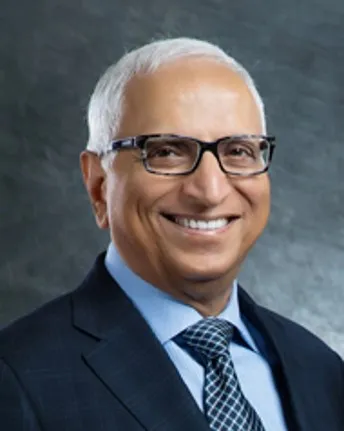
Last year the industry posted another remarkable double-digit revenue growth year. IC shipments eclipsed one trillion units for the first time and continued to enable an ever-expanding array of silicon intensive-applications.2018 was also a pivotal year of transformation at SEMI. Setting our sights firmly on building more value for SEMI members, we doubled down on priorities I established this time last year. We advocated intensively on global trade policies, industry talent needs, and critical environment, health and safety (EHS) concerns. To underpin our efforts around talent, we took the bold step to reinvigorate the industry’s identity with a dynamic image campaign. Above all, we targeted critical industry-wide issues to help us realize the ambition of becoming a trillion-dollar industry in the next decade. Workforce DevelopmentRedefining our approach to talent development in 2018 was and remains a top priority. A diverse, highly skilled workforce is crucial to the industry’s ability to innovate. Last year we ramped up a number of SEMI High Tech U (HTU) programs to inspire young people and attract them to careers in high-tech manufacturing. To date, more than 130,000 students have been touched by HTU – through student or teacher programs.Over the past year, we designed a new university outreach program and established partnerships with 100 institutions. We established Workforce Pavilions at SEMICON events in Southeast Asia, the U.S., Taiwan, Europe and Japan for students to explore career opportunities and meet with recruiters. We thrilled at seeing sponsors hire young talent at SEMI events. This year, all SEMICONs worldwide will feature Workforce Pavilions.SEMI also formalized its commitment to Diversity and Inclusion (D I) with the establishment of a D I council to shape new programs including the recently launched Spotlight on SEMI Women. To localize and fully optimize our D I programs, we established regional workforce councils in every region we serve. We unveiled the SEMI Mentoring Program to support students and young professionals on this journey by facilitating one-on-one mentoring relationships with industry professionals. Hundreds of mentees have enrolled. But we still need more mentors. I urge you to join the program. During the year, SEMI also expanded its workforce staff and developed a comprehensive workforce strategy with programs that engage students as early as elementary school and inspires them through high school and college. The program provides pathways to professional careers, building a pipeline to fill the short-term and long-term talent needs of the industry. Industry Image CampaignAs we developed the comprehensive workforce development program, we knew we had to refresh the industry’s image and appeal to the next generation through contemporary media and communications channels. So we recently launched a bold, innovative campaign to raise industry awareness and attract students and recent graduates to careers in semiconductor manufacturing.Our You’re Welcome campaign is a novel, creative approach that blends entertainment, media and storytelling to excite students about the industry. The campaign went viral immediately and within weeks had more than 5.5 million social media impressions and 2.3 million video views.Trade Policy AdvocacyRising trade tensions between the U.S. and China catapulted global trade policy to the forefront of industry concerns in 2018. Since the tariffs have taken force, semiconductor companies have faced higher costs, greater uncertainty, and difficulty selling products abroad. The tariffs have forced many SEMI member companies to pause or rethink their investment strategies.SEMI quickly engaged U.S. policymakers and provided resources for SEMI members. We formed a member trade task force, staged trade compliance seminars in China, and convened meetings with over 110 U.S. congressional, agency and administration officials, and provided testimony on the importance of the free trade to the industry.SEMI continues to educate policymakers about the critical importance of free and fair trade, open markets, and respect and enforcement of IP for all players in the global electronics manufacturing supply chain. As part of this initiative, we distributed “10 Principles for the Global Semiconductor Supply Chain in Modern Trade Agreements” and encouraged their adoption in various trade negotiations. These principles outline the primary considerations for balanced trade rules that benefit SEMI members around the world, strengthen innovation and perpetuate the societal benefits of affordable microelectronics.Environment, Health and SafetyEnvironmental regulations are proliferating globally even as advanced semiconductor manufacturing technology relies increasingly on a host of new materials. With dozens of new fabs and fab line upgrades, our industry must align on best practices, sensibly respond to materials restrictions, and renew efforts toward sustainable manufacturing.That’s why the revitalization of SEMI EHS efforts became another priority in 2018. Two months ago, we hosted the inaugural EHS Summit at SEMI Headquarters. Fully, 70 EHS professionals and company executives met to form the basis for the future SEMI EHS program.The Year AheadDespite a softening in the market, compounded by Apple’s first-ever announcement of a revenue decline in 16 years, a geopolitical whirlwind on trade and an extended shutdown of much of the U.S. government, the future is bright.At SEMI’s annual Industry Strategy Symposium (ISS 2019) in Half Moon Bay, Calif. in early January, the sense of optimism was palpable. In her keynote address, Dr. Ann Kelleher, Sr. VP and General Manager, Technology and Manufacturing Group, at Intel, observed that data is powering the fourth industry revolution and the expansion of compute. With customers expecting continual improvements in applications, Kelleher highlighted the tremendous opportunity for the chip industry to meet these expectations.At ISS 2019, we announced a Memorandum of Understand between SEMI and imec. The MOU will enable us to accelerate our members’ engagement in SEMI’s Smart vertical market platforms, in particular Smart MedTech and Smart Transportation. Our partnership with imec will also allow us to boost SEMI Standards activities in non-CMOS technologies, deepen technology roadmap efforts and augment our SEMI Think Tank initiative in thought leadership at a global level.Over the course of this coming year, will we begin our global rollout of key building blocks of our comprehensive workforce development program to engage schoolchildren as young as 10 and learners all the way to veterans who return to the workforce. We are now able, with the invaluable help of our Workforce Development Council and the passionate engagement of many SEMI member companies, to offer a solution to the talent crisis in our industry.We will continue to be the leading voice for our members and the end-to-end semiconductor supply chain across Talent, Trade, Tax and Technology as we work to ensure free, fair trade that protects IP while preserving vital access to markets to grow the supply chain. Vertical Market PlatformsOur vertical market platforms are an important part of this growth. For example, in Smart MedTech, SEMI looks forward to working with the Nano-Bio Materials Consortium to advance human monitoring technology for telemedicine and digital health after winning $7 million to fund the renewed program. In Smart Transportation, we will leverage the Global Automotive Advisory Council (GAAC) we formed last year to represent the full automotive supply chain and the Smart Transportation and Smart Automotive forums featured at all our SEMICON events to enable the industry to identify and seize opportunities in autonomous driving. At ISS 2019, Sujeet Chand of Rockwell Automation noted that “digitization will grow faster in the next 10 years than it did in the past 50,” a trend calling for semiconductor fab architectures that transform data into business value. We will continue to bring the industry together at our Smart Manufacturing venues to help uncover ways to deploy deep learning, edge computing and other Smart technologies to deliver this value and meet the challenges of automation as artificial intelligence’s (AI) sprawling influence reshapes industries including manufacturing.I am filled with optimism and thrilled about the opportunities I see on the horizon for our members as we build on our 2018 accomplishments to enable your prosperity in 2019 and beyond. My heartfelt thanks to all of you for your participation in our programs and events.I look forward to another successful year as we connect, collaborate and innovate together!Ajit Manocha is president and CEO of SEMI.
Read More
Environmentally sound policies and the health and the safety of workers in the microelectronics supply chain are vitally important to SEMI and its members. For more than two decades, together we have focused on worker safety by focusing on global environment, health and safety (EHS) compliance and regulatory issues and the advancement of sound EHS practices. Today, EHS has taken on an even higher profile in the microelectronics industry with its growth across Europe, North America and Asia. Never has the industry been under greater scrutiny. The list of regulatory agencies is growing. To keep pace with rising EHS requirements and continue to ensure worker safety, we’d like your help. The SEMI EHS summit will open with a keynote presentation from Russ LaMotte, Managing Principal of Beveridge Diamond, and a recognized expert on EHS issues in the electronics industry. Member companies representing equipment, materials, facilities and devices will then each share their EHS concerns. Finally, working groups will address industry EHS challenges and gaps. Outputs from the working group meetings will form the basis for the future SEMI EHS program. The EHS issues SEMI’s program and company volunteers are addressing include: PFOA – Government efforts to eliminate pefluoro-octanoic acid and related compounds and salts (collectively known as PFOA) from company supply chains REACH – A European Union regulation to strengthen protections against chemical risks to human health and the environment. Other countries – Japan, Korea, Taiwan – have enacted similar regulations. Stockholm Convention – An international environmental treaty designed to eliminate or restrict the production and use of persistent organic pollutants (POPs) Waste Framework Directive Database – The European Commission and the European Chemicals Agency (ECHA) are building a database where all suppliers will be required to register certain articles. Other groups are dealing with country-specific aspects of the Restriction of Hazardous Substances (RoHS) and the Toxic Substances Control Act (TSCA). Complementing our advocacy efforts, SEMI has established 25 primary EHS standards with SEMI S2 (Safety) as the cornerstone. The S2 family of SEMI Standards acts as performance-based EHS considerations for semiconductor manufacturing equipment and has also been adopted by adjacent industries. Sign up for the November 29th SEMI EHS Summit today Team up with your SEMI colleagues to collectively formulate the semiconductor manufacturing industry’s EHS program. SEMI members can register for the November 29th SEMI EHS Summit by clicking here. If you cannot make this meeting but wish to be added to SEMI’s regular communication on EHS and Advocacy issues, please click here and choose Advocacy from the list of topic choices. Michael Ciesinski is vice president of the FlexTech Alliance, a SEMI Strategic Association Partner chartered with building up infrastructure for flexible electronics manufacturing.
Read More
IntroductionStarting July 4, 2022, PFOA (Perfluorooctanoic acid) levels in semiconductor manufacturing and related equipment (SMRE), including replacement parts, entering the European Union (EU) will be restricted to 25 ppb per component (or any part thereof). Semiconductor equipment components (and the parts thereof) of particular concern include fluid tubing and fittings, pipe/seal tape, wire and cable insulation, filters, valves, tanks, panels, reaction vessels and o-rings; if they are made from fluoropolymers or fluoroelastomers.When PFOA is used as an aid to the manufacture fluoropolymers such as PTFE, PFA, PVDF or fluoroelastomers such as FKM and FFKM (collectively referred to as fluoromaterials), an unintended PFOA residue can be trapped within the fluoromaterial. Buyers of components used in SMRE are usually unaware of the processing method used for any fluoromaterials they may contain, and, as a consequence, the potential for PFOA residue. This lack of information about potential PFOA residues could result in regulatory enforcement actions and restricted market access, particularly in the EU.The impact of restrictions on fluoromaterials used in SMRE has been introduced in previous SEMI articles ‘Fluorinated Compound Restrictions May Trigger Costly Equipment Changes’ and ‘Fluorinated Substance Restrictions Triggers Costly Equipment Changes.’PFOA and its related compounds, such as the ammonium salt APFO (collectively called PFOA in this article), are recognized internationally as hazardous chemicals and are now targeted for regulatory restriction in the U.S., Taiwan, Canada and the EU. The UN Stockholm Convention on Persistent Organic Pollutants (POPs) is also considering listing PFOA, which could lead to additional international restrictions.The SEMI EHS Division PFOA Compliance Working Group has been working to understand: The likelihood of PFOA residue entering the supply chain of new components The residual level of PFOA in fluoromaterials produced prior to the phase out of PFOA by some manufacturers The impact of PFOA residue on the secondary equipment market This SEMI resource page, ‘Elimination of PFOA from the Equipment Supply Chain,’ and the supporting FAQ contain the Working Group’s key findings and conclusions.PFOA in the Fluoromaterial Supply ChainSignatories to the U.S. EPA Stewardship Program, which include FluoroCouncil members, eliminated PFOA from their manufacturing processes by 2013. However, other fluoromaterial manufactures – particularly in China, Russia and India – might still use PFOA and pose a significant risk to the worldwide supply chain.China, the world’s largest fluoromaterial producer, accounts for 53 percent of global production of PTFE and 38 percent of worldwide production of PVDF, FEP and FKM. An estimated 75 percent to 85 percent of fluoromaterials are manufactured using PFOA in China. Fully 25 percent of these fluoromaterials are exported, primarily to the U.S, Japan, EU and India. What’s more, finished goods made from or containing fluoromaterials that might be used as components in SMRE are exported from China.Documentation that traces fluoromaterials through the supply chain back to the original fluoromaterial manufacturer is key to meeting the PFOA regulatory requirements. This traceability can be straightforward in cases when an SMRE manufacturer directly specifies the use of a fluoromaterial in a custom-fabricated fluoromaterial component. However, for off-the-shelf components (e.g., cable ties, wiring insulation, tubing) or the components assembled from these components (e.g., controllers), the complexity and dynamics of the supply chain makes traceability back to the original fluoromaterial producer almost impossible.Residual PFOA Levels If, or how much, PFOA/APFO residue is contained in a fluoromaterial depends on the manufacturing process. Details of the manufacturing processes are proprietary and vary widely. Post manufacturing thermal treatments, such as sintering, extrusion, and molding, can result in the rapid thermal decomposition of APFO above 250C, but PFOA is significantly more stable. The temperature and time of thermal treatments is also proprietary and varies depending on the type of fluoromaterial and what is being made.This variability makes it impossible to estimate the likely level of trapped PFOA or APFO in a finished component or a part thereof. It is unwise to use data on the level of residue made known for one case to extrapolate the level of residue across the fluoromaterial industry. However, an industry-wide range on the order of 1ppm-10ppm (nearly 1000 times the EU limit) is suspected. Testing for the presence of PFOA/APFO at 25ppb in components is also problematic as there is no standard test method, and results among the custom methods developed in each test lab may vary.Given this uncertainty in test methods, a system of supplier declarations warrants consideration.Impact on Secondary (Used) EquipmentThe EU REACH restrictions apply to SMRE and replacement parts placed on the market at any time (not just initial placement – known as “first placing on the market”). For fluoromaterial components manufactured prior to 2013, there is a higher likelihood of residual PFOA/APFO levels exceeding the 25ppb limit of EU REACH. In principle all the SMRE components containing fluoromaterials should be investigated, and those containing PFOA above 25ppb must be replaced before the SMRE can be legally placed again on the EU market. Companies (e.g., semiconductor manufacturers) in the EU who wish to sell used equipment within the EU will be required to demonstrate the used equipment is in compliance. Selling older used equipment would likely be unprofitable after necessary investigations and component replacements are completed.Next StepsWhile the EU semiconductor manufacturing industry heavily depends on the secondary (used) equipment market, EU regulators may be unaware of the PFOA restriction’s damaging impact to this market. The EHS Division PFOA Working Group, in conjunction with SEMI Europe, is now considering how to bring this concern to the attention of regulators and to collaborate and lobby for effective changes including possible modifications to the EU Persistent Organic Pollutants (POPs) regulation.
Read More