downloadGroupGroupnoun_press release_995423_000000 copyGroupnoun_Feed_96767_000000Group 19noun_pictures_1817522_000000Member company iconResource item iconStore item iconGroup 19Group 19noun_Photo_2085192_000000 Copynoun_presentation_2096081_000000Group 19Group Copy 7noun_webinar_692730_000000Path
Skip to main content
Default Banner Image

AI

The SEMICON West 2025 design program “The Convergence of Semiconductor Manufacturing and Design,” organized by the ESD Alliance (ESDA), a SEMI Technology Community, featured presentations about successful collaborations between the design and manufacturing markets. The three-hour program in a packed conference room included plenty of great material that we’re using as the basis for a blog series that you will see over the next several months. I’m working on them now based on my conversations with four of the speakers where we discuss key drivers behind the need for collaboration and what’s ahead.I’m starting with Dave Kelf, CEO of Breker Verification Systems, a company steeped in front-end chip verification, who describes an actual circular collaboration that effectively leverages AI and other electronic design automation (EDA) advances. We recently talked about collaboration, integrated design and manufacturing flows and AI.Smith: How does Breker define collaboration between design and manufacturing? Kelf: In general, at a technical level, we would define this collaboration as the sharing of data, methodology and/or information that improves both processes. As semiconductors become more complex, this sharing process is increasingly important to effectively manage the overall complexity of today’s chip designs.Smith: What trends are driving the need for this collaboration?Kelf: Apart from the ever-increasing size and density of semiconductors, there are specific trends that require more interaction between design, verification and manufacturing. Obvious developments include the advent of chiplets, given the changes in performance of signal paths, and 3D devices driving complex packaging, power dissipation and other issues. Design issues such as the increased need for SoC coherency testing and complex device structures such as multi-core processors, also play a role. With many of these issues, design and verification (D/V) trade-offs have an impact on manufacturing, and vice versa. For example, differing delays on a Universal Chiplet Interconnect Express (UCIe) interface—an open specification for a die-to-die interconnect and serial bus between chiplets—will have an impact on hazard testing in coherency verification. As another example, thermal hotspots on some parts of a chip package might need additional testing during the verification phase. Smith: What trends and challenges are preventing a fully integrated design and manufacturing design flow?Kelf: Traditionally, the D/V and manufacturing teams have remained separate in most organizations, as well as between the two industries. EDA companies sell primarily to the design teams, although they do interact with the foundries at the back end of the process. Manufacturing companies work directly with different teams at the foundries and not with the D/V teams at all. New relationships need to be built up. The general know-how in these disciplines is different, and methodology approaches tend to be disconnected. The tradition is to separate the processes and use standardized interfaces for communication that leaves little room for improvisation. All this needs to change so that teams can begin to work more closely.Smith: What is circular EDA-manufacturing collaboration and vertical integration?Kelf: In past EDA flows, we have seen disparate tools performing specific functions. As semiconductors got smaller, their physics changed and this led to the design process absorbing new characteristics. For example, abstract designs were run through synthesis to create gates connected by wires. This format was then passed to place and route (P R) tools that would lay out the gates in terms of transistors and interconnects on the silicon wafer. On large devices, the gate level signal delays were larger than the interconnect, allowing design to be separated from layout. As silicon became denser, the interconnect delays became the dominant factor, and the layout of the device impacted the design synthesis process. The two tools required forward integration—synthesis projected layout rules to P R, and a reverse integration where layout characteristics were sent back to synthesis for redesign where required delays could not be handled during P R. The methodology went from a simple flow to a circular design approach as synthesis and P R cooperated. The same is now true of design and manufacturing where solving the problems noted above requires this same circular cooperation. Smith: What will it take to have an integrated design and manufacturing flow?Kelf: A lot of cooperation between different groups. As we reach limits in areas such as signal integrity and thermal management that will squeeze silicon efficiency improvements, these methodology linkages will be required for continued progress and growth. The industry (both design and manufacturing) will be highly motivated to make this happen. Smith: From a personnel perspective, who (on both sides) are the typical touchpoints? Kelf: It will be the engineering staff from both the design side and manufacturing that work closely to develop technical solutions. Executive-level support is, of course, needed to cement the collaboration. Smith: Where does AI fit?Kelf: AI will have a role to play in this. Estimating the factors that drive efficient design to manufacturing to design flows is a critical step in speeding interaction and providing sensible estimated starting points. AI can process the large amounts of data necessary to provide these estimates as we now see complex chips that contain billions of transistors. AI will be needed to accelerate the interactions for different tools through the development process.As design and manufacturing collaboration becomes a critically important industry strategy, companies are turning to SEMI and its Technical Communities such as the ESDA and their wide-ranging initiatives. For details and to get involved, visit the ESDA website at https://www.semi.org/en/communities/esda. To learn more about Breker and its solutions that provide test content portability and reuse to solve complex semiconductor challenges across the functional verification process, go to: https://brekersystems.com.About Dave KelfDave Kelf holds the position of CEO of Breker Verification after serving as its Chief Marketing Officer responsible for all aspects of Breker’s marketing activities, strategic programs and channel management.Earlier, he served as vice president of worldwide marketing solutions at formal verification provider OneSpin Solutions, was president and CEO of Sigmatix, Inc., and held senior positions at Cadence, Synopsys and Springsoft. Kelf holds a Bachelor of Science degree in Electronic Computer Systems from the University of Salford and a Master of Science degree in Microelectronics from Brunel University, both in the U.K., and an MBA from Boston University.Robert (Bob) Smith is executive director of the ESD Alliance, a SEMI Technology Community. 
Read More
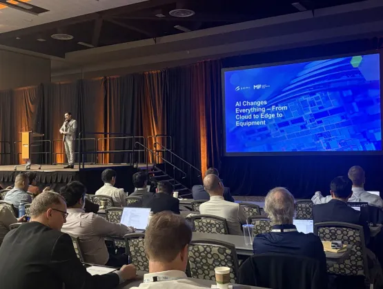
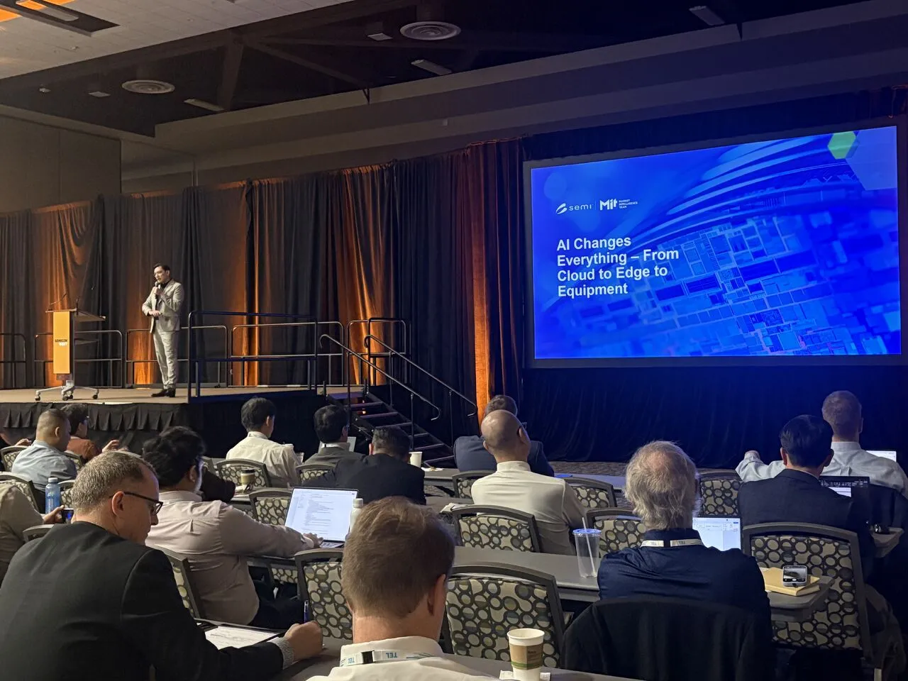
The 2025 SEMICON West Market Symposium brought together leading analysts and strategists to decode the powerful forces shaping the global semiconductor market. Building on last year’s focus on fabless growth and workforce initiatives, this year’s sessions centered on the rising influence of geopolitics, trade policy, and AI-driven investment. Experts from SEMI, Integrated Insights, Boston Consulting Group, Kearney, PwC, WSTS and TechSearch shared perspectives on how global shifts from tariffs to technology races are redefining supply chain resilience and regional competitiveness.On October 6 in Phoenix, Arizona, Clark Tseng, Senior Director of SEMI Market Intelligence, hosted the symposium and presented along with industry experts on the current trade environment from various angles. Discussions ranged from the effects of U.S. tariffs across the globe, to sector-specific considerations and market growth areas. US Trade Dynamics in Semiconductors As the geopolitical landscape in the U.S. becomes more complex, Iacob Koch-Weser, Associate Director, Global Trade Investment at Boston Consulting Group outlined the impact that tariffs are having on the U.S. industry. The average American tariff, he said, is higher than any time in the last 75 years. Although the semiconductor industry is less affected by high tariffs than other sectors, Koch-Weser noted that might change with the administration’s expanded Section 232 Tariff that imposes 50% tariffs on steel, aluminum, and their derivatives on nearly all trading partners. To explain, he described four potential Section 232 tariff scenarios, underscoring limited Section 232 enforcement as the ideal approach.Tariffs may be deprioritized in favor of chips incentivesThere may be targeted carveouts for alliesThe administration may impose high tariffs with limited exceptionsThere may be a 100% tariff rate To cope with tariff uncertainty, Koch-Weser recommended that companies consider reshaping policies, mastering trade compliance, and reconfiguring supply chains if possible. He also shared four potential outcomes for the future of U.S. trade that could take effect within the next 18-24 months. The U.S. may run its own system while the rest of the world aligns to World Trade Organization (WTO) rules.North American countries may form a stronghold, leaving all other countries to choose between the North American alliance and WTO standards.Countries may form new blocs and preferential agreements, creating multiple economic spheres worldwide.Global cooperation could break down, forcing countries to fend for themselves.With everything considered, he reinforced that the U.S. is still an attractive place for semiconductor investment. The current administration, he said, recognizes the importance of bringing advanced technologies back to the U.S. Navigating Uncertainty: AI-Driven Growth and the U.S. Semiconductor Manufacturing RenaissanceContinuing discussions on tariffs, SEMI’s Clark Tseng painted a picture of the current U.S. semiconductor industry. He divided his presentation into four key areas: near-term economic uncertainty, AI changes everything, semiconductor market equipment forecast, and material market outlook.Near-term economic uncertainty: U.S. tariff policies are contributing to inflationary pressures and altering global trade patterns, leading to cross-border uncertainty that is slowing investment. U.S. tariff revenue, he said, has expanded from $7 billion in January 2025 to $29.5 billion by August, forcing companies to sacrifice margins to compensate. AI changes everything: By 2030, Tseng noted that nearly half of the semiconductor industry’s capital expenditure will be driven by AI, pointing to sustained growth in AI-driven cloud infrastructure spending through 2028 forecasts. AI is also moving beyond data centers into edge computing and endpoint devices.Semiconductor market equipment forecast: Tseng reported that the outlook for the equipment market remains strong over the next three years. However, the biggest risk to the market is a potential slowdown in AI investment and adoption. Additionally, U.S. export controls and changes in regional supply chains present some challenges. Last year, China was the largest market for semiconductor equipment, but Tseng expects continued normalization amid broader market adjustments. Taiwan and South Korea experienced the strongest year-over-year growth, driven by demand for AI chips and high-bandwidth memory (HBM). Material market outlook: Silicon wafer shipments grew strongly in Q2 of 2025, but Tseng flagged this as unexpected and cited tariffs as a possible explanation. He noted the 300mm wafer segment is expected to grow 7% in 2025, while 200mm is projected to decline. The total wafer material market, he said, is also expected to grow by 6% this year. Additionally, wet chemicals experienced a 16% expansion in 2025, while silicon wafers, photolithography materials, and CMP materials are in recovery. Semiconductor Market – Status Outlook Tobias Pröttel (or Proettel), CEO of World Semiconductor Trade Statistics (WSTS), reported that the industry’s rebound remains firmly on track, with the latest WSTS statistics confirming a 19% year-over-year increase in global semiconductor sales during the first half of 2025. Total revenue reached $346 billion over the period, supported by strong demand for AI-driven infrastructure and next-generation data centers. Based on this solid first-half performance, WSTS has raised its full-year 2025 forecast to $728 billion, representing 15% annual growth, and now expects the market to reach around $800 billion in 2026, keeping the industry on course toward the $1 trillion milestone before the decade’s end.Logic and Memory continue to lead the expansion, driven by GPUs, AI accelerators, and high-bandwidth memory (HBM), while other product categories are showing steady recovery after the recent downturn. Pröttel noted that this growth is not confined to a single region: the Americas, China, and Asia Pacific are all posting double-digit gains, reflecting strong global momentum across the semiconductor value chain.Strategic Approaches to Semiconductors by Major Economies Following Pröttel, Kearney’s Vice President, PERLab, Sanjay Kumar outlined the semiconductor investment climates in South Korea, Japan, Taiwan, and India. South Korea is currently focused on maintaining its lead in memory, diversifying into logic, localizing its supply chain, developing advanced packaging capabilities, and investing in startups. Kumar also noted the Korean approach of offering loans, as opposed to the U.S. strategy of providing direct grants. In addition, Kumar said the Korean government plays an active role in how it wants its companies to grow, whereas the U.S. takes a more passive approach in this regard.Japan is also honing its leadership in key areas like materials and memory, and Kumar also pointed to the country’s efforts to build additional advanced packaging capacity. Japan, he said, aims to grow its industry though a mix of grants, loans, and tax credits. Among the country’s notable subsidies include a 50% subsidy for TSMC – its largest so far – as well as a $4 billion subsidy for Rapidus. Taiwan’s semiconductor industry is critical for protecting its national security. As a region with limited land, power, and water, Kumar noted that Taiwan is currently focused on developing its talent base. Its government is offering tax credits for R D and equipment and up to a 50% cost share for R D projects. India, he said, has one of the most ambitious incentive programs in the world. Through its India Semiconductor Mission (ISM), the country offers a 50% federal subsidy, in addition to a 20-30% state subsidy in its quest to cover the entire semiconductor ecosystem. Kumar also spotlighted some of India’s successes – like the joint venture between Renesas, CG Power and Industrial Solutions, and Stars Microelectronics – to build a new OSAT facility.Adapting to New Policy and Navigating the U.S. Semiconductor Landscape – Insights from Taiwan Taiwan is a critical trade partner of the U.S., ranking fourth in total trade volume as of July 2025. With Taiwan’s stronghold on the U.S. chip ecosystem, Paul Poliakov, Senior Manager, International Tax Services, CPA at PwC Taiwan detailed both the bottlenecks and developments regarding Taiwan companies’ investments in the U.S. Among the investment bottlenecks he highlighted were higher costs of building facilities in the U.S., multiple layers of compliance requirements that may be intimidating for new market entrants, and complex visa and tax regulations. In addition, Section 232 investigations on semiconductors are ongoing, with several potential policy changes that could take effect. The pending United States-Taiwan Expedited Double-Tax Relief Act could help ease burdens, he said, but it has yet to pass in the U.S. Senate as of October 2025. If it passes, it will integrate benefits for Taiwanese individuals and businesses into the U.S. tax code, which could substantially benefit Taiwanese investment in the U.S., including manufacturing, services, distribution, and a wide variety of other industries. Furthermore, Poliakov suggested that businesses maintain flexibility in their investment strategies, engage with U.S. state and local governments that can offer investment incentives, and work with professionals to ensure regulatory compliance. Geopolitical Shifts in Advanced Packaging AssemblyIn the final presentation of the 2025 Market Symposium, Jan Vardaman, Founder and President of TechSearch International provided an overview of the current advanced packaging market. Although advanced packaging represents the highest growth area in the industry, Vardaman highlighted that packaging complexity is also soaring. R D, testing, and equipment support infrastructure, she said, are becoming more critical for meeting future packaging needs. Even though assembly is mostly done in Asia, new U.S.-based advanced packaging facilities from Amkor, TSMC, and others represent signs of change. Still, Vardaman noted that the U.S. has almost no capability to produce advanced IC substrates using build-up film, which are needed to support high density applications. In addition, she highlighted that building more silicon fabs on U.S. soil won’t solve its national security or supply chain concerns.For the U.S. to create a sustainable packaging ecosystem, Vardaman concluded that support of assembly facilities is crucial. Ultimately, businesses must be willing to pay more for U.S.-based packaging in favor of potential supply chain resilience and national security benefits. SEMI would like to thank all speakers, sponsors, and attendees for the success of this year’s Market Symposium. Explore the latest SEMI Market Intelligence reports, covering historical reporting, actionable foresight into emerging trends and technology investments to make confident, forward-looking decisions across the semiconductor and microelectronics value chain.Clark Tseng is Senior Director, Market Intelligence Team at SEMI. Nishita Rao is Director, Product Marketing at SEMI.
Read More
The semiconductor industry is undergoing a rapid transformation. Artificial intelligence (AI) applications, such as agentic and physical AI, push compute demands to unprecedented heights, prompting the semiconductor industry to push the boundaries of 2nm technology and beyond. Yet, as we move to these advanced semiconductor technology nodes, it has become increasingly challenging for academic research to remain closely connected with the fast-evolving industrial developments, limiting academic researchers in driving innovation. Europe’s NanoIC pilot line, a pioneering European initiative, hosted by imec, is addressing this challenge by offering pathfinding process design kits (P-PDKs). To cover the potential of these P-PDKs and their impact on Europe’s semiconductor ecosystem, we sat together with Professor Mehdi Tahoori (professor at Karlsruhe Institute of Technology) and Anita Farokhnejad (DTCO Program Manager at imec).SEMI: What exactly is a P-PDK, and how does it differ from traditional PDKs?Farokhnejad: At its core, a process design kit (PDK) is a software environment that enables circuit designers to simulate, validate, and optimize chip designs using realistic models of chip technology. Consider it a blueprint or a simulation toolkit allowing chip designers to explore performance, power, and manufacturability of a new chip architecture in a virtual sandbox. What sets P-PDKs apart is that they anticipate future technologies. Unlike traditional PDKs, which are based on existing technologies, P-PDKs are built on predictive models of future nodes and architectures. This allows researchers to explore system-level trade-offs, assess architectural implications, and prepare design flows before a technology reaches maturity. SEMI: Why are they so crucial for academia?Tahoori: For decades, academic researchers could contribute to semiconductor innovation using abstraction layers that allowed them to design and test new architectures without direct access to the latest technologies. This approach worked well until the industry reached the 20-nanometer node. At that point, the complexity of semiconductor design increased, with the introduction of advanced device architectures like FinFETs, nanosheets, Forksheets, CFETs, and novel integration solutions such as 3D stacking and chiplet integration.Transistor scaling in the AI eraTraditional abstraction models could no longer keep up with these advances, and the gap between academic research and industrial practice began to widen. This growing gap started to limit academia’s ability to participate in semiconductor paradigm shifts, such as CMOS 2.0 and new computing architectures. P-PDKs, enabled by the NanoIC pilot line, aim to bridge this gap, restoring the connection between academic thinking and industrial progress.SEMI: How does this support semiconductor innovation in Europe?Tahoori: Universities are ideally positioned to drive out-of-the-box innovation and invent new paradigms for computing. This is where universities truly excel. But to do that, they need access to the latest technologies and tools. We see for example a strong focus on the AI revolution and how the microelectronics industry is enabling that transformation. To meet the demands of AI applications and the computing power they require, we need to design new computing architectures based on advanced technology nodes. This is precisely the academic area of expertise. To design these new AI computing architectures, however, we need the most advanced technologies available. The P-PDKs for advanced nodes provided by the NanoIC pilot line now make this kind of research possible at universities. Something that was not feasible before.Additionally, the P-PDKs also provide an important reference technology and platform to benchmark and validate these innovations within a next-generation design roadmap. This means researchers can test their novel architectures against realistic process and performance metrics.SEMI: Are they only available for academia?Farokhnejad: The NanoIC P-PDKs are meant to be accessible to foster innovation across Europe’s semiconductor ecosystem. These advanced PDKs are therefore also available to European research organizations, startups, and industry partners. Access is facilitated through Europractice, where eligible users can apply by signing a Design Kit License Agreement (DKLA). Once approved, they gain access to the PDKs.SEMI: What other technology nodes are NanoIC’s PDKs addressing?Farokhnejad: The first P-PDK was released in June (first version of the N2) and supports frontside and backside routing with TSVM, standard cell libraries, and multiple VT flavors for early-stage design exploration. Upcoming releases include new versions of the N2 P-PDK, as well as A14 and A7 PDKs, eDRAM and SOT memory PDKs, and advanced interconnect solutions such as redistribution layers (RDL), hybrid bonding, and interposers.Those interested in learning more about the NanoIC ecosystem and the research enabled by the P-PDKs can meet representatives and partners of the NanoIC pilot line during SEMICON Europa, November 18-21 at booth C2417 in Messe Munchen. More information about the initiative is also available on the NanoIC website.BiosMehdi Tahoori, Professor Chair of Dependable Nano-Computing - Karlsruhe Institute of Technology Mehdi B. Tahoori is Professor and Chair of Dependable Nano-Computing at the Karlsruhe Institute of Technology (KIT), Germany, and guest professor at imec, focusing on CMOS 2.0 and future chip technologies. He previously worked at Xilinx (USA), Fujitsu Labs (USA), and served as a junior professor at Boston Northeastern University (USA) and as a visiting professor at the University of Tokyo (Japan). He earned his B.S. from Sharif University (Iran) and M.S./Ph.D. from Stanford (USA). Prof. Tahoori is Deputy Editor-in-Chief of IEEE Design and Test Magazine, is a former Editor-in-Chief of Elsevier Microelectronic Reliability and has chaired major IEEE symposia. His honors include multiple best paper nominations and conference awards, the US National Science Foundation Early Faculty Development (CAREER) Award (2008), an ERC Advanced Grant (2022), and an IEEE fellowship.Anita Farokhnejad, DTCO Program Manager - imec Anita Farokhnejad earned her PhD from Universitat Rovira i Virgili (Spain), specializing in FEOL and device modelling. She joined imec in 2021 as an R D Engineer, focusing on BEOL optimization and future roadmap development. Collaborating closely with integration and physical design teams, she develops models for PnR data analysis and BEOL optimization. Her recent work on the enhanced Ring Oscillator (eRO) model aids in the early assessment of new materials and BEOL boosters. In August 2023, she advanced to team lead for PDK Enablement, translating advanced semiconductor nodes into Pathfinding-PDKs. Farokhnejad is also dedicated to education, conducting courses that make sophisticated technological concepts accessible to both industry veterans and aspiring engineers. Currently, she serves as Program Manager of DTCO at imec, where her contributions continue to drive innovation in the semiconductor industry.AcknowledgementThis work was enabled by the NanoIC pilot line. The acquisition and operation are jointly funded by the Chips Joint Undertaking, through the European Union’s Digital Europe (101183266) and Horizon Europe programs (101183277), as well as by the participating states Belgium (Flanders), France, Germany, Finland, Ireland and Romania. For more information, visit https://www.nanoic-project.eu.DisclaimerFunded by the European Union. Views and opinions expressed are however those of the author(s) only and do not necessarily reflect those of the European Union or Chips Joint Undertaking. Neither the European Union nor the granting authority can be held responsible for them. SEMI ContactJames Lam, Business Development ManagerEmail: [email protected]
Read More
AI is proliferating rapidly, fueled by ever-larger models and data sets that are expanding AI use cases and improving its accuracy. Future computing systems are now required to simultaneously deliver high performance, process large amounts of data, and use the least possible energy. The growing energy footprint of AI and the strain it places on the power grid is an increasing concern for companies and even entire countries. This could adversely impact future growth and could slow the semiconductor industry’s march towards $1 trillion in revenue, which is largely driven by AI applications.This is a formidable challenge that cannot be addressed in silos by individual companies or even industry segments. The SEMI Smart Data-AI Initiative is exploring how to overcome this challenge with collaborative and innovative system-level solutions that connect the dots across the entire AI system stack. In March 2025, we hosted a successful workshop, bringing together industry leaders across the value chain for a day of thoughtful discussions and knowledge sharing. Building on this foundation, we developed an exciting Smart Data-AI session to be held at SEMICON West in Phoenix, Arizona on October 7 from 10:30 a.m.-4:40 p.m. The “Future of Computing: Energy-Efficient Computing for AI and Beyond” forum will bring together executives and thought leaders across the entire ecosystem – including design, fabrication, interconnects, system integration, hyperscale architectures, advanced materials, and emerging technologies such as photonics and quantum. Attendees will have a unique opportunity to get strategic perspectives from these distinguished experts and learn about exciting future trends.Why Attend?Gain insights from global leaders and learn about innovative paths towards an energy-efficient computing future.Network and build cross-industry collaborations for the next wave of AI, photonics and quantum.Promote a more sustainable path for continued growth of AI to benefit humanity and the planet.Join the SEMI Smart Data-AI initiative to develop solutions and take concrete actions to reduce AI’s growing energy footprint.Support the industry in achieving its goal of reaching $1 trillion in revenue. Speaker Highlights Include:AMD • Ciena • Hewlett Packard Enterprise • IBM • Merck KGaA, Darmstadt, Germany •Microsoft • Quantum Economic Development Consortium • Rapidus • Rigetti •Siemens AG • Stanford UniversityDr. Pushkar P. Apte is the Strategic Technology Advisor and leads the Smart Data-AI Initiative at SEMI.
Read More
Digital Twins are no longer a futuristic concept in semiconductor manufacturing—they’re fast becoming the backbone of next-generation fabs. But here’s the challenge: without a robust, scalable data platform to unify, secure, and interpret the torrent of information flowing across design, manufacturing, packaging, and test, digital twins cannot deliver their transformative potential. At SEMICON West in Phoenix, Arizona on October 6, 2025 from 1–5 p.m., join us for a high-impact technical workshop that explores how advanced data platforms are fueling the next wave of innovation—enabling smarter, faster, and more precise decisions across the semiconductor lifecycle.What You’ll Learn – Gain insights on proven reference architectures for scalable data platforms, integration patterns that support digital twin ecosystems, real-world use cases from fabs and OSATs applying AI/ML at scale, best practices in managing governance and security across complex data pipelines.Modern Data Platform Architectures – Designed for speed, scale, and semiconductor precisionBreaking Down Silos – Leveraging shared ontologies and data fabrics for seamless interoperabilityAI-Enhanced Digital Twins – Real-world deployments across fabs and OSATsFederated Learning in Action – Secure, multi-party collaboration without compromising IPData Security Governance – Proven practices for high-stakes manufacturing environments Distinguished Speakers – Hear directly from leaders advancing digital twin and federated learning initiatives at the SmartUSA Institute and across the semiconductor ecosystem. Anshu Bahadur, Senior Program Manager, Technology Communities at SEMI, will open the workshop and introduce speakers who will share how they’re building these next-generation platforms and deploying them across fabs, OSATs, and the full manufacturing flow. Following individual presentations, the session will close with a panel discussion featuring these executives. Ross Kunz, Director of Technology, SmartUSA Institute (Keynote Speaker)Dr. Adam Schafer, CEO, Athinia TechnologiesDhara Vaishnaw, Head of Solution Architecture, AWSDr. Gautham Unni, Head of Solutions and Business Development, Semiconductor, AWSJonathan Holt, Senior Director, Product Management, PDF SolutionsDr. Surya Kalidindi, CEO, Multiscale TechnologiesWho Should Attend? This workshop is designed for: Data Platform Architects building the next-gen semiconductor backboneSmart Manufacturing Engineers integrating fab and test dataAI/ML Practitioners scaling models into production workflowsInnovators shaping digital twin systems for complex, high-precision manufacturing Why Attend? Because the future isn’t waiting. Digital Twins, powered by scalable data platforms, are redefining how the semiconductor industry innovates, collaborates, and competes. Don’t just keep up with the future—build it. Anshu Bahadur is Senior Program Manager, Technology Communities at SEMI
Read More
As artificial intelligence (AI) proliferates rapidly, AI models and datasets are also growing rapidly in size. This growth far outpaces performance improvement in hardware systems, and is increasing AI’s energy consumption unsustainably. To address these challenges and explore collaborative solutions, SEMI’s Smart Data-AI Initiative - as part of its Future of Computing focus - recently hosted a day-long workshop on Sustainable AI Systems that brought together domain experts from the entire AI ecosystem. Speakers included industry leaders Applied Materials, AMD, Arm, ASE, Google DeepMind, IBM, Intel, Lam Research, McKinsey, Micron, NVIDIA, Qualcomm, SK hynix; exciting start-ups Cerebras, LightMatter, Mentium Technologies and Mueon; and leading-edge academic institutions, Stanford University and University of California, Davis Irvine. The keynotes, panels and spirited audience discussions covered novel devices, materials, advanced packaging, chiplets, photonics and architectures algorithms for data centers, cloud edge. This article synthesizes high-level insights from the workshop.The AI ImperativeThe day started with a basic question – why is AI essential to continued progress and prosperity? The answer lies partly in shifting global demographics, with the population aging in most developed economies. At the turn of the century, there were ~6 people in the workforce supporting each retiree, but projections indicate there will be only 2 active workers per retiree by 2050. In parallel, productivity growth rates have fallen to half of what is required. AI can help bridge this gap, if we can ensure continued progress of AI in a responsible and sustainable manner.The Energy WallA formidable roadblock to continued progress of AI is its rising energy demands. For example, the energy used by some large language models (LLMs) to run just one training cycle could be used to power thousands of homes. The switch to transformer models has increased AI-driven computing demand by a factor of 50 million over 5 years, and by some projections, this demand will consume half the world's generation capacity by 2050. This is clearly not sustainable! All players in the ecosystem are deeply committed to reducing AI’s energy consumption, and the industry has already decreased the energy used per token of computing by a factor of 100K in the past 10 years. However, the rapid growth of AI outpaces this, highlighting the huge challenge ahead.The System StackThis workshop was developed with the hypothesis that innovation is required across all segments, and an important first step is to initiate a dialog. Our highly distinguished speakers covered the entire solution stack, and while it is impossible to capture the ocean of insights that they shared, the following provides a flavor.Materials DevicesMaterials and devices used to build semiconductor chips form the foundation of the stack for all computing systems. Silicon substrates with copper interconnects remain industry’s mainstay, but are being augmented by innovative ideas. As device dimensions continue to shrink, novel 2D materials such as MoSe2, WSe2, ZrSe2 and NbP are being researched. While Si mobility degrades with decreasing film thickness, 2D materials maintain high electron mobility in thin-film substrates. These can be stacked to build 3D systems with lower power consumption than traditional planar structures. In parallel, novel device technologies such as gate-all-around (GAA) can provide power savings up to 25%.These novel materials and devices are complex, and require almost magical wizardry to build. For example, they may require depositing a stack of multiple defect-free films that are only a single (or few) atomic layer(s) thick, or etching a steep well that is one hundred times as deep as it is wide. It is an incredible accomplishment of the semiconductor industry to build these devices and chips successfully, but it is getting harder and more expensive. Consequently, AI is now being used as a tool to help with this ever-growing fabrication complexity of semiconductor R D and manufacturing. This is a synergistic virtuous cycle, where AI algorithms enabled by chips are used in turn to help with chip fabrication.System IntegrationThe next layer of the stack is the integration of individual devices into a system. Advanced packaging techniques, such as silicon or glass interposers (2.5D) for interconnecting chips, can reduce the communication distance and power consumption. These are often deployed for high-performance computing systems running AI algorithms. Beyond this, the industry is actively exploring 3D systems that are even more compact, both as multi-die 3D packages and as monolithic 3D chips.The concept of chiplets – smaller chips with specialized functions that can be assembled flexibly to optimize system performance – holds much promise. Industry consortia are developing protocols such as Universal Chiplet Interconnect ExpressTM (UCIeTM) to enable seamless integration of chiplets both in the planar and vertical dimensions. These advanced techniques pack more functional elements into increasingly compact form factors, but this proximity makes power delivery challenging and often generates intense heat. Much work is needed to ensure optimal power delivery and adequate thermal dissipation.Looking beyond traditional electronics, photonics represents an exciting opportunity. Most long-distance data communication is on fiber-optic cables and thus already photonic – bringing this to shorter distances can save energy while increasing bandwidth and performance. This requires efficient photonic-electronic integration at the packaging or even chip level, which is a major challenge requiring cross-disciplinary collaboration.Architectures and AlgorithmsAI algorithms need enormous amounts of data processing compared to traditional computing workloads. This requirement stretches (or breaks) the limits of traditional Von Neumann architecture, which requires frequent data movement between memory and processor elements for each computation cycle. Much of current architecture innovation focuses on bringing processor and memory elements closer to each other. System integration is already driving “compute-near-memory” architectures like high bandwidth memory (HBM). Other forward-looking implementations combine them into a single chip, known as compute-in-memory (CIM). Memory elements being explored for this purpose include resistive RAM (RRAM), phase-change memory (PCM), ferroelectric RAM (FeRAM) and magnetic RAM (MRAM). However, there is no one “perfect” memory – each has pros and cons in terms of latency, capacity, bandwidth, power consumed per operation, manufacturability, etc. Other researchers are also exploring devices like memristors for analog computing, which can improve energy efficiency for certain workloads.Finally, hardware-software co-optimization is crucial. Algorithms mismatched with the underlying system are energy expensive; conversely, co-optimized systems are highly efficient. While conceptually obvious, this is difficult in practice because development cycles are quite different – software algorithms can transform in a few months, while new hardware often takes years to develop. While some strategies can be used for mitigation – such as designing in redundancy/flexibility or making the hardware application-specific – much work remains to solve this conundrum.Pre-competitive Collaboration to Find SolutionsAll speakers emphasized that pre-competitive collaboration across the entire stack is critical, as these challenges are formidable and cannot be solved by one entity or in isolated silos. SEMI is a global and neutral organization with over 3,000 member companies, and is well-positioned to provide a pre-competitive collaboration platform to connect the dots across silos. In fact, SEMI’s mantra is “Connect, Collaborate, Innovate” – reinforcing its commitment to advancing the entire industry. For this purpose, SEMI’s Smart Data-AI Initiative continues to drive robust discussions on this topic – next there will be a roundtable discussion during SEMICON Southeast Asia, May 20-22 in Singapore, followed by a focused technology session at SEMICON West 2025, October 7-9 in Phoenix, Arizona. The overall objective is to move from “talking-the-talk” to “walking-the-walk,” towards creating system-level solutions for energy-efficient AI computing. Specifically, we want to identify the pre-competitive actions that could synergize individual innovations and make the whole greater than the sum of parts. Some ideas include collaborative proof-of-concept projects, industry standards and independent benchmarking. Come join us on this journey and connect with us at [email protected]. Dr. Pushkar P. Apte is the Strategic Technology Advisor and leads the Smart Data-AI Initiative at SEMI.
Read More
The world is abuzz with the new opportunities being created by artificial intelligence (AI), enabled by availability of unprecedented amounts of data. AI runs on the semiconductor engine, and in turn, creates a rising demand for semiconductor chips. The semiconductor industry is predicted to reach $1 trillion in revenue by 2030 by McKinsey Co., in large part due to the market demand for AI and data. There are, however, formidable challenges to overcome for this virtuous cycle to continue. The SEMI Smart Data-AI Initiative, together with the SEMI Future of Computing Think Tank, is working to help the industry address these challenges. This article paints the big picture and lays the groundwork for an in-person workshop on March 19, 2025, in Silicon Valley, where pre-competitive and collaborative solutions will be explored.“To unlock the full potential of AI, innovation is required across the technology stack – from the models and software to datacenter architecture, chip design and how those chips are made. Advancements in foundational semiconductor technologies will have a dramatic impact on system-level energy and cost reduction in the AI datacenter.” – Gary Dickerson, President and CEO of Applied MaterialsThe Performance ChallengeInvestment in AI system infrastructure is rising at a dizzying pace, with hundreds of billions of dollars being committed by individual companies as well as public-private partnerships around the world. AI models built on larger data sets generally deliver better results, so model sizes are growing exponentially each year, with leading-edge models requiring billions and even trillions of parameters. This is especially true with the rapid growth of the Large Language Models (LLMs) used for Generative AI. Can the foundational semiconductor technology keep up? Even if semiconductor chips were following the famous Moore’s Law, performance would only double every 2 years. The real pace of performance improvement is even slower, as leading-edge technologies are reaching physical limits of materials – with the tiniest patterned dimensions on chips now approaching the fundamental atomic separation distance. While semiconductor designers and process technologists continue to innovate with new materials, devices, 3-dimensional stacking and so forth, there remains a formidable challenge for silicon chips and hardware systems to keep up with the growth rate of AI models and data sets. The Energy ChallengeProcessing ever-larger data sets and AI models also requires increasing energy. A recent report by the US Department of Energy indicates that data center energy consumption tripled over the past decade and may triple again in just 5 years! Other analyses show that a single data center powered by 20,000 GPUs can consume almost 40,000 KW, which is enough to power 31,000 homes in the US! Consequently, it is challenging for data centers to meet their power needs through public utilities, and several hyper scalers are investing in nuclear power. This acceleration in AI energy demand is further exacerbated because silicon technology evolution no longer follows power scaling with “Dennard’s Law,” which states that power density remains constant as technology scales to tinier dimensions. In fact, energy consumption of silicon devices has been increasing with technology scaling for the last decade. These combined factors give rise to the second formidable challenge – energy consumption is rising unsustainably for AI systems.Exploring SolutionsAddressing these challenges requires innovation from algorithms and architecture to foundational silicon technologies. The following are illustrative examples (not comprehensive) spanning the entire AI system stack.At the software and algorithm level, innovators are finding ways to reduce model size and to use hardware more efficiently. For example, IBM’s Granite models are smaller in size, with less than a billion parameters. Similarly, Google's Gemma platform offers small language models (SLMs). The recent market disruption from the publication of the DeepSeek reasoning model suggests that relatively smaller domain-specific reasoning models may offer significant efficiencies. At the architectural level, multiple paths are being explored. Special-purpose (or domain-specific) processing elements can deliver improved performance at equal or lower power for specific tasks. Examples include Cerebras’ wafer-scale designs with optimized AI accelerators and Mueon’s system-scale integration solutions. Another innovation path focuses on bringing computing closer to the memory elements, where the data resides. This addresses the major bottleneck between processors and memory in the traditional Von Neumann architecture, which has been the mainstay of the industry since inception. In-memory or near-memory computing, such as memory-focused architectures from Micron or processor-in-memory (PIM) solutions from SK hynix, offer higher performance with lower energy consumption for certain workloads. In parallel, leading CPU and GPU makers like AMD, Intel, and NVIDIA continue to innovate with power-efficient solutions. And “Edge Intelligence” innovations – for example, internet-of-things (IoT) solutions from Arm and Qualcomm – help reduce the processing and power load on data centers by executing more operations on edge devices.Critical enabling technologies also contribute significantly. Advanced packaging, for example ASE’s heterogeneous integration solutions, enable efficient, high-performance computing by integrating multiple diverse components optimally. Another emerging development is the advent of “chiplets,” which split the chip into smaller parts, and enable special-purpose accelerator building blocks to be assembled with more general processor, memory, and interconnect elements. A well-developed chiplet ecosystem could provide silicon designers with more degrees of freedom to design optimized systems. Looking beyond electronics, the integration of photonics can enable low-power, high-bandwidth connectivity – for example, LightMatter’s silicon photonics interconnects and Ciena’s data center interconnects.Materials and devices form the foundation of the technology stack. Example technology innovations include Stanford University-led N3XT, a 3D solution that integrates multiple novel devices and materials including resistive and spin-torque transfer RAMs, carbon nanotubes and 2D materials. Similarly, a University of California-led effort synthesizes low-dimensional nanostructures, sensors, detectors and photonics in an integrated solution. Finally, advanced and innovative processes and equipment are being developed – for example, by Applied Materials and Lam Research – to fabricate these novel materials and devices.All these individual innovations are amazing and necessary, but are they sufficient? What if we could collaborate across the entire system and co-optimize hardware and software innovations synergistically? Could the integrated whole be greater than the sum of parts? What efficiencies could we unleash? And what business opportunities would this unlock?The SEMI Future of Computing workshop on March 19, 2025, seeks to answer these questions by uniting AI innovation leaders from industry, academia and start-ups, including most of the companies and universities mentioned in this article. We will begin building pre-competitive collaboration that breaks through silos and explores system-level solutions – with the ultimate objective of radically improving the energy-efficiency of computing for AI.Pushkar Apte is the Strategic Technology Advisor and leads the Smart Data-AI Initiative at SEMI.Jim Sexton is a Fellow at IBM.Melissa Grupen-Shemansky is CTO and VP of Technology Communities at SEMI.
Read More
With increasing demand for personalized smart devices, the MEMS and sensor market is undergoing rapid transformation. MEMS sensors are the backbone of smart wearable devices, seamlessly integrating multiple functions to monitor and simplify our day-to-day activities. As applications in healthcare, environmental tracking, and AR/VR expand, the need for ultra-compact, energy-efficient, and intelligent sensors is more critical than ever.In an exclusive conversation with SEMI, Stefan Finkbeiner, CEO of Bosch Sensortec, shared his perspective on the dynamic landscape of MEMS sensor technology. From Bosch’s evolution to a solutions provider with a focus on sustainability and market-driven innovations, Finkbeiner offered a deep dive into how Bosch Sensortec is positioning itself at the forefront of the industry. “We have to think in terms of the end application and determine what the right hardware and software configuration should be in order to provide solutions with the greatest benefit and flexibility.”Further insights into the future of MEMS and sensor technology will be shared by Finkbeiner during his keynote at the SEMI MEMS Imaging Sensors Summit on November 14, 2024, in Munich, Germany. Registration is still open.SEMI: Welcome, Stefan, and thank you for sharing your insights on advanced sensor technologies. Let’s start with a personal question: What motivates and inspires you about working in sensor technology?Finkbeiner: Sensor technology is very diverse and has significant impacts on consumers. We take pride in prioritizing consumers’ needs and benefits. True to the Bosch motto, “Invented for life,” we are committed to making life better, easier and healthier. This is demonstrated in our sensing solutions, which provide valuable data for fitness tracking in smartwatches, enhance the audio experience in hearables, and enable real-time monitoring of air quality to help individuals make informed decisions for a healthier environment. I am fascinated by technology advancements that are enabling the scaling of sensors—and the processing power and intelligence packed into these increasingly compact devices. For instance, our latest acceleration sensors for hearables are the smallest in the world and are nearly invisible at just 1.2 x 0.8 x 0.55 mm³.We leverage innovative wafer level chip scale packaging (WLCSP) to achieve this reduced form factor. These compact, feature-rich, high-performance accelerometers are easier to integrate in the latest generation consumer products where size and functionality are critical requirements.SEMI: How has Bosch Sensortec’s approach evolved over the years and what is the company’s primary focus today? Finkbeiner: We began our success story a few years ago as a hardware supplier, with one of our first applications being the 'Portrait-Landscape' function in smartphones. Over time, we’ve evolved into one of the leading providers of MEMS sensors.Today, we no longer see ourselves purely as a sensor manufacturer, but as a technology solutions provider. Our focus has shifted to think in terms of the end application and determine what the right hardware and software configuration should be to provide solutions with the greatest benefit and flexibility.Achieving this requires significant software and artificial intelligence (AI) development. In essence, we are optimizing software through self-learning models. Hardware remains essential for optimizing power consumption, with most sensors integrating a controller alongside the ASIC to enable seamless software integration.This unique software and hardware configuration unlocks exciting possibilities and broadens our market reach. We see significant growth in head-mounted devices, and we are actively working on related acoustics solutions.SEMI: Looking ahead, what trends do you anticipate will have the most significant impact on the MEMS sensors market?Finkbeiner: We see several trends that will significantly impact the MEMS sensor market. First, there is growing demand for personal health monitoring in consumer and mobile electronics. Wearable devices, in particular, are becoming essential tools for individuals to track their health and fitness status. This trend requires MEMS sensors to become even more accurate, with solutions that include sophisticated software algorithms to ensure reliability, accuracy, and reproducibility. As a result, AI and machine learning (ML) technologies will play a crucial role in enhancing sensor performance.A second important trend is the continued miniaturization of MEMS sensors. To meet customer demands, sensors must integrate more functionality, including edge-processing capabilities. For example, what once may have been a simple accelerometer with a step-counting algorithm is now evolving into a 6-axis Inertial Measurement Unit (IMU) with an integrated microcontroller and advanced AI/ML software. A great example of this is in True Wireless Stereo (TWS) earphones, where the IMU not only tracks steps but also enables complex tasks like dead reckoning and supports 3D audio—all within the tight constraints of a small TWS earbud housing. Low power consumption, as always, is a critical factor for these mobile devices to meet CE (Conformité Européenne) standards.Finally, we believe that smart glasses, augmented reality (AR) and virtual reality (VR) devices are poised to become the “next big thing.” These devices require advanced image projection optics that offer excellent optical quality, low weight, and ease of use to ensure consumer adoption. We believe our MEMS-based LBS (Laser Beam Scanning) solution is ideal for these applications. Additionally, the successful adoption of smart glasses hinges on high-performance MEMS sensors that are compact, accurate, and power-efficient—critical requirements for all-day wearability and functionality.These trends underscore the need for MEMS technology to evolve, integrating greater functionality, precision, and efficiency to meet the demands of next-generation consumer devices.SEMI: What are some of the biggest challenges facing the MEMS sensors industry today, and how can companies overcome them?Finkbeiner: One key challenge is that the smartphone market—arguably the most attractive market for a variety of MEMS and MOEMS sensors—has become more or less saturated. To stay competitive, MEMS companies must innovate existing products while also developing new, differentiated sensors and actuators for next-generation mobile products.SEMI: How is Bosch Sensortec supporting sustainability initiatives?Finkbeiner: We are helping to mitigate climate change with our low carbon footprint solutions.Up to 20% of annual global carbon emissions are caused by forest fires. This is equivalent to carbon dioxide emitted by all the vehicles driven worldwide. Our sensors can detect forest fires before they develop into wildfires by measuring various gases such as carbon monoxide and hydrogen. In parallel, we are working with our production partners to reduce our carbon footprint over the coming years, while also replacing or minimizing the use of environmentally hazardous chemicals, such as PFAS.SEMI: What are you most excited about for the MEMS Imaging Sensors Summit, and how do you think it will impact the European semiconductor industry?Finkbeiner: The European semiconductor industry has deep expertise in MEMS and sensor technologies, positioning it to make a significant impact in markets such as consumer health, optical sensing, and AR displays. By continuing to focus on sustainable solutions, we can drive even greater impact for the broader industry and secure Europe’s leadership in these growth sectors.I look forward to collaborating with industry peers at the Summit to define next steps needed to advance Europe’s leadership. The MEMS Summit is an invaluable opportunity to collaborate and drive progress, and I warmly invite my colleagues to join us in shaping the future of the European semiconductor industry.Dr. Stefan Finkbeiner Dr. Stefan Finkbeiner has been CEO and General Manager at Bosch Sensortec GmbH since 2012. He was born in 1966 in Freudenstadt, Germany. Stefan Finkbeiner held various senior positions at Bosch including Director of Sensor Marketing, Director of Corporate Research in microsystems technology, and Vice President of Sensor Engineering. He looks back on almost 30 years in semiconductor industry working in different positions related to sensor research, development, manufacturing, and marketing. Due to his wide experience in semiconductor and sensor industry, Stefan Finkbeiner is a recognized guest in panel discussions and as keynote speaker. SEMI ContactSitong He / Communications Manager, SEMI EuropeEmail: [email protected]: +49 151 5546 2638
Read More
In today’s rapidly evolving semiconductor industry, ensuring both precision and efficiency in manufacturing has become an increasing challenge, particularly as advanced technologies like MEMS and AI chips push the boundaries of design and production. Inspection methods that were once sufficient are now falling short, making room for cutting-edge solutions powered by artificial intelligence (AI). The introduction of AI-driven 3D X-ray inspection technologies is transforming the landscape, offering manufacturers a sophisticated tool to ensure quality control, while driving sustainable production strategies.SEMI spoke with, Joscha Malin, Product Manager, and Daniel Stickler, R D Expert for X-ray Imaging at Comet AG, Industrial X-Ray System Division, to explore how AI-powered 3D X-ray inspection technologies are shaping manufacturing. They delve into how these technologies address critical challenges during inspections and defect analysis, using tools such as Dragonfly 3D World software for user-friendly, AI-driven insights that facilitate effective decision-making.Further insights into the application of AI-powered 3D X-ray inspection technologies and their role in advancing MEMS manufacturing will be presented by Stickler at the SEMI MEMS Imaging Sensors Summit on November 14, 2024, in Munich, Germany. Registration is now open.SEMI: Thank you both for agreeing to share your insights. To start, can you explain the importance of inspection strategies in the context of MEMS manufacturing?Malin: As MEMS devices become increasingly miniaturized and complex, effective inspection strategies are crucial. These strategies not only accelerate the wrap-up of production processes, but also significantly enhance product yield. With tighter tolerances and various materials involved, ensuring the integrity and functionality of each component is more critical than ever. A robust inspection strategy allows us to catch potential defects early, which can save time and costs associated with rework or scrap.Stickler: The evolution of MEMS technology, particularly in AI chips, demands a higher level of inspection sophistication. Traditional methods may fall short in providing the necessary detail and speed, which is why we’re focusing on advanced solutions like our AI-powered 3D X-ray inspection.SEMI: Could you elaborate on how the 3D X-ray technology differs from conventional inspection methods? Stickler: The 3D X-ray technology we utilize acts as a bridge between traditional optical methods and standard 2D X-ray inspection. It offers high-resolution, three-dimensional images without damaging the samples. 3D X-ray technology emphasizes three main benefits: clarity, efficiency, and actionable insights. This means we can obtain detailed images that help us analyze components more effectively, allowing for real-time decision-making.Malin: Moreover, the clarity and detail provided by the 3D X-ray images are critical when it comes to defect analysis in MEMS devices. They allow us to assess mechanical, electrical, and assembly errors in ways that conventional methods simply cannot. This leads to a more reliable production process.SEMI: What specific MEMS defects can be effectively analyzed using this technology?Stickler: There are several types of defects we can analyze. For instance, we can detect mechanical defects such as stiction or fractures, as well as electrical failures like short circuits. The 3D X-ray inspection allows us to visualize these defects in detail. Additionally, we can monitor assembly errors, which are particularly important in complex MEMS devices where misalignments can lead to significant issues.Malin: I’d like to add that early detection of these defects is paramount. The faster we identify issues, the quicker we can implement corrective actions, thereby improving overall yield and reducing production costs.SEMI: You mentioned yield improvement earlier. Can you explain how your technology contributes to that?Malin: Our approach supports process optimization by providing information on product characteristics and, for example, allows us to identify trends early on that may lead to yield issues later. We also aim to accelerate new product introduction in the early phase by rapid feedback, saving time and cost. This is crucial because many defects may not be apparent until later stages of production. With our technology, we can monitor samples in real-time, allowing us to react promptly to emerging challenges.Stickler: By integrating this feedback loop, we can significantly shorten the time to market for new products. This is particularly beneficial in industries where speed and efficiency are essential.SEMI: Can you tell us about Dragonfly 3D World software and its role in this process?Malin: Dragonfly 3D World is a user-friendly software that leverages AI and, specifically, deep learning for image processing. It enables users to efficiently perform bump metrology and defect identification, for example, without needing extensive expertise in the field. The software makes complex processes manageable, even for operators who may not be specialists in image processing.Stickler: Beside MEMS and advanced packaging in GPU production, this software is indeed an “AI-for-AI” application. By utilizing deep learning, users can train models that adapt to various imaging tasks, making the entire inspection process more efficient. The insights generated from the 3D X-ray images are automated, enhancing usability and streamlining workflows.SEMI: In conclusion, what are the key takeaways you’d like to share?Malin: The key takeaways are that AI-driven 3D X-ray inspection is transformative for the MEMS manufacturing process, enhancing inspection strategies and defect detection significantly. By integrating advanced technologies, we can ensure higher product quality and efficiency.Stickler: Yes, and I would emphasize the importance of powerful monitoring and non-destructive test tools. Our innovative solutions not only improve yield, but also pave the way for sustainable practices in manufacturing, ultimately benefiting the industry. Dr. Daniel SticklerDirector X-ray Technology Components at Comet AG, Industrial X-Ray System Division. Based in Hamburg, Germany, he holds a PhD in Physics from the University of Hamburg and has extensive experience in X-ray imaging, semiconductor X-ray applications and product innovations. Joscha MalinDirector Product Marketing Software Products at Comet AG, Industrial X-Ray System Division. Based in Hamburg, Germany, he holds a degree in Electrical Engineering with specialization in Semiconductors and profound experience in the industry. For over a decade, he has focused on developing X-ray inspection and metrology solutions, especially for the Semiconductor industry. SEMI ContactSitong He / Communications Manager, SEMI EuropeEmail: [email protected]: +49 151 5546 2638
Read More
SEMI Korea Members Day 2025 in September featured a wealth of insights on semiconductor industry market and technology trends. As the two-year semiconductor inventory correction eases, Soo-Kyoum Kim, vice president at International Data Corporation (IDC), provided a market update during his address to the event’s 400 attendees at the Suwon Convention Center. He highlighted that the semiconductor market is showing signs of gradual recovery, with growth predicted for the second half of 2024 and into 2025. This growth, he said, is being fueled by rising demand for artificial intelligence (AI) and high bandwidth memory (HBM). He projected that the total semiconductor market would grow to $779.8 billion in 2025, marking a 15.8% increase from this year's estimate of $673 billion. By next year, the memory market is expected to rise by 24%, largely driven by demand for AI. Although consumer demand will likely weaken due to a slowdown in the Chinese market, Kim shared that easing inventory adjustments will lead to a rebound during the second half of 2024, particularly in the growth of DRAM and NAND. Kim also predicted that the non-memory market, which reached $503.4 billion this year, will grow to $569.4 billion by 2025.Additionally, the compound annual growth rate (CAGR) for semiconductor network and data center sales is projected to be 26.4% and 16.2% by 2028, respectively. Kim explained that the strong demand for AI semiconductors in data centers and networks will help the semiconductor market maintain an 8% CAGR over the next five years, following the 2023 market adjustment.SEMI Korea Members Day HighlightsH.D. ChoThe AI-driven industrial transformation is demanding more advanced processes. To accommodate AI, the industry has shifted its focus away from miniaturization toward back-end processes. However, the challenges facing Korea's semiconductor industry have also intensified. Leading semiconductor research firms shared in-depth market forecasts and presented their latest semiconductor technology roadmaps, offering insights on business strategies for Korea’s semiconductor ecosystem.In his opening remarks, H.D. Cho, president of SEMI Korea, expressed deep gratitude for the exceptional resilience of SEMI Korea’s members, who continue to overcome roadblocks despite global uncertainties. He also highlighted the growth of SEMI Korea’s member companies, emphasizing their positive role in the global semiconductor supply chain, as well as SEMI's ongoing commitment in supporting their innovations.Call for Renewable Energy Policy Reform to Achieve Net ZeroBora Lee, leader of Solutions For Our Climate (SFOC), emphasized the strong correlation between the semiconductor industry and Korea's economic growth. Lee also outlined key factors contributing to the high costs that hinder renewable energy adoption in the semiconductor sector. "Korea's levelized cost of electricity (LCOE) for renewable energy is about 2-3 times higher than the global average," she said. "The establishment of a policy council involving semiconductor companies is a crucial step in developing cooperative strategies to promote the use of renewable energy." In addition, Lee stressed that collaboration among suppliers, consumers, and policymakers is necessary to address these barriers and accelerate the transition to renewable energy within the industry. AI is Reshaping the Global Memory MarketPeter Lee of CITI Group shared that the convergence of cloud and edge computing is helping support new demands from AI, the metaverse, and automotive applications. As a result, this will increase long-term demand for memory. "The growing demand for AI is diversifying the memory market," Lee said. "This includes products such as HBM, LLW, LPDDR5T, and CXL, all of which are expected to see increased adoption according to AI computing requirements."As the need for parallel processing in AI training and inference tasks grows, Lee predicted the demand for HBM3 and DDR5 will significantly rise. HBM's share of total DRAM revenue is expected to increase dramatically – from 11% in 2023, to 30% by 2027. Expected Growth of the GaN Power Semiconductor MarketHo-Young Cha, a professor at Hongik University and co-founder and CTO of ChipsK, highlighted that the GaN power semiconductor market is expected to see continuous growth due to its advantages over silicon-based devices. The expansion of GaN technology applications in various industries, including consumer electronics, automotive, and telecommunications, he said, will drive additional growth."The GaN power semiconductor market will grow from $180 million in 2022 to $2.04 billion by 2028," said Cha. Growth Outlook for the Semiconductor Equipment and Materials Market in 2025 Clark Tseng, director of the SEMI Market Intelligence Team, projected that the short-term outlook for the global semiconductor market will gradually recover due to improvements in end-demand for major electronic product sectors and surging demand for AI chips. "The equipment and materials markets are expected to show a slight improvement in 2024, with a strong recovery anticipated in 2025," Tseng stated. He noted that the equipment market would grow by approximately 3% in 2024 from $95 billion in 2023 and is expected to grow by 15% in 2025. Regarding wafer fab materials, the silicon wafer market is expected to decline from $14.1 billion in 2023 to $13.2 billion in 2024. However, recovery is anticipated to begin in the second half of 2024, with the market projected to reach a new record of $48 billion in 2025. For more insights on Korea and the industry, attend SEMICON Korea from February 19-21, 2025 at COEX Convention Exhibit Center. Visionaries and leaders will gather to discuss the latest developments, innovations, and business opportunities within the industry. As the region’s premier microelectronics event, SEMICON Korea 2025 is expected to host 70,000 attendees, 500 exhibitors, and 200 speakers. More event information, including registration details, will be available soon.Jaegwan Shim is Senior Specialist, Marketing at SEMI.
Read More