downloadGroupGroupnoun_press release_995423_000000 copyGroupnoun_Feed_96767_000000Group 19noun_pictures_1817522_000000Member company iconResource item iconStore item iconGroup 19Group 19noun_Photo_2085192_000000 Copynoun_presentation_2096081_000000Group 19Group Copy 7noun_webinar_692730_000000Path
Skip to main content
Default Banner Image

5G

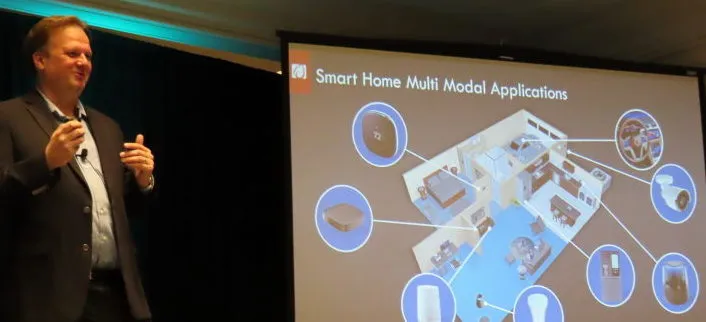
Key takeaway #2: If you need a Goldilocks process node – where you'll get just the right balance between active power, unit cost and investment – look to FD-SOI. And, btw, the IP landscape has improved dramatically. Those were just some of the great points made by Huibert Verhoeven (shown above), GM/SVP of Synaptics' IoT Division in his talk at the recent SOI Symposium in Silicon Valley.BTW, if you missed part 1 of our coverage --Silicon Valley SOI Symposium a Huge Success. Key Takeaways (Part 1) Here. – you’ll want to be sure to read it, too. Almost all of the presentations are now posted on our website – click here to access them.In this post here, we’ll cover presentations by Synaptics, GlobalFoundries, STMicroelectronics, Anokiwave and Dolphin Integration. It was a really full, day, so be sure to stay turned for Part 3 of our coverage to follow shortly: it will highlight the remaining presentations and panel discussions.Synaptics: Smart Home at the EdgeSynaptics’ Verhoeven’s presentation Revolutionizing User Experience Through Secure Neural Network Acceleration at the Edge was about Smart Home and using SOI. Synaptics is a human interface (HMI) company that’s been doing neural networks since 1986. They’ve always been on the leading edge, from their first shipment of PC touchpads to becoming a dominant force in all things HMI today: they now ship over a billion units annually. Synaptics slides 15 16 from the SOI Symposium, Silicon Valley 2019.They currently have SOI products shipping with dedicated neural networks for voice, he said. European [privacy] regulations have played a part in driving their use of SOI, as have challenges regarding power and heat. Things are getting smarter at the edge. For example, not only do users want their coffee machine to offer the usual morning espresso, Synaptics says that the next step is for your coffee machine to recognize you’re looking extra tired and ask if you might want a double?! For them Smart Home and multi-modal applications are the primary area of interest, as well as some automotive. Although their biggest customers have resources, others need guidance. Voice is a critical component, but now you also need video and display.Why SOI? Their HMI vision requires low power, significant computation and dedicated neural network hardware, explained Verhoeven, so FD-SOI with RF meets their needs. “22nm SOI is a Goldilocks IoT Process Node,” he proclaimed. It gets the combination of active power, unit cost and investment just right. What’s more, he said, “The IP landscape has improved dramatically. Our choice of SOI was not an accident.” Be on the lookout for more products leveraging FD-SOI over the next six months, he concluded. At this point on SOI, they’ve got 1 TOPS products with dedicated NPU for speakers, soundbars, Wi-Fi mesh, appliances, STBs and smart displays. These products have voice and sensor real-time (RT) AI. Next up is 4 TOPS on SOI with dedicated NPU, targeting STBs and smart displays with voice, video, imaging and RT AI. GF: World-Changing OppsGlobalFoundries slides 6 7 from the SOI Symposium 2019, Silicon Valley.“Our clients are at the forefront of changing the world,” declared Mark Granger, VP of the Automotive Product Line at GlobalFoundries. His presentation, Capturing High Growth Market Opportunities with SOI, detailed how mobility, automotive and IoT are the growth markets for SOI. So not unsurprisingly, GF’s 22nm FD-SOI technology, 22FDX, is seeing particular traction in mobile, edge, wearables and automotive. They’ve got twice as many tape-outs this year as they did a year ago, he noted. GF’s SOI portfolio includes 22FDX®, 45RFSOI and 8SW/7SW RF SOI for 5G/mobility; 22FDX for automotive (fully qualified for automotive Grade 2, with Grade 1 on the way); and 22FDX, 130RFSOI and 8SW/7SW RF SOI for IoT. GF has announced a stream of good news recently:with Dolphin Integration they’re delivering differentiated FD-SOI Adaptive Body Bias Solutions for 5G, IoT and automotive applications;they’ve crossed the billion-dollar design win threshold with 8SW RF SOI technology; they’ve collaborated with Synopsys to develop the industry’s first Automotive Grade 1 IP for their 22FDX process;and they worked with Rambus on the delivery of High-Speed SerDes on 22FDX® for communications and 5G applications.You might have heard about the Dolphin Integration news, as we covered it recently here at ASN (if not, be sure to read it here). Dolphin’s IP and methodology solutions address energy efficiency challenges. Automated transistor body biasing adjustment can achieve up to 7x energy efficiency with power supply as low as 0.4V on 22FDX designs. At the Silicon Valley event, Dolphin Integration CEO Philippe Berger provided additional information in his talk, FD-SOI IP Platform for Energy-Efficient IoT SoC. Dolphin Integration slides 5 6 from the SOI Symposium 2019, Silicon Valley.In another GF-related talk, Nitin Jain, the CTO of longtime GF RF-SOI customer Anokiwave presented Unleashing the mmWave Phase Array Using SOI for 5G Satcom. Anokiwave is a fabless semi IC company (you’ll find a good technical discussion of mmWave phase array written by their Chief Architect here). They do active antennas (aka phased array), something the military’s done for a long time, but now Anokiwave is bringing it to new markets and applications including radar, satcom and 5G. What they’ve been able to do is planarize the active antennas. They use GF’s 45RFSOI process technology for phased array systems because of the cost, performance, scalability and system enhancements it enables. 45RFSOI, he explained, is ideal for beam-forming FEMs (including the switches, LNAs and PAs). The move to 5G/mmWave is going to require a lot of antennas, so these Anokiwave ICs are headed to high volumes, concluded Jain.Stellar by STAs Roger Forchhammer, Director of Business Development at STMicroelectronics pointed out in his presentation, Automotive FD-SOI Microcontrollers with Embedded PCM, ST pioneered FD-SOI (and that was almost a decade ago, btw). Then in February 2019, they announced a world first: they’d begun sampling 28nm FD-SOI microcontrollers (MCUs) with embedded non-volatile memory (eNVM) based on embedded Phase-Change Memory (ePCM) to 10 alpha customers. These MCUs target powertrain systems, advanced and secure gateways, safety/ADAS applications, and vehicle electrification.STMicroelectronics slides 9 10 from the SOI Symposium 2019, Silicon Valley.(In case you want technical details, the breakthrough ePCM eNVM was first presented at IEDM in December 2018 – you can get the presentation that accompanied the paper, Truly Innovative 28nm FDSOI Technology for Automotive Microcontroller Applications embedding 16MB Phase Change Memory, from the ST website.)In his Silicon Valley presentation, Forchhammer said they’re now doing Stellar, a whole family of automotive products on FD-SOI. To do it, they’d taken an existing device and moved it to 28nm FD-SOI with ePCM, which they manufacture at their fab in Crolles, France. A major advantage for automotive he cites is that in software updates it’s bit-level programmable. “ST is fully behind FD-SOI,” he concluded, adding that we’re see more automotive as well as IoT products coming soon. Well folks, that’s all for this post. We’ll finish up our coverage of the SOI Consortium’s 2019 Silicon Valley Symposium in the next ASN post (there was so much to cover!). So please stay tuned.
Read More
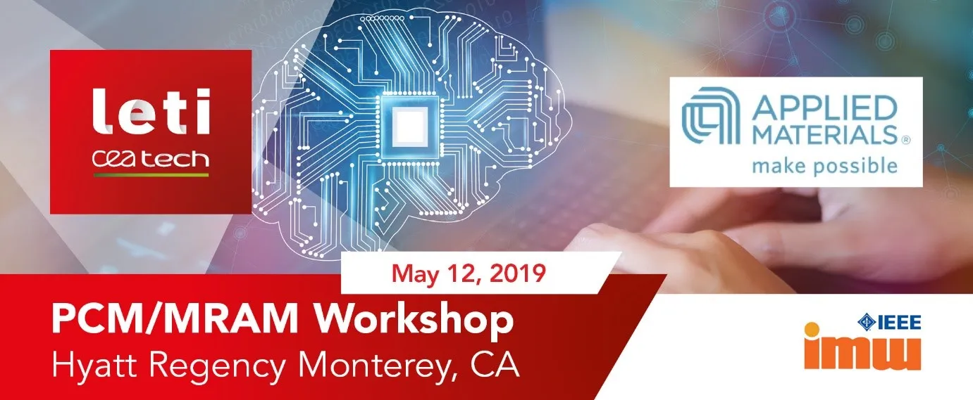
Two of the big, recent breakthroughs in memory technology – eMRAM and ePCM – have gotten their start in volume manufacturing on 28nm FD-SOI. In conjunction with the 2019 IEEE International Memory Workshop, SOI Consortium members Leti and Applied Materials have teamed up to give a technical program to explore short-term and long-term memory solutions. While the workshop is not specific to SOI, given the recent foundry announcements about ePCM and eMRAM for FD-SOI, the organizers predict it will be of particular interest to those following the greater SOI ecosystem. The event takes place at the end of the Sunday IMW tutorial day, starting at 5:30pm at the Hyatt Regency in Monterey, CA. Please see this page for the program and registration information. Here is the program: Emerging Non-Volatile Memory Promises Toward New Energy-Efficient Design and Applications - Michael Tchagaspanian, VP Business Development, CEA-Leti Technologies That Enable MRAM and PCRAM in Volume Manufacturing - Kevin Moraes, Vice President, Metal Deposition Products, Applied Materials Technology Improvements Directions of Emerging Non-Volatile Memory for New Applications Solutions - Etienne Nowak, Head of Memory Laboratory, CEA-Leti Integration Schemes and Challenges for New Memories in a New Artificial Intelligence Era -Michel Frei, Director, Advanced Product Technology Development, Applied Materials Jean-Eric Michallet, Head of Leti’s Microelectronics Components Department, Silicon Component Division is one of the organizers. Here is his overview: FD-SOI is expected to be a long-lived technology. It enables planar CMOS scaling and accommodates a great deal of More-than-Moore developments where its ability for low power and great analog performance can make a difference for IoT, Automotive, Machine Learning or 5G applications. But to do this it requires a high-performance and cost-effective non-volatile embedded memory option. The incumbent Flash cell is reaching the end of its roadmap due to the difficulty of shrinking the bitcell and manufacturing, as well as the finished wafer cost increase. Back-end integrated Random Access Memory in advanced CMOS process has been explored for many years now as a competitive solution for fast-write and low-voltage non-volatile embedded memories. Foundry availability of embedded Magnetic RAM and Phase Change RAM for FDSOI 28nm platforms has been announced recently, showing that these technologies have now reached industrial maturity. CEA-Leti and Applied Materials invite you to attend a technical program to explore short-term and long-term memory solutions, from early research to industrialization. Registration is open, free, and available to all IMW attendees, and others. However, as seating is limited and as we have already several participants pre-registered, registration is by invitation only and early registration is recommended. If you are interested, please email Jean-Eric Michallet. The event is presented in conjunction with the 2019 IEEE International Memory Workshop, to be held on Sunday, May 12th, 2019, Hyatt Regency, Monterey CA, starting at 5:30 pm.
Read More
Editor's note: Arm and Samsung Foundry are extending their collaboration on FD-SOI, which they'll be highlighting at the SOI Consortium's Silicon Valley Symposium April 9th. In the meantime, Arm Senior Product Marketing Manager Umang Doshi described the range of projects in a recent Arm Community / Developer physical IP blog. We thank Arm for sharing this blog with ASN readers.~ ~~ Samsung Foundry and Arm FDSOI collaboration announced By Umang Doshi The challenge with designing at newer and more advanced process nodes is that things generally don’t get less complex and expensive, much as we might want this. Still, the upside to each new process node, generally, is that you can build more highly efficient and targeted devices to address more markets and applications in a timely fashion. For the complexity and cost challenges, however, there’s good news: Arm and Samsung Foundry just announced a comprehensive, foundry-sponsored physical IP platform, including an eMRAM compiler at 18FDS (18nm FDSOI). In addition, the Arm offerings for 18FDS include three POP IP packages for Arm Cortex-A55, Cortex-R52 and Cortex-M33 processor IP. The platform will help drive new leading-edge designs in power-sensitive applications in 5G, artificial intelligence (AI), automotive, Internet of Things (IoT), and other market segments. It’s the industry’s first, fully comprehensive physical IP platform that includes an eMRAM compiler at 18FDS. 28nm: Before the breakthrough One of the most widely embraced nodes, 28nm the so-called “forever node,” has done wonders for industry innovation over the years. However, leakage power is still challenging for planar transistors. Engineers deployed high-K metal gate (HKMG) at 28nm, to combat leakage, but it’s still an issue. That’s because the channel underneath the gate is too deep and too far from the gate to be well-controlled, which results in higher leakage power. Solutions for the leakage issue have prompted designers to embrace FinFETs and FDSOI (fully-depleted silicon-on-insulator) with thinner channels that enable greater control by the gate. Indeed, FDSOI is gaining traction in the market place. By construction, 28nm FDSOI enables much better transistor electrostatic characteristics versus conventional bulk technology. 28nm FDSOI offers: Wide Forward/Reverse Body-bias range and flexible Poly bias (PB) range to tradeoff power/performance. Better performance and power than bulk process technology. Better resistance to radiation and SER. Less sensitive to variability because there’s no channel doping. Ultra-low power voltage (operating at low voltages in the hundreds of millivolts range). Easy migration from bulk versus the previous SOI version, PDSOI (partially-depleted silicon-on-insulator), required unique timing and power models. What’s more, there are cost benefits today and more forecast for the future. Arm and Samsung Foundry extend FDSOI leadership from 28FDS to 18FDS In 2018, Arm announced the industry’s first Embedded MRAM (eMRAM) compiler IP built on Samsung Foundry’s 28FDS process technology. Since the announcement, Arm has engaged with several Samsung Advanced Foundry Ecosystem (SAFETM) partners on a landscape-changing collaboration to deliver the industry’s first 28FDS eMRAM-enabled IoT silicon system demonstrator telling the Arm IoT story on Samsung Foundry silicon. Coupled with Arm’s IoT ecosystem, Pelion IoT Platform and Platform Security Architecture (PSA) solutions, this 28FDS eMRAM-enabled IoT demonstrator will showcase a new-generation of secure and energy-efficient IoT edge devices which integrates software stacks offering secure boot, firmware updates, on-chip storage, chip to cloud communication and device/software provisioning. The combination of 28FDS and eMRAM non-volatile memory brings new opportunities for a new class of highly integrated and energy-efficient designs. We’re thrilled that Samsung Foundry has extended its successful collaboration on FDSOI technology from 28FDS process to 18FDS. With the new platform, 18FDS is a cost reduction solution with lower power and same back end of line (BEOL) as 14nm FinFET. It has RF and eMRAM support to enable the widest range of different applications. “18FDS is the next-generation node on Samsung's FD-SOI roadmap with enhanced power, performance, and area (PPA)," said Jaehong Park, executive vice president of Design Platform Development at Samsung Electronics. “The relationship between Samsung Foundry and Arm stretches back more than a decade and has helped put the right design technology in the hands of the world’s leading designers. The enhanced PPA from our 18FDS process combined with Arm cores and Artisan Physical IP will again bring the cost and time-to-market advantages to enable the competitive and differentiated SoC designs.” Highlights on Arm-Samsung 18FDS platform Includes seven memory compilers, three logic libraries, two (1.8 and 3.3V) GPIO libraries, three POP IPs and the eMRAM memory compiler. Supports automotive AEC-Q100 Grade 1 design requirements, and comes with ASIL-D support and a complete automotive safety package. Utilizes back biasing supported by the FDSOI technology to help achieve low leakage by using reverse body-bias technique or a performance boost using forward body-biasing. This is a key differentiation of 18FDS platform. Supports Logic Corner Generator (LCG) and Memory Compiler Corner Generator (MCCG). LCG and MCCG products allow designers to generate custom corners with body-bias voltages to take the maximum advantage of body biasing power-performance flexibility. 18FDS will help enable the development of new devices connecting consumers in entirely new ways, whether it’s in AI, 5G mobile, automotive or other areas. The platform will be available in late 2019. Arm's Physical Design Group has a track record of successful implementations with Samsung Foundry across multiple generations of process nodes and products. Besides 28/18FDS, Samsung Foundry and Arm also have 14LPP/LPC, 11LPP, 7LPP and 5LPE platform collaborations. Interested in knowing more about Artisan Physical IP at 28/18FDS? Come join us at SOI Silicon Valley Symposium on April 9 at Double Tree by Hilton, San Jose, California. During the event, you will have the opportunity to hear how Arm and other industry leaders work together to accelerate the adoption of FDSOI technologies including products and applications. Alternatively, you can also reach out to us with your inquiry.
Read More
FD-SOI for RF and mmWave communications is a hot topic. In high-data rate communications like RF and millimeter-wave devices in particular, FD-SOI delivers high-performance with numerous unique advantages, making it most likely the fastest RF-CMOS technology on the market. If you’d like to take a deep dive and learn more about it, Soitec and Incize are sponsoring a free, full-day workshop in Grenoble on April 4th, 2019. Click here for registration information. The workshop follows the day after the IEEE/EDS EuroSOI-ULIS conference there (you can read about the full conference in a previous ASN post). This technical workshop will cover the FD-SOI technology platform with a focus on its compatibility with RF mmWave communications. Attendees will hear from notable FD-SOI leaders and experts from leading industry and research institutions presenting updates on key developments and building blocks across the semiconductor value chain. Topics will include circuit design, device fundamentals, simulation and characterization of RF devices, test, CMOS technology and substrate technologies enabling FD-SOI. In addition, the workshop will include an overview about how FD-SOI technology is benefiting current and future end user applications. Here’s the agenda: [caption id="attachment_15990" align="alignleft" width="945"] FD-SOI technology platform: new standards for emerging consumer electronics [Click to enlarge.][/caption]
Read More
GlobalFoundries and Dolphin Integration are collaborating on the development of a series of adaptive body bias (ABB) solutions to improve the energy efficiency and reliability of SoCs on GF’s 22nm FD-SOI (22FDX®) process technology for a wide range of high-growth applications such as 5G, IoT and automotive. The goal of the IP is to accelerate energy-efficient SoC designs and push the boundaries of single-chip integration. The design kits with turnkey ABB solutions will be available starting in Q2 2019. As part of the collaboration, Dolphin and GF are working together to develop a series of off-the-shelf ABB solutions for accelerating and easing body bias* implementation on SoC designs. ABB is a unique feature of FD-SOI that enables designers to leverage forward and reverse body bias techniques to dynamically compensate for process, supply voltage, temperature (PVT) variations and aging effects to achieve additional performance, power, area and cost improvements beyond those from scaling alone. The ABB solutions in development by GF and Dolphin consist of self-contained IPs embedding the body bias voltage regulation, PVT and aging monitors and control loop as well as complete design methodologies to fully leverage the benefits of corner tightening. GF says its 22FDX technology offers the industry’s lowest static and dynamic power consumption. With automated transistor body biasing adjustment, Dolphin Integration can achieve up to 7x energy efficiency with power supply as low as 0.4V on 22FDX designs. “We have been working with GF for more than two years on advanced and configurable power management IPs for low power and energy efficient applications,” said Philippe Berger, CEO of Dolphin Integration. “Through our ongoing collaboration with GF, we are focused on creating turnkey IP solutions that allow designers to realize the full benefit of FD-SOI for any SoC design in 22FDX.” “In order to simplify our client designs and shorten their time-to-market, GF and our ecosystem partners are helping to pave the way to future performance standards in 5G, IoT and automotive,” said Mark Ireland, vice president of ecosystem partnerships at GF. “With the support of silicon IP providers like Dolphin Integration, new power, performance and reliability design infrastructures will be available to customers to fully leverage the benefits of GF’s 22FDX technology.” As STMicroelectronics Fellow and Professor Andreia Cathelin has beautifully noted, “Body biasing is not an obligation. It’s an opportunity.” And GF/Dolphin clearly aim to make that opportunity a much easier and more powerful one to take advantage of. ~ ~ ~ *A note on terminology: the terms back bias and body bias are used interchangeably. Likewise the terms adaptive and dynamic when used in the FD-SOI context. Here is a quick explanation of how it works, from an ST paper from several years ago: Back-biasing consists of applying a voltage just under the BOX of target transistors. Doing so changes the electrostatic control of the transistors and shifts their threshold voltage VT, to either get more drive current (hence higher performance) at the expense of increased leakage current (forward back-bias, FBB) or cut leakage current at the expense of reduced performance. While back-bias in planar FD is somewhat similar to body-bias that can be implemented in bulk CMOS technology, it offers a number of key advantages in terms of level and efficiency of the bias that can be applied. Back-biasing can be utilized in a dynamic way, on a block-by-block basis. It can be used to boost performance during the limited periods of time when maximum peak performance is required from that block. It can also be used to cut leakage during the periods of time when limited performance is not an issue. In other words, back-bias offers a new and efficient knob on the speed/power trade-off. For another good discussion of body biasing in FD-SOI, you might want to check out The Return Of Body Biasing by Semiconductor Engineering's Ann Steffora Mutschler from a couple years ago.
Read More
Excellent news and exciting applications made headlines at the recent FD-SOI and RF-SOI events in Shanghai. During the FD-SOI day, Amazon/Blink and Intellifusion shared news about their new chips, and we got updates from GF and Samsung. The RF-SOI day featured a great talk with details about China Mobile's 5G plans, and peeks at Nokia's groundbreaking approach and Qorvo's outlook. [caption id="attachment_12354" align="alignright" width="300"] (Photo courtesy: Verisilicon)[/caption] The hall was absolutely full – with over 300 people attending each day. The FD-SOI event was by invitation only, and there were far more people wanting to attend than there was room for, even given the big room in which the events were held. The events got excellent coverage in the China tech press. For example, EEWorld started with an overview article and added five supporting pieces zooming in on key presentations and companies: one on GlobalFoundries, one on Samsung, one on Verisilicon, and two on Soitec (CEO and top exec interviews). These pieces are in Chinese, but just open the links through your favorite translation site. Many of the key slides are captured in these articles, so if you can't wait for the ppts to be posted on the SOI Consortium website, you can get some quick previews now. The Verisilicon PR folks also wrote up highlights of the FD-SOI event in real time with lots of great pictures – you can read that here. Many thanks to that team, too, for flagging the coverage in the China press and posting it on their WeChat account. On the RF-SOI side, the Simgui folks wrote that up – you can read it here. They also sponsored a gala dinner with awards given to Qorvo and SmarterMicro – you can read about that here. Most of the presentations will be posted on the SOI Consortium website over the next few weeks, at which point we'll cover them in-depth here at ASN. But for now, here's a quick round-up of some of the highlights. FD-SOI Highlights [caption id="attachment_12347" align="alignright" width="300"] (Courtesy: Blink, Verisilicon)[/caption] Boston-area based Blink, which makes very popular home security systems, was recently bought by Amazon (see their current product page here). They just taped out a new chip on Samsung's 28FDS FD-SOI technology, and they're really happy about it. “I believe for battery powered devices at home, FD-SOI is the way to go,” said Yantoa Jia, Head of ASIC China Ops at Blink. Their goal in the move from 55nm bulk to 28nm FD-SOI was to double battery life, add features and control costs: and they did it. Even adding two more CPU cores and lots more features, “The power drop is fantastic,” he said. Design was no problem, he continued, and there was plenty of IP. Once the new generation is officially announced, he promised to sit down with ASN and give us more details. Attendees also heard about a new chipset from Intellifusion, which is putting its face recognition technology onto GlobalFoundries' 22FDX FD-SOI with design house Verisilicon. CEO Nin Chen gave an impromptu talk about how their technology is used to find missing people and property. The new chip, which is especially designed for use in cities, is network-to-cloud leveraging AI. For his part Thomas Morgenstern, GlobalFoundries SVP and GM of the Dresden Fab 1, said they're seeing high yields and increasing capacity for 22FDX. The marketing and manufacturing ecosystem has been built around the fab in Europe. Now, he said, the key is to build an FD-SOI ecosystem in China. The market needs of China largely parallel those of Europe, he noted, for performance and efficiency at the right cost point. The ecosystem enables fast time-to-market and 1st-time-right. [caption id="attachment_12343" align="alignleft" width="300"] (Photo courtesy: Cadence)[/caption] Samsung SVP Gitae Jeong sees their FD-SOI technology as the right solution for the 4th Revolution, which includes everything from energy harvesting to self-driving cars. They've just taped out their first 5G mmWave cellular chip on 28FDS, he revealed. eMRAM is looking very good, only requiring three additional masks and getting stable yields from -40o to 105oC. 18FDS is on schedule, with PDK 0.5 now being released, and 1.0 on track for release in March 2019. They expect a very fast ramp, and are looking at a 35% area reduction, power cut in half and performance up 22% compared to 28FDS. RF-SOI Highlights [caption id="attachment_12350" align="alignright" width="300"] China Mobile, Project Manager Danni Song (Photo courtesy: Simgui)[/caption] When China Mobile talks, the world listens. Project Manager Danni Song presented again this year (she gave a great talk last year, too). China has a very ambitious 5G project underway, and under two years in which to roll it out. The biggest challenges are power consumption and cost (a problem made worse by the additional power amplifiers needed for MIMO). Can RF-SOI help solve these challenges, she asked? One thing she did clarify during the panel discussion was with respect to the mmWave part of the 5G puzzle. Their initial 2020 rollout will only focus on sub-6GHz, with mmWave following a year or two later. Michael Reiha, Head of RFIC R D at Nokia Mobile Networks clarified the worldwide 5G rollout during the panel discussion. Different locations on the planet have different histories and needs, so will rollout 5G in different ways. For historical reasons (and a lack of choice), the US will lead with mmWave, he said. Europe, meanwhile, will focus on 24GHz to meet the needs of automotive radar. In his presentation, Reiha described Nokia's approach to power amplifiers (PA), which is very different from what others are doing. With RF-SOI, he said, you can add sensors and logic for a level of preventative care, so you can gauge and protect your equipment using AI. He believes this disruptive approach will put them two years ahead of the industry, enabling massive MIMO to be deployed in dense urban areas with 60% lower power consumption and 50% savings in material costs. Go read about their Reefshark tech, he urged, which he says will beat GaAs. “The future is very bright with RF-SOI,” he concluded. “I can state that with confidence.” [caption id="attachment_12351" align="alignleft" width="300"] Julio Costa, Director of Technology Development, Qorvo (Photo courtesy: Simgui)[/caption] Julio Costa, Director of Technology Development at Qorvo sees it differently. Traditionally a GaAs house, all their RF-SOI work is fabless. While RF front end modules (FEMs) are loaded with RF-SOI, he said, and are a big winner for antenna tuning, Qorvo still sees GaAs for high-efficiency amplifiers and envelope tracking. But, he said, it will be a battle. GaAs wins in terms of area and power consumption he contends, but adds that SOI wins in terms of cost. Power levels, he predicts, will be the determining factor. So that's the quick overview – we'll drill down into the presentations as they're posted, so stay tuned!
Read More
Following the immense success of last year's FD-SOI training day in Silicon Valley, the SOI Consortium has another one planned for the end of April this year. If you want to start learning how to leverage FD-SOI in your chip designs, this is a great place to start. Click here for information on how to sign up. ST Fellow Dr. Andreia Cathelin has put together another great line-up. World renowned professors and experts from industry will deliver a series of four training sections of 1.5 hours each, focused on energy efficient and low-power, low-voltage design techniques for analog, RF, high-speed, mmW and mixed-signal design. You'll learn about design techniques that take full advantage of the unique features of FD-SOI, including body biasing capabilities that further enhance the excellent analog/RF performances of these devices. Each section of this training day will take you through concrete design examples that illustrate new implementation techniques enabled by FD-SOI technologies at the 28nm and 22nm nodes – and beyond. The design examples will cover basic building blocks through SoC implementations. A global Q A session will close the day. Here's a little more info on how the day will unfold. Click on the slides to see them in full screen. Morning sessionsFDSOI-specific design techniques for analog, RF and mmW applications - Andreia Cathelin, Fellow, STMicroelectronics [caption id="attachment_11714" align="alignleft" width="300"] Quick preview from Andreia Cathelin's FD-SOI training session (Courtesy: STMicroelectronics, SOI Consortium)[/caption] Andreia Cathelin is ST's key design scientist for all advanced CMOS technologies, and is arguably the world's leading expert on leveraging FD-SOI in high-performance, low-power RF/AMS SoCs. Her course will first present a very short overview of the major analog and RF technology features of 28nm FDSOI technology. Then the focus moves to the benefits of FD-SOI technology for analog/RF and millimeter-wave circuits. She'll give design examples such as analog low-pass filters, inverter-based analog amplifiers and 30GHz and 60GHz Power Amplifiers, as well as mmW oscillators. There will be particular focus on the advantages of body biasing and special design techniques offering state-of-the-art performance. Circuit Design Techniques in 22nm FD-SOI for 5G 28GHz Applications - Frank Zhang, Principal Member of Technical Staff, GlobalFoundries [caption id="attachment_11716" align="alignright" width="300"] Quick preview from Frank Zhang's FD-SOI training session (Courtesy: GlobalFoundries, SOI Consortium)[/caption] Frank Zhang has designed chips using GF's 22nm FD-SOI (22FDX) process for WLAN, 5G cellular and automotive radar applications. His course will focus on how to take advantages of FD-SOI’s high-frequency performance at relatively low-current density to design high performance RF/mmWave circuits. Examples circuits include a 28GHz LNA, a 28GHz PA and an RF switch for 5G applications. The FD-SOI advantages such as low capacitance, high breakdown voltage and high-output impedance will be exploited in these design examples. This course will also discuss how to extend these techniques to applications at higher frequencies and/or higher current densities that are subject to extreme temperatures and EM requirements. Afternoon sessionsEnergy-Efficient Design in FDSOI - Bora Nikolic, Professor, UC Berkeley [caption id="attachment_11715" align="alignleft" width="300"] Quick preview from Bora Nikolić's FD-SOI training session (Courtesy: UC Berkeley, SOI Consortium)[/caption] Borivoje (“Bora”) Nikolić is known as one of the world’s top experts in body-biasing for digital logic (he and his team have designed more than ten chips in ST’s 28nm FD-SOI.) If you missed it, his team's RISC-V chip was cited as one of Dr. Cathelin's “Outstanding 28nm FD-SOI Chips Taped Out Through CMP” – read more about that here. His talk at the training day will present options for energy-efficient mixed-signal and digital design in FD-SOI technologies. He'll explain how to generate body bias and use it to improve efficiency, with examples in RF and baseband building blocks, temperature sensors, data converters and voltage regulators. The techniques will be presented in the context of UC Berkeley's latest RISC-V-based SoC, designed to operate in a very wide voltage range using 28nm FD-SOI. mm-Wave and Fiber-Optics Design in FD-SOI CMOS Technologies - Sorin Voinigescu, Professor, University of Toronto [caption id="attachment_11713" align="alignright" width="300"] Quick preview from Sorin Voinigescu's FD-SOI training session (Courtesy: U. Toronto, SOI Consortium)[/caption] Sorin Voinigescu is a world renowned expert on millimeter-wave and 100+Gb/s ICs and atomic-scale semiconductor device technologies. His lecture will cover the main features of FD-SOI CMOS technology and how to efficiently use its unique features and suitable circuit topologies for mm-wave and broadband SoCs. He'll begin with an overview of the impact of the back-gate bias and temperature on the measured I-V, transconductance, fT, and fMAX characteristics. Then he'll compare the maximum available gain, MAG, of FDSOI MOSFETs with those of planar bulk CMOS and SiGe BiCMOS transistors through measurements up to 325 GHz. Next, he'll provide biasing, sizing and step-by-step design examples for VCO, doubler, switches, PA, large swing optical modulator drivers and quasi-CML circuit topologies and layouts that make efficient use of the back-gate bias to overcome the limitations associated with the low breakdown voltage of 20nm and 12nm FD-SOI CMOS technologies. Sign Up Now!With over 100 attendees filling every chair in the auditorium, last year's training day was sold out. Although it was in Silicon Valley, people actually flew in from all over the world to be there. During the Q A at the end, most everyone prefaced their questions by saying, “Thank you. I really learned a lot today.” 2018 will be no different – except that it's sure to sell out even faster. Please note, though, that this is not a free event, so only the attendees will get copies of the slide decks. Here's key info you need to sign up. See you there!What: SOI Consortium's FD-SOI Training DayWhen: 27 April 2018, 7:30am – 5pm.Where: Crowne Plaza San Jose, Milpitas CA (parking is free)Registration fee: US $485.00 (includes training book, breakfast, box lunch and refreshments during breaks)How to sign up: Click here to go directly to the registration site.
Read More
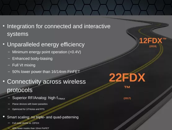
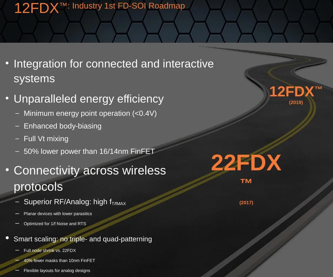
12nm FD-SOI has now officially joined the GlobalFoundries’ roadmap, targeting intelligent, connected systems and beating 14/16nm FinFET on performance, power consumption (by 50%!) and cost (see press release here). Customer product tape-outs are expected to begin in the first half of 2019. GloFo also announced FDXcelerator™, an ecosystem designed to give 22FDX™ SoC design a boost and reduce time-to-market for its customers (press release here). [caption id="attachment_9874" align="aligncenter" width="610"] (Courtesy: GlobalFoundries and SOI Consortium Shanghai FD-SOI Forum 2016)[/caption] The news turned heads worldwide (hundreds of publications immediately picked up the news) – and especially in China. "We are excited about the GlobalFoundries 12FDX offering and the value it can provide to customers in China," said Dr. Xi Wang, Director General, Academician of Chinese Academy of Sciences, Shanghai Institute of Microsystem and Information Technology. “Extending the FD-SOI roadmap will enable customers in markets such as mobile, IoT, and automotive to leverage the power efficiency and performance benefits of the FDX technologies to create competitive products." Wayne Dai, CEO of VeriSilicon (headquartered in Shanghai but designing for the world’s biggest names in the chip biz), added, “We look forward to extending our collaboration with GlobalFoundries on their 12FDX offering and providing high-quality, low-power and cost-effective solutions to our customers for the China market. The unique benefits of FD-SOI technologies enable us to differentiate in the automotive, IoT, mobility, and consumer market segments.” The ultra-thin FD-SOI wafers are where it all starts, and they’re ready to go in high volume, says Paul Boudre, CEO of SOI wafer leader Soitec. “We are very pleased to see a strong momentum and a very solid adoption from fabless customers in 22FDX offering,” he adds. “Now this new 12FDX offering will further expand FD-SOI market adoption. This is an amazing opportunity for our industry just in time to support a big wave of new mobile and connected applications.” All About 12GloFo’s 12FDXTM platform, which builds on the success of its 22FDXTM offering, is designed to enable the intelligent systems of tomorrow across a range of applications, from mobile computing and 5G connectivity to artificial intelligence and autonomous vehicles. Increased integration of intelligent components including wireless (RF) connectivity, non-volatile memory, and power management—all while driving ultra-low power consumption—are key 12FDX selling points that FinFETs can’t touch. The technology also provides the industry’s widest range of dynamic voltage scaling and unmatched design flexibility via software-controlled transistors—capable of delivering peak performance when and where it is needed, while balancing static and dynamic power for the ultimate in energy efficiency. [caption id="attachment_9873" align="aligncenter" width="610"] (Courtesy: GlobalFoundries and SOI Consortium Shanghai FD-SOI Forum 2016)[/caption] “Some applications require the unsurpassed performance of FinFET transistors, but the vast majority of connected devices need high levels of integration and more flexibility for performance and power consumption, at costs FinFET cannot achieve,” said GLOBALFOUNDRIES CEO Sanjay Jha. “Our 22FDX and 12FDX technologies fill a gap in the industry’s roadmap by providing an alternative path for the next generation of connected intelligent systems. And with our FDX platforms, the cost of design is significantly lower, reopening the door for advanced node migration and spurring increased innovation across the ecosystem.” Kudos came in from G. Dan Hutcheson, CEO of VLSI Research, IBS CEO Handel Jones, Linley Group Founder Linley Gwennap, Dasaradha Gude, CEO of IP/design specialists INVECAS, Leti CEO Marie Semeria and NXP VP Ron Martino (they’ve already started on 28nm FD-SOI for their i.MX line – read his superb explanations in ASN here). 22 Design Plug ‘n PlaySimultaneously to the 12FDX announcement, GloFo announced the FDXcelerator Partner Program. It creates an open framework under which selected Partners can integrate their products or services into a validated, plug and play catalog of design solutions. This level of integration allows customers to create high performance designs while minimizing development costs through access to a broad set of quality offerings, specific to 22FDX technology. The Partner ecosystem positions members and customers to take advantage of the broad adoption and accelerating growth of the FDX market.Initial partners of the FDXcelerator Partner Program are: Synopsys (EDA), Cadence (EDA), INVECAS (IP and Design Solutions), VeriSilicon (ASIC), CEA Leti (services), Dreamchip (reference solutions) and Encore Semi (services). These companies have already initiated work to deliver advanced 22FDX SoC solutions and services. Initial FDXcelerator Partners have committed a set of key offerings to the program, including: tools (EDA) that complement industry leading design flows by adding specific modules to easily leverage FDSOI body-bias differentiated features, a comprehensive library of design elements (IP), including foundation IP, interfaces and complex IP to enable foundry customers to start their designs from validated IP elements, platforms (ASIC), which allow a customer to build a complete ASIC offering on 22FDX, reference solutions (reference designs, system IP), whereby the Partner brings system level expertise in Emerging application areas, enabling customers to speed-up time to market, resources (design consultation, services), whereby Partners have trained dedicated resources to support 22FDX technology; and product packaging and test (OSAT) solutions. Additional FDXcelerator members will be announced in the following months.
Read More