downloadGroupGroupnoun_press release_995423_000000 copyGroupnoun_Feed_96767_000000Group 19noun_pictures_1817522_000000Member company iconResource item iconStore item iconGroup 19Group 19noun_Photo_2085192_000000 Copynoun_presentation_2096081_000000Group 19Group Copy 7noun_webinar_692730_000000Path
Skip to main content
Default Banner Image

Europe

The drive to scale nodes towards physical limits, known as "More than Moore," and the adoption of 3D architecture in chip integration strategies for advanced logic and memory applications has led to unprecedented demand for high-quality dependable materials solutions. With the aid of digital solutions, the process is expedited with higher quality and efficiency.SEMI spoke with Thorsten vom Stein, Director, Head of Process Design Semiconductor Materials at Merck KGaA, Darmstadt, Germany, about how materials innovations and advanced packaging can contribute to smarter supply chain solutions for a sustainable ecosystem.More insights into key aspects of 3D architecture in chip integration and heterogeneous integration will be shared at the Advanced Packaging Conference (APC) during SEMICON Europa 2024, Nov. 12-15 in Munich, Germany. Registration is open.SEMI: What makes the digitalization of chemical process design for semiconductor materials manufacturing so challenging at a technology level? Vom Stein: The primary challenge in digitalization of process design is achieving data rich experimentation and design flexibility from the start. When we begin the process design for a novel material solution, the freedom of design needs to be very high for optimal outcomes. For example, to identify the best sequence of unit operations to achieve best process intensification, do we need a distillation or extraction after the reaction to meet the purity requirements? At the same time, the samples from these early process trials need to have purity levels and process reliability standards for high-volume manufacturing of routine production in order to meet the requirements of our customers’ leading-edge chip integration strategies. We address this need by executing data rich experimentation starting with first trial, and thereby establish “production ready” data density in the lab.To avoid confining our design space, we therefore need highly “sensorized” and automated modular lab equipment that can give us the data density we need and flexibility at the same time.SEMI: Are data-driven approaches also applied to streamline manufacturing processes? Vom Stein: Yes, data-driven approaches are key to driving cost, quality, process reliability and sustainable excellence. As we scale up from lab experiments to high-volume manufacturing—often times increasing volumes by two or three orders of magnitude—we scale the process model virtually ahead of its physical twin to de-risk these major scale-up steps. An example of this is simulating the effect of reactor geometry on the impurity profile.Establishing this handshake between the physical asset and the process model early in the development has a lot of benefits for sustained cost efficiency of the future manufacturing process. For instance, it allows for optimization of yield and cycle times to the existing asset infrastructure. Furthermore, we can achieve quality reliability critical to our customers by establishing end-to-end correlation models that link the quality of incoming raw materials to finished good impurity profiles.Finally, we can achieve the lowest possible carbon footprint and minimize waste streams and energy intensity via process intensification by matching the unit operation sequence to the specific thermodynamics and kinetics of the process.SEMI: How can advanced packaging contribute to the pursuit of net zero? Vom Stein: Ultimately in a successful process design, we aim to achieve the maximum yield of value-added product with minimal input of resources and raw materials. So, there is an intrinsic synergy between highly intensified processes and their carbon footprint. The digitalization of process design allows us to track the CO 2 footprint during every iteration of the design. Establishing this tracking as a routine design KPI is one of the key initiatives to drive net zero semiconductor material solutions.In addition, advanced process design is a key enabler for circular value streams. We are currently working on multiple projects to recycle waste streams and re-feed them as raw materials in our processes. We are also exploring how our chemical process technology can aid our customers’ recycling efforts such as reusing lithography cleaning solvent waste streams.SEMI: In your previous talks, you emphasized the importance of diversity, equity and inclusion (DE I). How is this related to the digital revolution? Vom Stein: In the not-so-distant past, my team consisted mainly of process chemists and engineers. Now, we are working with data scientists, model developers, automation experts and many more substance matter experts on our projects. This work requires an inclusive culture to maximize the impact of these diverse sets of insights and disciplines.We also must acknowledge that, in many instances, we are exploring unchartered territory that requires a “leap of faith” culture trusting in digital models. Imagine, for example, a production plant director who is used to a stepwise physical scale-up, now being onboard with skipping physical scale-up steps by using predictive process models. It takes time to really establish a trust in the “power of data.” This type of culture is championed at Merck KGaA, Darmstadt, Germany on all levels: from CEO to the production operator. Our DE I Report showcases how we continuously build belonging for over 64,000 employees across the globe.SEMI: Merck KGaA, Darmstadt, Germany is a key contributor to semiconductor innovations. How important is it for Merck KGaA, Darmstadt, Germany to collaborate with other industry leaders to achieve goals in matters such as sustainability and DE I? Vom Stein: Collaboration with our customers and OEM partners is a key piece of achieving the molecular precision necessary to drive technology evolution that serves as the backbone to society. More and more, we need to link our material solution manufacturing process to the process parameters of the tools in the fab, ultimately improving the chip yield of our customers. To transition from the nanometer era to the angstrom era, we must establish these process correlations end to end along the value chain, which is why we are heavily engaged on our Athinia collaboration framework.Besides technology enablement, sustainability is the next avenue where cross value chain collaboration is a must to lower the CO 2 and energy footprint of our industry. To this end, we have started a joint program with Intel on AI-enabled sustainable semiconductor processes.The importance of industry collaboration is why I was so honored to participate at SEMICON Europa together with representatives from leading companies.SEMI: What did enjoy about SEMICON Europa 2023 that you would like to experience again in 2024? Vom Stein: I was really impressed by the SEMICON Europa 20 Under 30 recognition program launched during the show. The program honored the brightest young leaders who have demonstrated success in their careers in the microelectronics supply chain. We were very happy with the acknowledgement of one of our brightest minds at Merck KGaA, Darmstadt, Germany, Balazs Bordas, Digital Twin Implementation Lead. He has been instrumental for many of our pioneering efforts in this space.Such recognition programs are very important for our industry and can make a significant difference in the perception of the semiconductor industry and its ability to motivate and attract more talent. I personally hope to see similar programs in the years to come.Additional resources:Learn more about diversity and inclusion at Merck KGaA, Darmstadt, Germany.Learn more about Merck’s KGaA, Darmstadt, Germany modular lab automation approach.Merck KGaA, Darmstadt, Germany sponsored SEMICON Europa and SEMI Advanced Packaging Conference in 2023. Thorsten vom Stein is Director, Head of Process Design Semiconductor Materials at Merck KGaA, Darmstadt, Germany. Based in Darmstadt, Germany, he holds a PhD in Chemistry from the RWTH Aachen University and has extensive experience in Catalysis, Materials Science, Process Development and Value Chain Innovation.Serena Brischetto is Director of Marketing and Digital Engagement at SEMI Europe.
Read More
The Rising Stars: 20 Under 30 blog series celebrates the brightest young leaders shaping the future of the semiconductor industry. These exceptional individuals have earned the SEMI Europe 20 Under 30 Award for making a remarkable impact across the supply chain—whether in engineering, sales, marketing, or R D. The series spotlights these rising stars for their career achievements, commitment to innovation, leadership skills, and dedication to driving both business success and community growth.Follow their inspiring journeys, and discover how they are thriving and paving the way for future generations in the semiconductor world.Introducing Kai Hahn: Project Manager R D at Comet, Industrial X-Ray Systems DivisionKai Hahn’s journey began when he joined the company as a bachelor’s thesis student. His early drive and exceptional contributions quickly set him apart, earning him a role as a cooperative student while simultaneously serving as a "Change Manager." In this capacity, Hahn led high-impact business excellence initiatives, overseeing cross-functional projects at the executive level. Now, as a Project Manager in R D, Hahn leads agile teams developing cutting-edge automated inspection solutions. His leadership, marked by a commitment to innovation, collaboration, and customer satisfaction, drives both personal and organizational growth, making him a standout in the semiconductor industry.SEMI: What inspired you to join the semiconductor industry? Hahn: I didn't actively choose the semiconductor industry; rather, I grew into it together with our brands Comet Yxlon Dragonfly. Beyond the pioneering spirit our X-Ray System division has, what excites me the most is our direct connection to semiconductors. From turning off your morning alarm to driving to work, staying connected with friends and family, or watching a sports game on TV — semiconductors are everywhere and shape our daily lives. Working in this industry is both exciting and challenging. Every day, I look forward tackling new projects that push the boundaries of innovation. But what inspires me the most is the transformation that our division is undergoing. We are continuously adapting our processes and procedures to meet the growing demands of the market and our customers. Being part of this dynamic evolution is rewarding and exhilarating. SEMI: How did your early experiences and education shape your career path?Hahn: With my degree in business and engineering, I chose a program that covered a wide range of subjects. While I gained knowledge from a broad field, by the end of my bachelor's degree, I realized I lacked practical experience and a clear direction for my career.Joining Comet as an intern during my final year helped me anchor my career path. I decided to pursue my master's degree while working part-time for the company. This decision allowed me to gain relevant professional experience early on and apply the knowledge from my studies directly to real-world challenges. SEMI: Can you share a professional accomplishment you’re most proud of, and explain why it’s significant to you?Hahn: Combining the strengths of Comet Yxlon’s software and Dragonfly’s AI powerhouse — I was the dedicated project manager to support the global technological cooperation of our two software environments to accelerate the 3D IC go to market challenge. My goal was to facilitate methodological collaboration to develop new software inspection workflows for the semiconductor industry.Looking back, I am proud of what we accomplished: building a cohesive team from different cultures, working across time zones, adapting to various working styles, and successfully launching our first product.SEMI: As a young professional in the industry, what is your greatest challenge? Hahn: One of the biggest challenges is the rapid pace of industry change. For development teams, this means shorter development cycles and closer collaboration with international customers. For young professionals, it's essential to maintain a continuous learning cycle to stay current and develop the ability to work effectively across diverse cultures. This ensures we understand the different customer requirements and can implement them effectively.SEMI: What advice would you give to younger generations aspiring to make an impact in this industry?Hahn: Gaining practical experience alongside your studies as early as possible is crucial. Internships or working student positions offer valuable opportunities, and sometimes, it’s beneficial to proactively reach out to companies, even if no vacancies are advertised. For me, these experiences made my studies more engaging by linking theory to real-world applications and deepening my understanding of the subjects. Beyond acquiring practical skills and expanding your network, this approach helps clarify the career path you want to pursue after graduation.SEMI: How do you envision future work environments? Hahn: Working from home has increasingly become the standard in recent years. While offering many advantages, a significant challenge for companies is maintaining a sense of community. This is easier to achieve when employees are physically present, as in-person interactions tend to be more impactful. It raises the question of how companies can foster a strong sense of community and belonging in the long term without requiring workers to be physically present in the office.SEMI: What impact has the 20 Under 30 Award had on your career? Hahn: Overall, this recognition has been both a validation of my efforts and a source of inspiration to continue pushing the boundaries in my work. Beyond the recognition of my contributions and achievements, the award provided a platform to engage with like-minded young professionals beyond my usual network.Following 20 Under 30 JourneysKai Hahn’s journey from a bachelor’s student to a leading Project Manager at Comet, Industrial X-Ray Division is a testament to his dedication, innovation, and leadership in the semiconductor industry. His achievements in integrating teams, developing cutting-edge solutions, and driving organizational transformation highlight the significant impact young professionals can make. Hahn’s story is an inspiring example of how passion and perseverance can lead to remarkable accomplishments. As he continues to push boundaries and shape the future, SEMI looks forward to seeing the continued influence of his work in the semiconductor field.The Rising Stars: 20 Under 30 blog series celebrates the exceptional talent and leadership driving the future of the semiconductor industry. Each of the young innovators honored is not only excelling in their respective fields but also shaping the landscape of technology and business with their visionary approaches and dedication. Their stories exemplify the remarkable achievements and unwavering commitment that define the next generation of industry leaders. The series is intended to inspire and motivate future professionals to pursue their passions and embrace the opportunities within this dynamic industry. Stay tuned for more stories of rising stars who are paving the way for continued growth and innovation in the semiconductor world.Learn more about the SEMI Europe 20 Under 30 Award and the recipients honored at SEMICON Europa 2023. Nominations for the 20 Under 30 program at SEMICON Europa 2024 close on September 30.Maria Daniela Perez is Communications Manager at SEMI Europe.
Read More
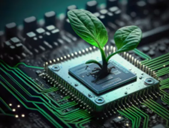
Silicon carbide (SiC), with its wide band gap and high thermal conductivity, is increasingly favored for semiconductor power applications across several fast-growing industries. Its ability to operate at higher voltages and frequencies enables significant efficiency gains, particularly in e-mobility, where SiC offers key advantages in size, weight, and speed compared to traditional silicon-based power devices.However, as promising as SiC is, the industry still faces critical challenges in scaling to meet growing demand. Key barriers include cost, reliability, and manufacturing capacity, all of which must be addressed for SiC to fully mature.SEMI spoke with Entegris Senior Director - Advanced Technology Engagements, Office of the CTO Mark Puttock, Ph.D., to discuss the challenges of scaling SiC power chip manufacturing from a material supplier’s perspective. Puttock shared insights ahead of his presentation at the Entegris session, Cultivating a Thriving SiC Market: Tackling Key Challenges Across the Value Chain, taking place on November 14, 2024, at SEMICON Europa in Munich, Germany. Don’t miss the opportunity to engage with experts from Entegris and other industry leaders. Registration is now open. SEMI: Global megatrends like environmental crises and AI drive the necessity for SiC power semiconductors. What is the current status? Puttock: The increasing demand for efficient power electronics — fueled by global megatrends such as vehicle electrification, environmental de-carbonization, and the rise of power-hungry AI chips — drives the necessity of wide bandgap semiconductors. SiC offers advantages of weight, size, and speed over traditional silicon (Si) solutions, which are particularly vital in automotive applications 600V and above. However, SiC chip manufacturing has not reached the maturity of silicon-based processing. Greater maturity will help reduce costs, which will accelerate adoption in the market.SEMI: What are the main challenges in scaling SiC?Puttock: Challenges in scaling SiC power chip manufacturing to high volumes are not surprising. That’s because high volume producers have not been operating long enough to resolve early-stage issues. From a material perspective, SiC is more challenging to manage compared to Si. The challenges we identify include:Chemical Mechanical Planarization (CMP): SiC is nearly as hard as diamond and significantly harder than Si, making it challenging to achieve a high removal rate while maintaining both planarity and low defectivity. This step is crucial toward the end of the wafering process and before the epitaxial growth of device layers.Handling: SiC is more brittle than Si, making it more susceptible to damage or breakage.Implantation: SiC is more difficult to implant than Si, requiring higher temperatures and the use of aluminum instead of boron as a P-type implant species. Additionally, it is a significant challenge to achieve a reliable aluminum source with a long and stable lifetime.Thermal Processing for Wafer Growth and Epitaxy Processes: SiC processes run hotter than Si ( 2000° C for wafering, 1500° C for epitaxial growth), demanding resilient chamber parts to achieve good lifetimes.Sustainability: Because SiC is extremely hard, the CMP process requires significant amounts of slurry. Improving slurry recycling and wastewater management continues to be a challenge.On October 29, we will address these issues in our webinar, “Challenges in Scaling SiC Power Chip Manufacturing: A Material Supplier's Perspective” This session will provide valuable insights and considerations for advancing maturity in high-volume SiC power chip manufacturing. SEMI: Can you elaborate on the challenges associated with CMP for SiC wafers? Puttock: SiC wafers are challenging to process, requiring specialized materials and methods compared to traditional silicon. Defects in the SiC wafer crystal during non-optimized CMP processing can propagate into the device epitaxial layers. This leads to yield loss, increased electrical resistance, reduced performance, and wasted power.SiC wafers must be cut, ground, lapped, and polished to create the necessary surface properties before depositing active layers. As the demand for these devices grows, optimizing the CMP process is essential to ensure the desired surface quality and planarity required for device fabrication. For a deeper understanding of these challenges, we recommend downloading our latest white paper, “Solving CMP Challenges in High-Volume SiC Production,” which covers:Achieving maximum smoothness with high removal ratesReducing the total cost of ownership Optimizing CMP slurry and pads for the unique wafer chemistry and topology of SiC wafersSEMI: What do you mean by optimizing slurry for SiC CMP?Puttock: CMP slurry typically consists of abrasive nanoparticle powder dispersed in a chemically reactive solution. The objective is to achieve a smooth, defect-free surface (less than 1 A Ra) with a high removal rate (greater than 7 µm/m).Traditionally, achieving high removal rates and smooth surfaces required two separate slurries. This approach sometimes forced SiC wafer manufacturers to choose a defect-free surface over a faster, more efficient CMP process, depending on their fab capabilities. Today, optimization allows SiC wafer manufacturers to achieve both high polishing capacity and good final surface quality using a single slurry.Additionally, while the slurry is the most critical part of the CMP process, the pad must be compatible with the application. This ensures the desired planarity while also preventing scratches or contamination of the SiC wafer surface. Research shows that optimized thermoplastic polyurethane CMP pads outperform traditional thermoset polyurethane pads. The optimized pads minimize surface damage and enhance removal rates due to their bulk hardness.SEMI: What are the future challenges for SiC devices? Puttock: SiC devices are increasingly favored for their superior energy efficiency and reduced environmental impact. However, the SiC manufacturing process presents challenges due to its high-temperature operations, which consumes significant amounts of energy and shortens the lifespan of chamber components. To address this, improving efficiency in these processes will be crucial in the coming years.Recycling is another important challenge. For example, CMP slurries present an opportunity for water recycling and conservation. At Entegris, we are committed to this issue and are actively collaborating with key industry players to enhance material circularity and prioritize sustainability in our new product development.SEMI: How is Entegris contributing to advancements in SiC technology, and what initiatives or partnerships do you have planned for the near future? Puttock: Entegris is an active member of the SEMI Global Automotive Advisory Council (GAAC) and participates in a working group focused on SiC with key industry leaders such as Volkswagen, BMW, Porsche Consulting, onsemi, Infineon, STMicroelectronics, and others. Our engagement spans the entire semiconductor supply chain, collaborating with integrated device manufacturers and original equipment manufacturers in fabs worldwide. Additionally, we recently announced our latest long-term agreement with onsemi, which underscores our commitment to advancing SiC technology.SEMI: What are your expectations regarding your participation at SEMICON Europa? Puttock: SEMICON Europa is a unique platform to connect with the semiconductor and automotive ecosystems. Last year, we organized a highly successful SiC session in collaboration with SEMI at both SEMICON West and SEMICON Europa, focusing on “Connecting the Automotive Ecosystem Towards More Mature SiC Manufacturing.”This year, we will continue the discussion with industry leaders during our session, “Cultivating a Thriving SiC Market: Tackling Key Challenges Across the Value Chain.” Our goal is to provide insights and propose solutions that will enable SiC power chips to achieve their anticipated role in future technology ecosystems.We will present alongside Porsche Consulting, and the talks will be followed by a panel discussion that will explore the current state and future prospects of SiC technology in power electronics. We invite visitors to join us at the Executive Forum on Thursday, November 14, from 1:40 – 3:00 p.m. and to visit us at Silicon Saxony booth 219 in Hall C1.About Mark PuttockMark Puttock, Ph.D., is the senior director of advanced technology engagements in the office of the CTO at Entegris. He has worked in the semiconductor industry for over 30 years with a background in physics and plasma processing. As a team member of the Entegris CTO office since 2014, Mark has followed technology trends and collaborated with Entegris’ global product development teams to develop timely and differentiated new materials, chemistries, and components for all the world’s semiconductor manufacturers. Maria Daniela Perez is Communications Manager at SEMI Europe.
Read More
Per- and polyfluoroalkyl substances (PFAS) are a large class of thousands of synthetic chemicals that are used throughout the semiconductor industry in the form of gases, liquids, and solid high-molecular weight polymers, due to their wide range of physical and chemical properties. PFAS contain carbon-fluorine bonds, which are one of the strongest chemical bonds in organic chemistry, allowing them to resist degradation and to cover long distances away from the source of their release.In recent years, the high persistence of PFAS in both the environment and the human body has encouraged the European Chemicals Agency (ECHA) to launch a PFAS restriction proposal aiming to regulate and eliminate their use over the next few years. The proposal is currently under assessment by ECHA’s scientific committees for Risk Assessment (RAC) and for Socio-Economic Analysis (SEAC).PFAS in the Semiconductor Industry The exceptional physiochemical properties of PFAS provide them a high degree of functionality in semiconductor manufacturing across the entire supply chain, and often the combination of their properties allows manufacturers to satisfy multiple and overlapping technical requirements.While the industry recognizes the importance of transitioning away from PFAS, and research to that effect is ongoing, current technological limitations do not allow the industry to manufacture semiconductors without the use of PFAS or to discover scientifically viable alternatives that can effectively substitute their use.At this point in time, no known alternatives exist for most of the uses of PFAS by the semiconductor industry. Alternative substances must be researched, invented and potentially applied into mass production to be recognized as viable alternatives. Many different pathways will have to be explored as PFAS are currently used across the entire supply chain for over 1,000 semiconductor applications, including articles, support equipment and fab operations, or as process chemicals.SEMI Europe—European Semiconductor Industry Association (ESIA) PFAS Research Workshop Considering the criticality of the PFAS issue for the semiconductor industry, SEMI and the European Semiconductor Industry Association (ESIA) have greatly strengthened their joint advocacy efforts over this past year concerning the ECHA’s PFAS restriction proposal.In this regard, SEMI and ESIA successfully organized a workshop in October 2023 with the relevant representatives of the European Commission (DG GROW, DG ENV, DG CNECT and DG RTD) to present and discuss in-depth the key technical evidence for the use of PFAS is the semiconductor sector. The discussions built upon the extensive technical evidence that was presented by SEMI and ESIA in their respective submissions for the six-month PFAS consultation facilitated by ECHA.Following the successful execution of this first workshop, there was a keen interest from the European Commission to enquire further upon the current state of play of research and development efforts in the field of PFAS detection, abatement, capture and destruction, circularity, recycling and alternativesFor this reason, after the first workshop, ESIA and SEMI collaborated to develop and deploy a joint PFAS Survey aimed at identifying the research priorities in PFAS from the perspective of their member companies. Based on the survey outcomes, the associations compiled the SEMI–ESIA PFAS Research Roadmap and officially presented it to the representatives of the European Commission during a follow-up workshop on 13th June 2024. Discussions at the workshop focused on the key research priorities for the semiconductor industry to discover potentially viable alternatives to the use of PFAS. In the upcoming legislative period, SEMI Europe will continue to engage with relevant stakeholders to contribute to the political debate and encourage a legislative framework that can enhance sustainability across industrial supply chains while preserving Europe’s technological competitive advantage. Get InvolvedGet involved in the SEMI PFAS Working Group! The SEMI PFAS Working Group is composed of industry technologists from leading companies across the global semiconductor manufacturing supply chain. The working group meets regularly to share intelligence and develop strategies to earn exemptions and/or extensions from regulators. Join SEMI in this crucial effort to enable the industry to continue manufacturing chips vital to the prosperity of the world by contacting [email protected]. Stefano Orlando is Manager Advocacy and Public Policy at SEMI Europe.
Read More