downloadGroupGroupnoun_press release_995423_000000 copyGroupnoun_Feed_96767_000000Group 19noun_pictures_1817522_000000Member company iconResource item iconStore item iconGroup 19Group 19noun_Photo_2085192_000000 Copynoun_presentation_2096081_000000Group 19Group Copy 7noun_webinar_692730_000000Path
Skip to main content
Default Banner Image

Workforce development

Nijmegen / Taipei, 26 August 2026 — Trymax Semiconductor Equipment (“Trymax”), a specialist manufacturer of plasma- and UV-based solutions for the semiconductor and optoelectronics industries, today announced that it has been awarded a substantial, multi-year, multi-million-dollar purchase order by Applied Optoelectronics, Inc. (AOI, Nasdaq: AAOI), a leading provider of advanced optical and HFC networking products that power AI. The award reinforces Trymax’s growing footprint in advanced semiconductor device manufacturing.

AOI grows and fabricates its own chips and wafers in-house, using Indium Phosphide (InP) to build lasers that are used in its optical transceivers for intra and inter-data center connectivity. InP-based laser manufacturing can present specific process challenges, particularly in handling fragile substrates across mixed wafer sizes—an area in which Trymax has established itself as one of the leading equipment suppliers for this class of device, based on its tool availability, innovative technology and wafer-handling capabilities.

Under the contract, Trymax will provide AOI with its Ashers and UV curing systems to support the chip-making process by removing residues, etching surfaces, and treating materials at various stages of fabrication. These platforms are capable of processing InP wafers ranging from three to six inches and are widely recognized for handling fragile substrates without compromising yield.

Commenting on the announcement, Garrie Murphy, Sales Director Americas at Trymax, said, “This award reflects the depth of engineering collaboration we've built with AOI over time. Our teams have worked closely to align our Ashers and UV curing platforms with the exacting tolerances their manufacturing processes demand, and this marks a natural extension of that partnership as their production needs continue to grow.”

Stephen Hu, Deputy Director of Wafer and Chip Production at AOI, highlighted the benefits of the partnership, adding, "Trymax is a trusted partner for plasma cleaning and UV/ozone surface preparation equipment, which we plan to integrate into our wafer fab in Sugar Land. In our evaluation, their equipment performed very well and their team has been highly responsive, which is critical for our partners as we aim to rapidly expand our laser chip production capacity in Texas.”

Trymax will be exhibiting at SEMICON Taiwan 2026, taking place September 2–4 at TaiNEX, Taipei. Visitors can learn more about Trymax's Ashers and UV curing solutions in the Netherlands Pavilion in Hall 1, K2760.

For more information, visit www.trymax-semiconductor.com.

ROSENHEIM, Germany, 10 July 2026 — esmo group (esmo), a leading global full-service systems integrator, developer, and supplier of advanced automation solutions, is marking its 25th anniversary in 2026 from a position of continued growth, having completed three facility expansions across Germany, China and Taiwan within a six-month period. The investments strengthen the company’s engineering, manufacturing and customer support capabilities in key semiconductor markets worldwide.

Engineering Growth Through 25 Years of Customer Trust

Today, the esmo Group employs approximately 285 people and generates annual revenue of around EUR 60 million through its two business divisions: semiconductor test solutions and special-purpose machinery.

Founded in 2001, esmo has grown from a small engineering company delivering just three manipulators in its first year to a globally recognised specialist serving customers in more than 70 countries. The company today produces more than 2,000 manipulators annually and is the world’s leading supplier in the segment. Its customer base includes leading semiconductor manufacturers such as CCTec, ADVANTEST, Infineon, Bosch, STMicroelectronics and Intel, with many customer relationships spanning more than 15 years. Notably, esmo’s very first customer remains an active customer today.

“Reaching 25 years is a significant milestone, but what matters more to us is what it represents — a track record built on engineering discipline and long-term customer relationships,” expressed Mr Andreas Rothstein, CEO of esmo AG. “The expansions we are completing this year are a natural extension of that foundation, and a clear signal of where we are headed.”

Expanding Presence Across Strategic Semiconductor Markets

As part of its latest growth phase, esmo has expanded its global footprint through three facility investments.

In Rosenheim, Germany, the company has established a new building adjacent to its existing assembly hall. The facility houses administrative functions as well as engineering and software development teams from esmo semicon. Following the building’s soft opening in November 2025, the site also hosted esmo’s 25th anniversary open house in June 2026, welcoming nearly 1,000 visitors for a behind-the-scenes look at its production and engineering capabilities, including technologies supporting advanced semiconductor test applications such as AI and high-performance computing (HPC).

In Shanghai, China, esmo has opened a new production facility featuring dedicated manufacturing space and a cleanroom environment. Focused on automated test equipment (ATE) and prober solutions, the site enhances the company’s ability to deliver precision assembly, quality assurance and local support for customers in one of the world’s largest semiconductor markets.

Meanwhile, in Zhubei, Taiwan, esmo has joined a new shared office established through an initiative led by Accuron Industrial Technologies, esmo's parent group. The facility brings together several Accuron portfolio companies, including RECIF Technologies, mechatronic systemtechnik, Trymax Semiconductor Equipment and NexGen Wafer Systems, strengthening collaboration and creating new opportunities to support customers across the semiconductor value chain in a strategically important market.

Investing in the Future of Semiconductor Test

Looking ahead, esmo is focused on advancing semiconductor handling technologies to meet the increasingly demanding requirements of AI, high-performance computing and other next-generation applications. At the same time, the company continues to expand its global service capabilities, invest in automation and digitalisation, and develop more sustainable manufacturing processes while building the next generation of engineering talent.

“The semiconductor industry is evolving faster than ever, and our customers need partners who can keep pace,” said Rothstein. “We’ve built our success on engineering excellence, reliability, and the ability to solve complex challenges. As we look to the future, we will continue to invest in our people, our technology, and our global presence to ensure that esmo remains the partner of choice for the world’s leading chipmakers.”

MILPITAS, Calif., May 26, 2026 — The SEMI Foundation, serving as the Hub Operator for the National Network for Microelectronics Education (NNME), today announced the launch of the first four Regional Nodes of the NNME, marking a major national milestone in the effort to build America’s microelectronics and semiconductor workforce at unprecedented scale.

Funded by the U.S. National Science Foundation Directorate for Technology, Innovation and Partnerships (NSF TIP) in partnership with the U.S. Department of Commerce and aligned with the CHIPS and Science Act, the NNME is designed to serve as national infrastructure for microelectronics talent development across the United States.  

The activation of the first Regional Nodes marks the launch of a connected national ecosystem designed to align industry demand with education, training, and career pathways that prepare new learners for high-demand careers powering the future economy.

The four Regional Nodes are:

  1. NNME Southwest, led by the Arizona Commerce Authority, serving Arizona, Southern California, Colorado, New Mexico, and Utah;
  2. NNME Pacific Intermountain, led by Boise State University, serving Idaho, Washington, Oregon, Montana, Utah, Colorado, Nevada, Northern California, and Hawaii;
  3. NNME Northeast, led by NY Creates, serving Connecticut, Delaware, Maine, Maryland, Massachusetts, New Hampshire, New Jersey, New York, Pennsylvania, Rhode Island, Vermont, and Virginia; and
  4. NNME South,  led by the University of Texas at Austin, and serving Arkansas, Mississippi, Georgia, Florida, Texas, New Mexico, Louisiana, Oklahoma, Utah, and Alabama.

Collectively, the four NNME Regional Nodes activate a national network of more than 325 performer organizations, including K-12 school districts, colleges and universities, workforce development organizations, economic development agencies, community-based organizations, and semiconductor employers working together to build stronger pathways into microelectronics careers for all Americans.

“America’s ability to lead in semiconductors depends on whether we can build and sustain the workforce needed to power innovation here at home,” said Senator Todd Young. “The National Network for Microelectronics Education represents the kind of national, industry-connected workforce strategy needed to strengthen America’s competitiveness, expand opportunity, and prepare the next generation of talent for high-demand careers in microelectronics and advanced manufacturing."

Under the NNME structure, the SEMI Foundation and NSF expect to support the four Regional Nodes with potential funding opportunities of up to $20 million per node over five years to accelerate scalable talent solutions aligned to industry demand and establish the gold standard for microelectronics education and workforce training across America.

Building the Workforce Required for America’s Semiconductor Expansion

"The launch of these Regional Nodes constitutes the activation of national infrastructure built to meet the most consequential economic and technological challenge of our time," said Shari Liss, Vice President of Workforce Development and Initiatives at SEMI and the SEMI Foundation.

“NNME is bringing together industry, educators, workforce organizations, and regional leaders to build a talent engine capable of preparing the next generation of semiconductor workers,” said Jennifer Ellis, Director of the NNME.

“This is about creating opportunity, accelerating innovation, and ensuring all Americans can participate in the future of the microelectronics economy,” Michelle Williams, Executive Director of the SEMI Foundation, added.

The announcement comes as the semiconductor industry experiences historic expansion across the country, driven by advanced manufacturing investments, supply chain growth, and increasing demand for skilled talent. A recent national landscape analysis conducted by the SEMI Foundation in collaboration with McKinsey & Company reinforces the scale and urgency of that challenge. By 2030, the United States is projected to face a shortfall of approximately 127,000 to 157,000 semiconductor and microelectronics workers.

The NNME was established to help close that gap through a nationally aligned, regionally activated strategy focused on expanding awareness, accelerating workforce readiness, modernizing education and training systems, and connecting learners directly to employment opportunities across the semiconductor ecosystem.

“America’s leadership in semiconductors depends on our ability to develop our talent,” said Erwin Gianchandani, NSF Assistant Director for Technology, Innovation and Partnerships. “The NNME represents an important investment in America’s innovation capacity, talent readiness, and long-term competitiveness. These Regional Nodes will strengthen regional ecosystems to prepare the next generation of America’s semiconductor design and manufacturing workforce.”

Connecting Industry, Education, and Workforce Systems at National Scale

The NNME Hub will work closely with employers and the NNME Regional Nodes to translate national workforce standards, technical competencies, and industry needs into scalable education and training programs tailored to regional demand.

Industry partners across the network will play a central role in shaping curriculum, validating skills, supporting work-based learning, and connecting learners directly to careers throughout the semiconductor and microelectronics ecosystem.

“Micron is proud to support the NNME and excited about what this network means for the future of American workers," said April Arnzen, EVP and Chief People Officer at Micron Technology. "Building the semiconductor workforce our country needs isn't something any one company or institution can do alone. It takes intentional collaboration across industry, education, and workforce systems. NNME is exactly that kind of partnership: a connected, national effort that creates real pathways for more Americans to access meaningful, well-paying jobs in one of the world's most important industries."

The NNME will support workforce development across the full semiconductor ecosystem, including semiconductor manufacturing, advanced packaging, facilities operations, equipment maintenance, integrated circuit design, materials, and emerging technologies.

As the NNME continues to expand nationwide, the Hub and its partners will work to strengthen shared standards, scale innovative workforce models, and build a resilient talent pipeline capable of supporting America’s long-term economic growth and technological leadership.

About NNME

The NNME is a national workforce development initiative supported by NSF in partnership with the U.S. Department of Commerce. The NNME connects industry, education, workforce systems, and regional partners through a national network designed to accelerate the development of America’s microelectronics workforce ecosystem. Visit the NNME online to learn more.

About the SEMI Foundation

The SEMI Foundation advances economic opportunity for workers while supporting the sustained growth of the global microelectronics industry. As the workforce development arm of SEMI, the Foundation works across industry, education, workforce systems, and community partners to build clear pathways into semiconductor and microelectronics careers while helping employers attract, develop, retain, and advance a highly skilled workforce. Together with SEMI’s network of more than 4,000 companies, the SEMI Foundation helps strengthen the talent pipeline powering the future of technology. Visit the SEMI Foundation online to learn more, and follow the SEMI Foundation on LinkedIn.

About NSF TIP

The NSF Directorate for Technology, Innovation and Partnerships (NSF TIP) seeks to engage all Americans in accelerating critical and emerging technologies to advance U.S. competitiveness. The directorate partners across sectors to advance three strategies – accelerating critical and emerging technology, expanding the geography of American innovation and building a competition-ready workforce. For more information about NSF TIP, visit nsf.gov/tip/latest
 

Brewer Science Earns 2026 USA TODAY Top Workplaces Award
Employee-Owner Feedback Recognizes Company’s People-First Culture

Rolla, MO – April 14, 2026 – Brewer Science, Inc., a global leader in developing and manufacturing next-generation materials and processes for the microelectronics and optoelectronics industries, has been named a 2026 USA TODAY Top Workplace. The recognition underscores Brewer Science’s long-standing commitment to fostering a people-first culture.

The USA TODAY Top Workplaces award honors organizations with 150 or more employees that have created exceptional workplace cultures centered on trust, engagement, and employee well-being. This year, more than 42,000 organizations were invited to participate. Award recipients are recognized for building environments that prioritize employee listening and meaningful engagement. USA TODAY showcased the winners online and at the National Awards Summit in Las Vegas.

Winners are determined solely by authentic employee feedback collected through a confidential survey administered by Energage, the HR research and technology company behind the Top Workplaces program since 2006. Results are based on employee responses to Workplace Experience Themes, which research shows are strong indicators of organizational health and performance.

“Earning a USA TODAY Top Workplaces award is a testament to an organization’s credibility and commitment to a people-first culture,” said Eric Rubino, CEO of Energage. “This award, driven by real employee feedback, is more than just a recognition — it’s proof that your employees believe in the organization and its leadership. Job seekers and customers look for this trusted badge of credibility and excellence. It signals a company that values its people, and that kind of culture resonates in today’s competitive market.”

In addition to the national USA TODAY recognition, Brewer Science continues to receive strong regional and industry-specific honors. In 2025, the company was named a Top Workplace in Greater St. Louis for the ninth consecutive year and earned recognition as a 2025 National Top Workplace in the Manufacturing Industry. These sustained accolades reflect a culture intentionally designed to provide employee-owners with a fulfilling and purpose-driven work experience that fuels innovation across the microelectronics industry.

“Delivering customized solutions to customers’ complex challenges requires a strong sense of clarity and commitment across the company,” said Dan Brewer, co-CEO of Brewer Science. “That commitment is rooted in our value to create an environment where employees are empowered to think creatively, collaborate openly, and innovate boldly. Our employee-owners take pride in the products they bring to our customers, partners, and the industry as a whole.”

Learn more about Brewer Science’s culture and explore career opportunities at:
https://www.brewerscience.com/about-us/company/careers/

ABOUT BREWER SCIENCE
Brewer Science is a global leader in developing and manufacturing next-generation materials and processes that foster the technology needed for tomorrow. Since 1981, we’ve expanded our technology portfolio within advanced lithography, advanced packaging, smart devices, and printed electronics to enable cutting-edge microdevices and unique quality monitoring systems for water and air applications. We are Certified Employee-Owned and a Certified B Corporation™, using our business as a force for good. Our headquarters are in Rolla, Missouri, with customer support throughout the world. Learn more at: www.brewerscience.com.

###

Company Contact:
Nathan Ayres
Email: [email protected]

ABOUT ENERGAGE
Energage is a purpose-driven company that helps organizations turn employee feedback into useful business intelligence and credible employer recognition through Top Workplaces. Built on 20 years of culture research and the results from 30 million employees surveyed across more than 80,000 organizations, Energage delivers the most accurate competitive benchmark available. With access to a unique combination of patented analytic tools and expert guidance, Energage customers lead the competition with an engaged workforce and an opportunity to gain recognition for their people-first approach to culture. For more information or to nominate your organization, visit energage.com or topworkplaces.com.

Governor Abbott joined leadership from The Texas A&M University System and Texas Representative Paul Dyson on April 9 to break ground for the nearly 80,000-square-foot facility for the Texas A&M Semiconductor Institute (TSI).

"Texas and America must be microchip independent," said Governor Abbott. "We must ensure we lead the way forward. This groundbreaking is a giant step toward achieving that independence. Texas A&M is accelerating in innovation, and cementing Texas' position as the global leader for semiconductors."

The A&M System Board of Regents approved the establishment of TSI in May 2023 in response to federal and state-level CHIPS and Science Act legislation. By June 2023, Gov. Abbott signed the Texas CHIPS Act that appropriated $1.4 billion for semiconductor research, development and manufacturing in Texas, with $226.4 million directly allocated to the A&M System.

“At the A&M System, our job is to see where the state and country are going — and build ahead of it,” said Jay Graham, vice chairman of the Board of Regents. “This project does exactly that. It strengthens Texas. It strengthens our workforce. And it strengthens the country.”

“This is a facility designed for semiconductor research and workforce training,” said Glenn Hegar, chancellor for the A&M System. “It includes advanced cleanrooms, fabrication space and flexible labs to mirror real-world production environments. That is how you build a workforce and strengthen an industry.”

The A&M System named Dr. E. Steve Putna the inaugural director of TSI in July 2024. Putna came to TSI with more than 25 years of extensive experience in the semiconductor industry, particularly in manufacturing and supply chain management at Intel Corporation.

“This groundbreaking marks a significant step forward for TSI,” said Putna. “We are celebrating more than a new building; we are celebrating our collective mission to drive economic growth in Texas through workforce development; disruptive, next-generation research; and impactful collaborations in support of national security and the semiconductor resurgence in the United States.”

MILPITAS, Calif. – April 27, 2026 – The second edition of SEMIEXPO Heartland opens this week, April 29-30 at the Detroit Marriot at the Renaissance Center in Detroit, Michigan, centered around smart manufacturing, automotive electronics, and workforce development. The exposition will bring together innovators, manufacturers, suppliers, and emerging talent from across the semiconductor and microelectronics ecosystem for two days of high-impact networking and industry insight. Registration is open.

semiexpo“SEMIEXPO Heartland will highlight smart mobility and smart manufacturing innovations – two critical end markets that play pivotal roles in the semiconductor industry’s path to $1 trillion,” said Joe Stockunas, President, SEMI Americas. “By bringing together the automotive and semiconductor ecosystems in Detroit—a hub for innovation, manufacturing and economic growth—we can collectively address industry challenges and accelerate the evolution toward software-defined, electrified, autonomous, and AI-enabled vehicles.”
Designed as a catalyst for collaboration, SEMIEXPO Heartland creates a dynamic environment where thought leaders, technology experts, and business decision-makers can engage in meaningful conversations about the future of the semiconductor supply chain. Attendees will experience a curated program featuring keynote presentations, technical sessions, and interactive panels that highlight the region’s rapidly expanding role in advanced manufacturing and chip innovation.

SEMIEXPO Heartland Conference Highlights

Keynote Speakers

  • The Honorable Gretchen Whitmer, Governor of Michigan
  • The Honorable Marek Laco, Deputy Assistant Secretary for the Employment and Training Administration, U.S. Department of Labor 
  • GM: Linda Cadwell Stancin, Executive Director and Head of Research & Development
  • KLA: John McLaughlin, Global ESG Leader & Ann Arbor Site Lead
  • KLA: Vijay Ramachandran, Director, AI and Modeling Center of Excellence
  • MIPS, A GlobalFoundries Company: Sameer Wasson, CEO 

SEMIEXPO Heartland will feature a focused exposition showcasing solution providers delivering the technologies, equipment, materials, and services driving smart manufacturing and smart mobility. The exhibits offer attendees a hands-on opportunity to explore real-world solutions, engage directly with technology experts, and identify partners addressing critical challenges across the semiconductor and microelectronics value chain from advanced manufacturing and automation to automotive electronics and workforce readiness.

Smart Manufacturing Sessions will focus on how digital twins are optimizing automotive manufacturing to realize the vision of lights-out factories, sensor-driven automation is transforming the shop floor, and the new wave of automotive chiplets and advanced packaging is revolutionizing vehicle electronics. Industry leaders in innovation and operations will share real-world case studies from the trenches—along with their vision for how physical AI and AI-driven processes will reshape automotive manufacturing. 

Smart Mobility Sessions will bring the automotive and semiconductor supply chains together with the goal to exchange perspectives on game-changing trends such as software-defined vehicles, self-driving cars, electrified mobility, and how all that is powered by cutting edge chip technologies, smart sensing systems, and artificial intelligence.

SEMI’s signature Workforce Development Pavilion will illuminate a different pathway to success. It is the perfect place to network with potential employers, discover job opportunities, learn about innovations in the industry, and navigate your career. 

View the full SEMIEXPO Heartland 2026 agenda for updates on speakers and to learn more. This year’s partners include the Michigan Economic Development Corporation (MEDC) and MSTAR. 

For press interested in attending SEMIEXPO Heartland 2026, please contact Sherrie Gutierrez at [email protected]

Follow SEMI 

About SEMI

SEMI® is the global industry association connecting over 4,000 companies and 1.5 million professionals worldwide across the semiconductor and electronics design and manufacturing supply chain. We accelerate member collaboration on solutions to top industry challenges through Advocacy, Workforce Development, Sustainability, Supply Chain Management and other programs. Our SEMICON® expositions and events, technology communities, standards and market intelligence help advance our members’ business growth and innovations in design, devices, equipment, materials, services and software, enabling smarter, faster, more secure electronics. Visit www.semi.org, contact a regional office, and connect with SEMI on LinkedIn and X to learn more.  


PHOENIX, Arizona – April 14, 2026 – The SEMI Foundation today announced the extension of SEMIquest, its immersive, hands-on STEM experience at Arizona Science Center through May 31, 2026. Originally launched in conjunction with SEMICON West 2025, the extended run will provide thousands more students, educators, and families with direct exposure to the semiconductor industry and the career pathways powering today’s technology-driven world.

This extension is made possible through the continued support of industry partners like TMSCAmkorNikon, and ASM, reinforcing a shared commitment to strengthening Arizona’s and the nation’s microelectronics workforce pipeline.

SEMIquest is part of the SEMI Foundation’s broader effort to build a future-ready workforce for the semiconductor and microelectronics industry. Through initiatives such as the National Network for Microelectronics Education (NNME) and SEMI University (SEMI U), the Foundation is aligning education, workforce systems, and industry to create clear, scalable pathways into high-demand careers.

“Extending SEMIquest allows us to deepen our impact at a moment when awareness must translate into action,” said Perla DeBaggis, Sr. Specialist, Career & Industry Awareness Navigator at the SEMI Foundation. “Students are not just learning about semiconductors. They are seeing where they fit. This experience makes the industry more real, accessible, and within reach, and that is how we begin to build the workforce of the future.”

Expanding Access to High-Impact STEM Experiences

Since its debut in October 2025, SEMIquest has served as a dynamic entry point for more than 80,000 visitors, giving them a glimpse into the world of semiconductors through interactive, career-connected learning experiences designed to move students from curiosity to exploration. With the extension through May 31, even more visitors will have the opportunity to engage with:

  • A pop-up exhibition showcasing real-world semiconductor applications
  • Hands-on STEM activities
  • “Day in the Life” insights from industry professionals
  • Career pathway exploration tied to real jobs in the field
  • Educator resources designed to bring semiconductor learning into classrooms

“SEMIquest has become a powerful way to connect our community to one of the most important industries shaping our future,” said Tammy Stewart, Interim Hazel A. Hare President & CEO, Arizona Science Center. “We are proud to continue partnering with the SEMI Foundation and industry leaders to extend this experience and inspire even more students across Arizona to see themselves in STEM and semiconductor careers.”

From Awareness to Opportunity

The SEMI Foundation’s approach goes beyond exposure. SEMIquest is designed as a critical early step in a larger approach that connects awareness to education, training, and ultimately employment in the microelectronics industry. By extending the exhibition, the Foundation and its partners are strengthening that pipeline at a time when demand for skilled talent continues to grow.

Educators, students, families, and community organizations are encouraged to visit Arizona Science Center and experience SEMIquest before it closes on May 31.

To learn more about SEMIquest and how to get involved, contact Perla DeBaggis at [email protected].

About the SEMI Foundation

The SEMI Foundation’s mission is to support economic opportunity for workers and the sustained growth of the microelectronics industry by creating pathways for job seekers and providing tools and systems for semiconductor companies to attract, develop, retain, and advance a diverse and skilled workforce. Learn more and follow the SEMI Foundation on LinkedIn.

About SEMI

SEMI® is the global industry association connecting over 3,000 member companies and 1.5 million professionals worldwide across the semiconductor and electronics design and manufacturing supply chain. We accelerate member collaboration on solutions to top industry challenges through Advocacy, Workforce Development, Sustainability, Supply Chain Management and other programs. Our SEMICON® expositions and events, technology communities, standards and market intelligence help advance our members’ business growth and innovations in design, devices, equipment, materials, services and software, enabling smarter, faster, more secure electronics. Visit www.semi.org, contact a regional office, and connect with SEMI on LinkedIn and X to learn more.

About Arizona Science Center

Located in downtown Phoenix, Arizona Science Center is home to the Dorrance DOME—one of the most advanced digital domes in the world—where immersive astronomy shows, live performances, and community events bring art, science, and culture together beneath a dazzling 60-foot display.

Beyond the Dorrance DOME, the Science Center features more than 300 hands-on exhibits, a five-story giant-screen theater, live demonstrations, traveling exhibitions, and dynamic STEM programs for all ages. Offerings include Science on Wheels, CAMP INNOVATION, teen initiatives, professional development workshops, and Adults’ Night Out: Science With A TWIST. Whether onsite or at your location, the Center delivers unforgettable, hands-on STEM learning experiences. To learn more or reserve tickets, visit azscience.org or call 602.716.2000. Follow us on Instagram, X, FacebookLinkedIn, and YouTube.

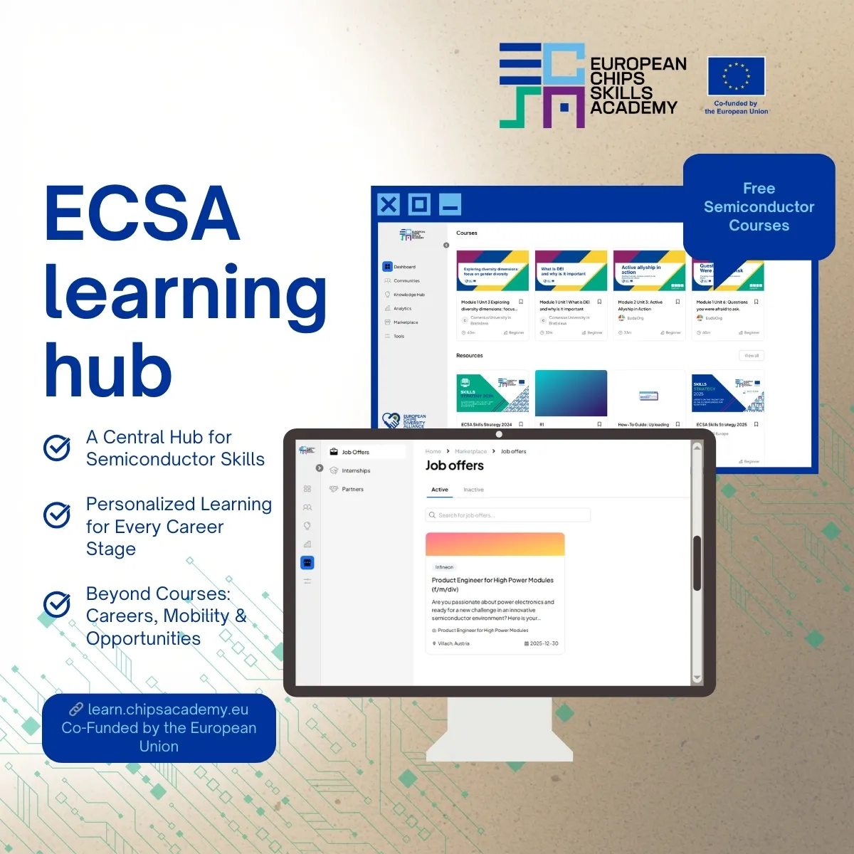
BRUSSELS — April 6, 2026 — The European Chips Skills Academy (ECSA), an European Union (EU)-funded initiative coordinated by SEMI Europe, today announced the official launch of its ECSA Learning Platform, a new digital hub with a full suite of training courses designed to support the development of semiconductor skills across Europe. With over 60 introductory to intermediate lessons, the platform brings together learning resources, collaboration spaces, and career opportunities to help students, researchers, and professionals build expertise in microelectronics and connect with the broader semiconductor ecosystem. 

Developed with input from industry and academic partners, the platform features a Knowledge Hub with curated learning materials and courses, community spaces for collaboration, and a marketplace for jobs and internships within the semiconductor value chain. Integrated learning analytics allow students to track their progress and support continuous professional development. All courses provided by ECSA partners are made entirely free for learners, supporting equal access to opportunity across Europe. 
“The launch of the ECSA Platform marks an important milestone in our mission to strengthen Europe’s semiconductor skills ecosystem and grow our workforce,” said Christopher Frieling, Director, Advocacy and Public Policy, SEMI Europe. “By bringing together education, industry insights, and career opportunities in one place, the platform helps connect talent with the skills and opportunities needed to support the future of Europe’s semiconductor industry.”

The platform is now open to students, educators, researchers, and professionals interested in exploring learning opportunities and careers within the semiconductor ecosystem. For companies and educators interested in listing employment opportunities or educational content on the ECSA Platform, please contact Victoria Cummings at [email protected]

Explore the platform: https://learn.chipsacademy.eu/

About SEMI

SEMI® is the global industry association connecting over 3,000 member companies and 1.5 million professionals worldwide across the semiconductor and electronics design and manufacturing supply chain. We accelerate member collaboration on solutions to top industry challenges through Advocacy, Workforce Development, Sustainability, Supply Chain Management, and other programs. Our SEMICON® expositions and events, technology communities, standards, and market intelligence help advance our members’ business growth and innovations in design, devices, equipment, materials, services, and software, enabling smarter, faster, more secure electronics. Visit www.semi.org, contact a regional office, and connect with SEMI on LinkedIn to learn more.

About ECSA

Launched in October 2023, the European Chips Skills Academy (ECSA) addresses skills shortages across Europe's semiconductor sector. The initiative collaborates closely with industry, academia, and policymakers to upskill, reskill, and attract new talent to the semiconductor workforce, supporting Europe's digital transition and sustainable growth. Visit https://chipsacademy.eu and connect with ECSA on LinkedIn and Instagram to learn more.

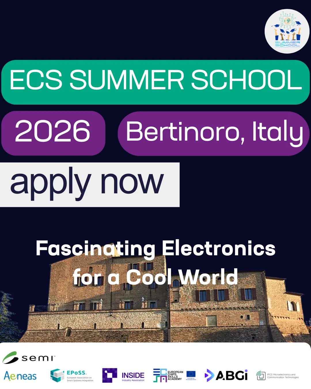
Brussels, Belgium —February 12, 2026 —The European Chips Skills Academy (ECSA), a European Union (EU)-funded project coordinated by SEMI Europe, in collaboration with industry partners AENEASEPoSS, and INSIDE, today announced that applications are open for the ECS Summer School. Taking place from 23 – 28 August 2026 at the University Residential Centre, University of Bologna, Bertinoro, Italy, the programme invites applications from undergraduate STEM students across the EU and associated countries. 

“Programmes such as the ECS Summer School are vital to motivating and developing the next generation of talent that will sustain Europe’s semiconductor workforce,” said Laith Altimime, President of SEMI Europe.

As Europe accelerates its transition to a digitally enabled future, demand for skilled professionals in microelectronics and semiconductor technologies continues to grow. The ECS Summer School offers a comprehensive, immersive learning experience designed to equip the next generation of engineers, researchers, and innovators with foundational and advanced insights into chip design, semiconductor fabrication, and embedded intelligent systems. 

“The ECS Summer School provides students with a strong entry point to acquire practical skills and form valuable connections with industry and academia,” said Patrick Cogez, Technical Director at AENEAS and ECSA lead partner for the organisation of the Summer School.

Programme Highlights
The curriculum spans four core domains of microelectronics:

  • Semiconductor Technology
  • Integrated Circuit Design
  • Digital Systems and Embedded Intelligence
  • Integration of Electronic Systems

This year’s summer school will be co-organized by ABGi and IPCEI ME/CT. Lectures, demonstrations, and interactive activities will be delivered by experts from leading universities, research institutes, and industry partners, complemented by career testimonies from engineers working in the field. 

Eligibility & Application Details
The Summer School is open to undergraduate students who will have completed at least two years of university study by the time of the event and who will still have at least one year remaining in their degree programme. Participants must be enrolled in a STEM (Science, Technology, Engineering, Mathematics) discipline at a university based in the EU or eligible associated country and possess a good command of English, as all activities will be conducted in English. 

Registration details, application requirements, and the full programme overview are available on the official ECS Summer School 2026 page. There are limited spots available, so the organisers encourage students to apply today.

About SEMI

SEMI® is the global industry association connecting over 3,000 member companies and 1.5 million professionals worldwide across the semiconductor and electronics design and manufacturing supply chain. We accelerate member collaboration on solutions to top industry challenges through Advocacy, Workforce Development, Sustainability, Supply Chain Management, and other programs. Our SEMICON® expositions and events, technology communities, standards, and market intelligence help advance our members’ business growth and innovations in design, devices, equipment, materials, services, and software, enabling smarter, faster, more secure electronics. Visit www.semi.org, contact a regional office, and connect with SEMI on LinkedIn and X to learn more.

About ECSA

Launched in October 2023, the European Chips Skills Academy (ECSA) addresses skills shortages across Europe's semiconductor sector. The initiative collaborates closely with industry, academia, and policymakers to upskill, reskill, and attract new talent to the semiconductor workforce, supporting Europe's digital transition and sustainable growth. Visit https://chipsacademy.eu and connect with ECSA on LinkedIn and Instagram to learn more.

About AENEAS

AENEAS, a not-for-profit industry association, aims to enhance the competitiveness of European industries in Electronic Components and Systems (ECS). It allows to influence RD&I policies, facilitates access to funding and offers networking opportunities. With over 550 members, it represents the full ECS value chain. Governed by a 20-member board from major companies, SMEs, and research centres, AENEAS advocates for the sector at the top European level. As a partner of the Chips Joint Undertaking, AENEAS represents the interest of its members in this tri-partite partnership between Industry, the European Commission and the participating states. AENEAS contributes to shaping and co-defining the Electronic Components and Systems Strategic Research and Innovation Agenda (ECS-SRIA). AENEAS stimulates and supports collaborative innovation to meet societal and economic challenges in a sustainable way. AENEAS is also operating the EUREKA funded programmes Xecs, PENTA and Euripides. More information: https://aeneas-office.org

High-tech systems developer Demcon has established a local presence in North America by opening a new office in San Jose, California. The Dutch contract engineering company brings decades of expertise and know-how in hardware research, design and development to the heart of Silicon Valley, where software and AI are the main focus areas.

Hardware-centric development and engineering

The brand-new office will function as a local point of contact for US customers, delivering direct project management and system architecting support. The full Demcon engineering power in the Netherlands is available for early-phase concept development, engineering, prototyping and testing, with manufacturing as an optional service. Demcon has over 30 years of experience in systems engineering for high-tech solutions, in amongst others semiconductors, photonics and quantum technology.

Demcon’s capabilities range from fundamental and essential domains such as mechanics, mechatronics, software and electronics, to crucial additional competences in multiphysics simulation, thermal management, optics & vision, and data science & AI. "With our extensive group of engineers and specialists, we have the critical mass necessary to uphold an extremely high level in all these domains", says Amir Bar, general manager at Demcon USA. "For every customer project and every challenge they bring, we pick and choose the best possible team to find the optimal solution for our customers."

As a decades-long engineering professional in the American semiconductor industry, with leading roles at Applied Materials and KLA Tencor, Bar knows firsthand what Demcon has to offer: "With the focus on software and AI, there is a shortage in hardware engineers in the US. The Netherlands, home to some of the world’s leading hardware-centric semiconductor companies, have a much stronger base in that area. Through Demcon’s US office, American customers can tap into that potential."

Expanding horizons in the American market
For Demcon, the expansion in North America is very much a strategic decision. The company is already active in the US market for 20 years. "But we see ample room for growth", says Eric Slakhorst, Vice President Demcon high-tech systems. "The country is home to many potential large customers that prefer to keep their research and development close by. Often, they are challenged by time-to-market demands and capacity constraints. We set ourselves apart by offering the possibility to outsource part of their R&D, without the obligation to give away IP, and by our fast development cycle, from feasibility study to functional prototype in 12-15 months."

As our engineers are deeply embedded in the research process with our customers, proximity is key. "To ensure an optimal result, we need to be close, as regular face-to-face interaction is vital," says Slakhorst. "That’s why we are building an engineering hub in the US to support local partners with project management and system architecting. Detailed engineering can take place in the Netherlands."