
MEMS DRIE Document Out for Ballot
By Alissa M. Fitzgerald, A.M. Fitzgerald and Laura Nguyen, SEMI
For the past few years, SEMI, working jointly with the MEMS and Sensors Industry Group (MSIG), has facilitated a joint task force that has been exploring industry challenges that span both semiconductor and MEMS/sensors manufacturing. Standards have been identified as one approach to some of the technical gaps. While the processes used to manufacture MEMS as well as Integrated Circuits (ICs) are similar, there are also unique gaps where standardization can help provide solutions that the MEMS industry can develop and adopt.
A few years ago, during a half-day workshop at SEMICON West, co-hosted by SEMI and at the time, former MEMS Industry Group (MIG), titled “Creating solutions to address common challenges facing the MEMS, Sensor and Semiconductor Industries in the next decade" was the goal to identify common denominator issues which might lead to development of new SEMI standards.
At the time, a widely held opinion was that the diversity of MEMS devices made developing standards too difficult; yet at the same time, most agreed that standards would be needed to overcome business inefficiencies and to help the MEMS industry live up to its full commercial potential.
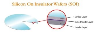
The keynote speaker at the workshop, Alissa M. Fitzgerald, drew on the history of 19th century mechanical engineering to illuminate how the creation of standards for fasteners and cutting tools was able to unify the once similarly fragmented industry of machinery. By analogy, she proposed developing standards for two frequently customized and costly items that would provide immediate benefit to both SEMI and MIG members: SOI wafers and deep reactive ion etch (DRIE) processes.
Since the integration of MSIG into SEMI, MSIG’s working groups feed the SEMI Standards Program new activities by identifying other industry challenges. The members initially focused on two areas for new standardization efforts, and two SNARFs (Standards New Activity Request Form) were submitted and approved by the members of the North America MEMS/NEMS Technical Committee Chapter following the workshop. Other areas the members are discussing for MEMS standardization are in environmental gas sensors, security, reliability, and packaging and higher integration.
The two groups have worked together on pulling together industry experts and earlier this year have successfully published their first standard on SOI wafers through this collaboration, SEMI MS12, Specification for Silicon Substrates Used in Fabrication of MEMS Devices, as mentioned in a previous article.
The second document proposed by the working group was on DRIE processes. DRIE is widely used in MEMS fabrication processes for creating high-aspect ratio anisotropic features. The optimal parameters values chosen vary widely according to the type of MEMS device and application. However, each tool type – and often each chamber – has unique recipe settings for optimum etch performance for each material. A designer typically does not know these variables before bringing a design to the foundry. These variables lead to significant costs to both the designer and the foundry, as the process must be tuned to the specific pattern and material combination, before production can commence.
Currently, the designer may not have information on how a specific tool at their foundry of choice may perform and it is common that unexpected etch results lead to missed performance target on first silicon. That is, since the designer is limited to using best known methods to achieve the desired feature sizes, the results may not meet requirements.
This Document describes test structures useful for characterizing the performance of a DRIE tool. In addition, a GDS-II file with an implementation of this etch test structure has been produced by the Task Force and is available with the ballot from the SEMI web site.
MEMS foundries can implement this test pattern, allowing them to incorporate the results into their design guidelines, eliminating the need for customers to use their design as a test pattern for the DRIE process.
The joint MEMS Task Forces and MSIG Manufacturing Working Group recently completed drafting a document on DRIE processes and the ballot is currently out for voting in Cycle 6-2020. Vote today!
Get Involved
SEMI Standards development activities take place throughout the year in all major manufacturing regions. To get involved, join the SEMI International Standards Program at: www.semi.org/standardsmembership.
For more information please visit our main Web site and current events page. If you have any questions regarding SEMI Standards activities, please contact your local SEMI Standards staff.
Standards Watch
SEMI
www.semi.org
September 10, 2020