downloadGroupGroupnoun_press release_995423_000000 copyGroupnoun_Feed_96767_000000Group 19noun_pictures_1817522_000000Member company iconResource item iconStore item iconGroup 19Group 19noun_Photo_2085192_000000 Copynoun_presentation_2096081_000000Group 19Group Copy 7noun_webinar_692730_000000Path
Skip to main content
Default Banner Image

Stanford University

SEMI is excited to recognize Amy Leong, Chief Marketing Officer and Senior Vice President, Mergers and Acquisitions at FormFactor, as the SEMI Spotlight on Women Honoree for Q1 2020!Spotlight on SEMI Women celebrates the many accomplished women who work in the global microelectronics industry. Nominees in the quarterly spotlight include women who are beacons of knowledge, leaders of organizations and initiatives, hidden heroes and innovators in our industry. They are volunteers, protectors, intellectual disruptors and activists. Learn how you can nominate a woman for Spotlight on SEMI Women.An accomplished technology executive, Amy Leong has been an invaluable leader and role model at FormFactor for over a decade. During her tenure at Formfactor, Amy has led numerous successful new‐technology adoption and customer‐penetration initiatives that have helped drive FormFactor’s market share and profitability gains. Recently, she assumed oversight of the company’s M A strategy and execution.Amy is on the advisory board of the China International Semiconductor Executive Summit (CISES) and is a committee member for both the Semiconductor Wafer Test Workshop (SWTW) and the SEMI Industry Strategy Symposium (ISS) organizing group. Amy is an accomplished, engaging speaker and has presented at industry conferences and events. As a leader and role model, she shares her experiences and lessons as a successful technology executive, coaching peers and mentoring younger women to help overcome the challenges of building their careers in the semiconductor industry. Recently, Amy broadened these efforts by spearheading the formation of FormFactor’s b3.wn Women’s Network, a group of more than 120 FormFactor employees designed to gather and solidify the community of women at FormFactor.SEMI sat down with Amy to get some insights into her success.SEMI: Tell me about your background?Leong: I was born and raised in Tianjin, China and came to United States with my family when I was 16 years old. I always liked math and science growing up, which led me to pursue an undergraduate degree in chemical engineering at UC Berkeley and then enter the semiconductor industry. My work inspired me and, with the support of my employer, I earned my masters in Material Science and Engineering at Stanford University.SEMI: How did you get into the industry?Leong: At the time of my graduation, I had been considering several career paths and industries that were open to me because of my degree. Several of my peers had already joined the semiconductor industry and told me about the amazing technology they were helping to build. Once I entered the industry, the more I worked, the more fascinated I became with the fast pace of technology and innovation. Every year there were new opportunities to innovate that came with their own exciting challenges and problems to solve. I’ve now been in the industry for 22 years and I still love what I do.SEMI: Tell me about an accomplishment you are proud of?Leong: I have been at FormFactor twice now for cumulatively over 15 years. During my current tenure of about 10 years I have worked under Mike Slessor, our CEO. What I am most proud of is my commitment to professional growth by taking on new challenges. During my time at FormFactor I have jumped on opportunities to help solve challenges in different areas of the organization. Because I pushed myself into these new challenges and experiences, I have become a versatile leader with expertise in multiple areas within the business. I remember I started in product marketing, but when a sales account manager left a need in the business, I stepped in to help the customer and found my hidden talent of customer engagement and relationship building. When we urgently needed a new supplier for product development, I drove the supplier qualification and ramp up, and learned many aspects in operations. Of course without Mike allowing and encouraging me to stretch my skills in different directions, I would not be who I am today.SEMI: Is this strategy how you ended up in the M A space for FormFactor?Leong: My role now happened through a combination of organic and planned career opportunities. M A is a key component of the FormFactor growth strategy. When Mike needed help in the new space, I was able to volunteer, and relied on the knowledge and support of our board members and our executive team in order to meaningfully contribute to our M A strategies and executionMy mentality is to always get out of my own comfort zones. If you try and fail, so what? You learn, and you improve from your setbacks. But unless you try you will never know.SEMI: You have done so much for women in the industry and at FormFactor. What drives you to do this work?Leong: There are two primary driving moments in recent years that pushed me to step up.When Ajit Manocha joined SEMI, he started raising awareness of the importance of female leaders in tackling the industry’s challenges. While I had industry visibility, I wasn’t aware that the number of women in technology shrinks alarmingly the higher up the chain of command you look. My optimistic view is that we have a nearly balanced talent pipeline at the entry-levels, and there is great opportunity for the industry to take action and change the disheartening decline in female representation by mid-career.The second moment was a personal experience. In 2015, Formfactor hired our first woman board of director Kelley Steven-Waiss. (We now have three women board members.) Having Kelley on the board and leaning on her experience when I needed guidance showed me the power of having a mentor and a role model. Having somebody there as a sounding board was extremely helpful, and this triggered me to learn more about women leadership in technology and led me to want to do more for other women who were earlier in their career.SEMI’s influence was one of the major turning points in our industry and created a clarity that was not present by putting data in front of leaders for a powerful impact.SEMI: Tell be about the process of building the network of women at FormFactor?Leong: FormFactor’s women network grew mostly through a grassroots approach. A year ago, during a QBR (Quarterly Business Review) week, I had an opportunity to get together with a group of FormFactor female sales leaders. We had a wonderful evening together, shared our experiences and learned from each other. Our conversation left an impression on us, and we decided to start a women’s networking group at FormFactor so that more women can join the conversation. We named it b3.wn – Beautiful (be confident in ourselves and kind to others) Brilliant (make smart decisions) Bold (be fearless) Women Network. These three B words are the empowering characteristics of modern women to achieve our highest happiness potential at work, home and society. We had a modest goal for the group: Provide an informal venue for employees to engage, support and learn from each other. Little did we anticipate how quickly it would gather steam. Before long, we took the initiative on the road and hosted several events at our California and Oregon sites, featuring themes that ranged from women leadership panel discussion, to FormFactor executive chats on strategies to improve work and life balance and master effective business communications. One year later we now have over 120 members.This year we are going to expand the program into Asia and Germany as well! Global expansion is an exciting step and we are getting strong support from global sites. I think people are seeing the benefits of knowing there are colleagues or friends out there that share the same sets of work life challenges and you can seek support and help from each other.We need to be the change we want to see. I hope more of us can help support women in tech and create a more inclusive work environment at your company.SEMI: What advice would you give to people looking to grow their careers?Leong: Fearlessly step out of your comfort zone. When you are far outside your element, you can discover the new skills and strengths that you didn’t know existed before. It’s a super fun adventure, but you need to expect and embrace the failures that may come along the way, learn from them, and keep going. By continuously pushing the boundaries of our comfort zone, we can expand our horizon beyond what we once thought was possible.Cristina Sandoval is manager of Workforce Development at SEMI.
Read More
SEMI has long promoted the industry collaboration that has contributed to the rise of the smart digital world we live in today. A world where data is being generated continuously by systems, gadgets, and sensors around us – often referred to as the Internet of Things (IoT). In our personal lives, most of us have smartphones, smart watches, smart TVs and smart cars, and we live in smart homes and smart cities generating huge amounts of data.In the work world, data and analytics are now influencing almost every industry including healthcare, government, financial services, construction and transportation. This data has the potential to transform our lives and make our world even smarter – if we can communicate and process this data, and use it to come up with actionable recommendations or actions. Artificial Intelligence (AI) and Machine Learning (ML) techniques have generated much excitement precisely because they offer us ways to realize the full value of data by harnessing it and transforming it into active intelligence.Data-intensive technologies are required to store, communicate and analyze data. And it all starts with innovation in microelectronics chips and systems spanning processors, memory, sensors, radios and other devices, presenting a huge opportunity to producers of these technologies. However, with Moore's Law beginning to slow, technology paths and innovation options are diverging. Companies must swiftly assess these options in order to develop competitive offerings. But the technological complexity and divergence makes it increasingly expensive or even unaffordable for many companies to track and pursue these options.The good news is that cost-effective early assessment is possible through pre-competitive collaboration that can produce new and often unexpected cross-disciplinary insights by overcoming traditional silos in industry and academia. Unfortunately, important collaborative industry platforms, such as the International Technology Roadmap for Semiconductors (ITRS), have folded, opening a collaboration gap in the global microelectronics ecosystem.As part of its mission to help companies connect, collaborate, and innovate, SEMI has built a collaborative, cross-supply-chain platform – the Strategic Innovation Platform (SIP). The goal is to provide early and comprehensive assessment of future technologies that are five to eight years away from commercialization. The assessment identifies not just technical barriers but also manufacturing and supply-chain constraints to implementing new technologies. SIP brings together the entire microelectronics ecosystem including strategic technology thought leaders, subject matter experts, technology and application developers, academia, researchers, start-ups and government. With more than 2,100-member companies spread across the global electronics manufacturing supply chain, SEMI is uniquely positioned to enable this critical collaboration. Award-Winning First ProjectThe inaugural SIP project assessed key drivers of future technologies. A key finding was that fast, efficient interconnects between devices and components are critical to the system performance important to customers and users, implying that system-level optimization is required. For data-intensive applications, interconnects have emerged as a key bottleneck for both performance and power in various circuits and systems in part because the slowing of Moore’s Law has decelerated advances in individual device performance, and in part because systems are becoming more complex, requiring heterogeneous integration.To address this challenge, SIP brought together industry experts from ASE Inc., Dow Chemical, Lam Research, Qualcomm and Xilinx to assess the future impact of interconnects for data-intensive applications. SEMI also involved Stanford University professors to collaborate on modeling and simulation. Through this unique cross-disciplinary collaboration, SIP developed a realistic model to evaluate the system-level performance of single-chip systems, as well as multi-chip systems – including traditional 2D packages, high-performance 2.5D systems that use interposers, and futuristic 3D systems. SIP also explored supply chain challenges in business continuity, manufacturability, Environment, Health and Safety (EHS) and the regulatory environment. SEMI worked with a broad range of industry partners to ensure that the model parameters accurately reflected realities on the design and factory floors to ensure usable results. Experimentation has become ever more expensive, with one industry player reporting that “it costs us $100 million to do a good experimental evaluation.” Accurate models can go a long way toward reducing the cost of technology assessment. The SIP collaboration produced key quantifiable insights including comparisons that highlight the benefits and limitations of various materials being explored for future interconnects, and of architectures under consideration for future data-intensive applications. For example, the current workhorse for artificial intelligence (AI) platforms – 2.5D technology – delivers a 4X improvement over 2D packaging but falls short of providing the orders-of-magnitude improvement that future AI/ML applications may require. These findings enable the industry to begin to identify ways to optimize 2.5D architectures, transition to 3D heterogeneous integration for performance-critical applications in the medium term, and to eventually evaluate new paradigms such as neuromorphic and quantum. The project findings were presented late last year in the form of two research papers at Electronics System-Integration Technology Conferences (ESTC) and International Microelectronics Assembly and Packaging Society (IMAPS) recently. One received the “Best Paper of the Session” award at IMAPS – a recognition that affirms the power of a collaborative platform such as SIP to produce valuable insights to address the growing technology complexity within the microelectronics industry. The microelectronics industry is on the cusp of a historic inflection point, where it could fuel the rise of emerging applications in AI/ML and IoT, and can grow into a trillion dollar industry over the next several years. More importantly, the industry is poised to help solve some of society’s most complex problems in areas including healthy living, climate change and transportation. No company can do this alone, and pre-competitive platforms such as SIP are key both to accelerating innovation through cross-disciplinary collaboration, and to reducing costs for individual companies. Please contact Tom Salmon at [email protected] or Pushkar Apte at [email protected] for more details and to get involved in future projects.Tom Salmon is vice president of Collaborative Technology Platforms. Pushkar Apte is a strategic technology advisor at SEMI.
Read More
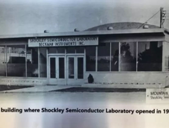
Adapted from the Computer History Museum’s “Celebrating the Birthplace of Silicon Valley” invitation. Work that sowed the seeds of the digital, hyper-connected world we know today all started in a squat, unremarkable building in Mountain View, California. Long before the structure’s foundation was laid, Santa Clara County flourished with orchards, not chips. Between the 1880s and 1940s, eight million fruit trees carpeted Silicon Valley. By 1939, San Jose, with a population of 57,651, was the largest canning and dried-fruit packing center in the world, with 18 canneries, 13 dried-fruit packing houses, and 12 fresh-fruit and vegetable shipping firms*.In 1956, silicon sprouted from new fertile ground.That’s when startup Shockley Semiconductor Laboratory, employing some of the most brilliant young minds in the business, produced Northern California’s first silicon transistor prototypes and formed the technological and cultural bedrock for today’s Silicon Valley.Fed up with William Shockley’s hard-nosed management style, eight Shockley employees – including Gordon Moore, Robert Noyce, Julius Blank, Victor Grinich, Jean Hoerni, Eugene Kleiner, Jay Last, and Sheldon Roberts – resigned in September 1957 and founded Fairchild Semiconductor Corporation. Fairchild was the seedling from which companies valued at over $2 trillion have grown and the source of the integrated circuit “computer chip” that has revolutionized our world.Now, more than 60 years later, the site of Shockley Labs, already an IEEE Historical Milestone, is being formally recognized by the IEEE and the City of Mountain View for its historical significance in a special dedication ceremony on August 15. Thanks to the efforts of many, especially developer Merlone Geier Partners, newly commissioned public sculptures – in the likeness of two early semiconductor devices and a mammoth silicon crystal monument that symbolize the work to come out of the lab – now permanently mark the site, along with various plaques that describe and commemorate the site’s history. The event’s featured speaker is Professor James F. Gibbons, former dean of engineering at Stanford University. Professor Gibbons’ first task at Stanford in 1957 was to work with Shockley and his team to transfer their knowledge of silicon fabrication to Stanford, which could in turn train future engineers for the coming boom in the semiconductor industry. He will share his personal experiences and memories of those early days. Join early semiconductor pioneers, the president of the IEEE, SEMI president and CEO Ajit Manocha and local officials on August 15 to commemorate this legendary Silicon Valley landmark. Guests are invited to enjoy a series of presentations and exhibits and view the stunning sculptures and plaques.The event is free to attend and open to the public. Space is limited so please sign up here to guarantee a seat.Location: 391 San Antonio Road, Palo Alto, California (Phase II of San Antonio Village). Parking is free.*National Park Service, Santa Clara County: California’s Historic Silicon ValleyAriana Raftopoulos is a marketing manager at SEMI.
Read More
What’s next for smarter, more connected electronics manufacturing - Part 3 The fast-maturing infrastructure now enabling analysis of exponentially larger data volumes brings the microelectronics industry to an inflection point, where the winning companies will be the first to master the use of this data to solve the industry’s emerging challenges. SEMI expands its coverage of these vital issues with a Smart Manufacturing Pavilion and three days of talks SEMICON West, July 10-12 in San Francisco. While deep learning is starting to be applied to image recognition for wafer inspection, it is also being considered for sequential pattern recognition in order to evaluate equipment parameter traces. The next emerging applications will start to use those learned patterns to predict outcomes, and then use those predictions to automate process control. One early application of deep learning is IC process development. “People don’t think of research and development as the first place to automate, but it’s where applying our digitization and simulation has first had impact,” says David Fried, Coventor vice president of Computational Products. He noted that insertion is easier in the lab than in the fab. Technology at 10nm and beyond is now so complex that companies at the leading edge must use process modeling to understand the effect of process variation on their designs. Learning cycles can now be accelerated during development by simulating 10,000 digital wafers instead of running 25 actual wafers during screening, Fried says. Applying structured analysis and machine learning to the data simplifies optimization across the 500 or more interrelated process steps. Coventor has recently introduced a statistical analysis package that aids the design and analysis of process variation experiments by using large volumes of data from its models. Fried says these models are next being used to accelerate the yield ramp in manufacturing. Digital simulation also could speed development of high-mix, lower value products While digital twins are best known for their use in complex, high value products like jet engines, the simulation technology could also enable the electronic manufacturing services (EMS) sector to reduce the time, cost and risk of developing its high mix of products. “The EMS sector’s use of digital twins will be vital for it to smooth the move of CAD/CAM digital design data for so many different products into manufacturing, and to accelerate validation testing of designs and products by doing more of it in the virtual world,” says Dan Gamota, vice president of Engineering and Technical Services at Jabil. Gamota also highlights the push for traceability from the automotive and healthcare markets, where the digital models could be used to quickly assure that the design was built exactly as specified. “In the past year, traceability has evolved from just ‘nice to have’ to ‘how to achieve,’” he adds. “Companies are expecting it, but aren’t willing to accept the cost and risk of doing it alone. We need the community to discuss realistic implementations, identify the most critical elements and bring together the ecosystem partners to build baseline reference architectures for key digital building blocks. The community also needs to assure the reliable flow of data among the electronic manufacturing segments from semiconductor to OSAT to EMS.” Predictive maintenance and virtual metrology applications could mature in next few years While predictive maintenance initially seemed a likely early application of machine learning in factories, it remains a challenge for the electronics sector. “The difficulty is that it’s not clear where to get the most bang for the buck,” says Tom Ho, president of BISTel America, noting that it may make the most sense to track the failure performance of a single expensive part, like an electrostatic chuck, since predicting the failure performance of a whole complex system like an etcher is much harder. “Collecting enough data from all failure types, including especially the rare events, is difficult unless you have a long history of a lot of tools,” adds Doug Suerich, PEER Group product evangelist. “The gain from collecting performance information from many tools across the industry could be big, but many companies still need to overcome concerns around exposing their IP.” Another big opportunity for prediction is virtual metrology – predicting the wafer outcome from the process or sensor data with enough accuracy to replace the physical metrology. “Virtual metrology is improving, and since metrology can be slow and expensive, any reduction could mean a huge potential savings,” says Suerich. “But it is still seen as too scary for many companies. Two to three years from now, companies will expand the practice from lower risk areas into processes that require more confidence in the results.” Moving beyond prediction to automated control needs digital models Once the results are predicted, the model can be used to control or automatically optimize a process and enable the system to learn by itself, usually by reinforcement learning on a digital model. The model can then independently make adjustments to optimize the manufacturing process. “Automated process development is getting close now. Instead of smart guys turning the knobs, deep learning is automating the smart tuning,” says Suerich, suggesting the industry could see widespread adoption in as little as two to three years. This type of machine learning needs a good digital model, and masses of data for learning. One approach uses human experts to build a physics-based model of the clearly understood parts of the process, then turns to deep machine learning to optimize the lesser-understood variables. The alternative, the data-first approach, runs a computer algorithm to suggest the solution purely from data, without human input, and then relies on the human to evaluate the usefulness of the results. Modeling digital twins of wafers could enable automated process control, chamber matching, and fleet matching, says Fried. If every wafer had its own virtual twin with all the upstream metrology and structural information needed to make equipment control decisions, it could feed forward that information to enable the seamless transition from one step in the process to another based on understanding their complex interrelationships. This could potentially improve uniformity across wafers and equipment, and reduce the need for metrology, he argues. Moving metrology sensors into the chamber will also require model-based algorithms to enable dynamic process control in close to real time, says Fried. These algorithms will be needed to acquire, parse, and process the data at high speed, and then to choose how to adjust the controls. “There will be a model behind collecting and interpreting the metrology data,” he notes. “That’s a really rich vein for improvements in process control.” “The end goal is to collect equipment data in real time, analyze it with AI, and send back controls to optimize manufacturing processes,” Jabil’s Gamota says. “This requires a robust architecture for communication between equipment and consistent formats for data collection and analysis. But the cost and complexity of this heavy lifting is too great for any one company to do alone. We need a consensus-based architecture for ingesting, analyzing and acting on the data.” SEMI tests data transfer protocols, benchmarks best practices SEMI is launching a smart data project to identify the various data transfer protocols needed for inter-company communications. The project will feature a proof-of-concept model in a development fab to produce verifiable results so SEMI can better understand how different approaches meet member needs. SEMI’s smart manufacturing technology communities and the Fab Owners Alliance are also benchmarking current smart manufacturing practices in the microelectronics industry to help SEMI members better understand the path forward and potential return on investment. Speakers over all three days at SEMICON West addressing these issues include Active Layer Parametrics, Applied Materials, Applied Research Photonics, ASML, Bosch Rexroth, Cimetrix, Coventor, ECI Technologies, Edwards Vacuum, Final Phase Systems, GE Digital, Infineon, Jabil, Lam Research, Osaro, Otosense, PEER Group, Qualcomm, Rockwell Automation, Rudolph Technologies, Schneider Electric, Seagate, Siemens, Stanford University, TEL, TIBCO Software. See semiconwest.org. What’s next for smarter, more connected electronics manufacturing - Part 1 What’s next for smarter, more connected electronics manufacturing - Part 2 Paula Doe, SEMI
Read More
With artificial intelligence (AI) rapidly evolving, look for applications like voice recognition and image recognition to get more efficient, more affordable, and far more common in a variety of products over the next few years. This growth in applications will drive demand for new architectures that deliver the higher performance and lower power consumption required for widespread AI adoption. “The challenge for AI at the edge is to optimize the whole system-on-a-chip architecture and its components, all the way to semiconductor technology IP blocks, to process complex AI workloads quickly and at low power,” says Qualcomm Technologies Senior Director of Engineering Evgeni Gousev, who will provide an update on the progress of AI at the edge in a Data and AI program at SEMICON West, July 10-12 in San Francisco. Qualcomm Snapdragon 845 uses heterogeneous computing across the CPU, GPU, and DSP for power-efficient processing for constantly evolving AI models. Source: QualcommA system approach that optimizes across hardware, software, and algorithms is necessary to deliver the ultra-low power – to a sub 1-milliwatt level, low enough to enable always-on machine vision processing – for the usually energy-intensive AI computing. From the chip architecture perspective, processing AI workloads with the most appropriate engine, such as the CPU, GPU, and DSP with dedicated hardware acceleration, provides the best power efficiency – and flexibility for dealing with rapidly changing AI models and growing diversity of applications.“So far it’s been largely a brute force approach using conventional architectures and cloud-based infrastructure,” says Evgeni. “But we’re going to run out of brute force options, so future opportunities lie in developing innovative architectures, dedicated hardware, new algorithms, and new software. Innovation will be especially important for AI at the edge and applications requiring always-on functionality. Training is mostly in the cloud now, but in the near future it will start migrating to the device as the algorithms and hardware improve. AI at the edge will also remove some privacy concerns, an increasingly important issue for data collection and management.”Practical AI applications at the edge where resources are constrained run the gamut, spanning smartphones, drones, autonomous vehicles, virtual reality, augmented reality and smart home solutions such as connected cameras. “More AI on the edge will create a huge opportunity for the whole ecosystem – chip designers, semiconductor and device manufacturers, applications developers, and data and service providers. And it’s going to make a significant impact on the way we work, live, and interact with the world around us,” Evgeni said.Future generations of chips may need more disruptive systems-level change to handle high data volumes with low power A next-generation solution for handling the massive proliferation of AI data could be a nanotechnology system, such as the collaborative N3XT (Nano-Engineered Computing Systems Technology) project, led by H.S. Philip Wong and Subhasish Mitra at Stanford. “Even with next-generation scaling of transistors and new memory chips, the bottlenecks in moving data in and out of memory for processing will remain,” says Mitra, another speaker in the SEMICON West program. “The true benefits of nanotechnology will only come from new architectures enabled by nanosystems. One thing we are certain of is that massively more capable and more energy-efficient systems will be necessary for almost any future application, so we will need to think about system-level improvements.” Major improvement in handling high volumes of data with low high energy use will require system-level improvements, such as monolithic 3D integration of carbon nanotube transistors in the multi-campus N3XT chip research effort. Source: Stanford UniversityThat means carbon nanotube transistors for logic, high density non-volatile MRAM and ReRAM for memory, fine-grained monolithic 3D for integration, new architectures for computation immersed in memory, and new materials for heat removal. “The N3XT approach is key for the 1000X energy efficiency needed,” says Mitra.Researchers have demonstrated improvements in all these areas, including multiple hardware nanosystem prototypes targeting AI applications. The researchers have transferred multiple layers of as-grown carbon nanotubes to the target wafer to significantly improve CNT density and have also developed a low-power TiN/HfOx/Pt ReRAM. The low-temperature CNT and ReRAM processes enable multiple vertical layers to be grown on top of one another for ultra-dense and fine-grained monolithic 3D integration. Other speakers at the Data and AI TechXpot include Fram Akiki, VP Electronics, Siemens; Hariharan Ananthanarayanan, motion planning engineer, Osaro; and David Haynes, Sr. director, strategic marketing, Lam Research. See SEMICONWest.org.Paula Doe, SEMI
Read More
What’s next for smarter, more connected electronics manufacturing - Part 2The fast-maturing infrastructure now enabling applications for big data and artificial intelligence means disruptive change not just at individual companies but also in data connections among companies across the microelectronics manufacturing value chain. SEMI checked in with some leading players on the changes they see coming in the next several years for this article series. The trade group is expanding its programming on smart manufacturing to address these industry-wide developments at SEMICON West, July 10-12 in San Francisco.“The ramp of EUV, and the smaller geometries and smaller process margins, will drive an exponential increase in the amount of metrology data to manage,” says Neal Callan, ASML vice president, Silicon Valley. Callan notes that moving to multibeam e-beam inspection will increase data volume from megabytes per second to gigabytes per second and from thousands of data points to millions of data points. “The process is so tight and the margin so small that stochastic variation, or noise, becomes more dominant – at least it’s noise until we can learn to understand and control it. And understanding and controlling this variation will be key to delivering 5nm patterning,” he says.Single-beam e-beam inspection is already driving large increases in data as engineers extend the slow technology to broad, high-speed defect metrology applications by more intelligently instructing the system where to look for problems. Callan says ASML is now using the scanner data on wafer focus, alignment and leveling. The company is also using the computational lithography model from the design to identify the smallest process windows in the pattern that are most likely to see problems. The model then quantifies the number and significance of those instances.“The collection of all this diverse data means that tools will need to be plug-and-play so all tool data is instantly available to all systems and software,” says Doug Suerich, PEER Group product evangelist. “We need tools that can be discovered automatically by the network so it can start slurping up data immediately. The adoption of the Interface A (EDA) standard is accelerating and fabs are starting to ask for it. The proliferation of sensors also needs to self-discover. If you are going to add thousands of new sensors into a facility, you can’t afford a time-consuming integration process.”“We are now seeing that engineers are greedy for more data – if they can get the data, it’s becoming a need-to-have,” adds Tom Ho, BISTel America president. “Getting more data from more sensors, from the sensors on the tool that are not being fully utilized, and from untapped data sources like vibration is another big coming opportunity.” Process complexity drives demand for feed-forward between silos with computational models ASML co-optimizes its scanner process with etch and reticle process steps. Source: ASML In addition to the drive for trace-back of data, the increasing complexity of interrelated processes is also driving demand for feed-forward of data. “Feed-forward is becoming more important,” notes Ho. He points to the example of 3D NAND features, now getting so deep that identifying the layer being measured is a challenge unless the signal at the step before can be recognized. “We need partnerships with our peers to understand how to take advantage of the sensors they use, integrate them with our data, and then feed-forward corrections to the other systems,” concurs Callan. “To drive the best CD uniformity and overlay, we need to co-optimize litho and etch,” agrees Henk Niesing, ASML director of product management. He notes that the company is working with etcher makers to measure the overlay and CD, decompose the finger prints, and then use models to steer automated control that best adjusts both the scanner and the etcher. ASML is also working with Zeiss on co-optimization between the scanner and the reticle to make even higher-order corrections by locally modifying the reticle.These higher-order corrections, applied on each exposed field, drive the need for even more data, and at higher speed but without higher cost, notes Jan Mulkens, ASML senior fellow. These corrections increase demand for computational metrology, which combines various metrology sources with physics and deep learning models trained on real data to predict and control process results in real time. “We’re working on computational metrology to ideally use all the knobs we have in the fab,” he says. So far this effort has largely involved linking data between two companies. More consistent data formats would enable data exchange to be extended to more companies. “The software versions also need to be managed for upgrades so they still match after one party updates the system on its tool,” notes Niesing. Speakers on these issues of smart manufacturing and data handling at SEMICON West include Active Layer Parametrics, Applied Materials, Applied Research Photonics, ASML, Cimetrix, Coventor, ECI Technologies, Edwards Vacuum, Final Phase Systems, GE Digital, Infineon, Jabil, Lam Research, Osaro, Otosense, PEER Group, Rockwell Automation, Rudolph Technologies, Schneider Electric, Seagate, Seimens, Stanford University, TEL, TIBCO Software. See semiconwest.org.What’s next for smarter, more connected electronics manufacturing - Part 1What’s next for smarter, more connected electronics manufacturing - Part 3Paul Doe, SEMI
Read More
What’s next for smarter, more connected electronics manufacturing - Part 1The fast-maturing infrastructure now enabling applications for big data and artificial intelligence means disruptive change not just at individual companies but also in data connections among companies across the microelectronics manufacturing value chain. SEMI expands its smart manufacturing program with a Smart Manufacturing Pavilion with displays and three full days of talks to address these industry-wide developments at SEMICON West, July 10-12 in San Francisco.Autonomous autos’ demand for zero-defect systems and 100 percent traceability back to the manufacturing data for each die is driving a push to traceability across the chip sector. “Far more chips are being used by the automotive sector, and its very different requirements are driving demand for traceability,” says Tom Ho, president of BISTel America. “Our chipmaker customers are looking for traceability solutions and the trend is the same in backend packaging and assembly – automotive applications are driving the sector to traceability.”Traceability is also driven by the growth of systems in a package as fabless chipmakers look to connect back to the packaging companies’ fault analysis labs and die interconnect history to diagnose and fix the cases where known-good die are failing in the system, adds Mike Plisinski, CEO of Rudolph Technologies. Plisinski adds that makers of consumer products like phones that can also see harsh conditions are demanding higher quality and traceability as well. The electronic manufacturing services (EMS) sector also must establish an architecture for traceability to collect critical manufacturing-related data and to interface with OSATs and semiconductor fabs. The reason is that EMS companies are adding traditional OSAT processes such as assembly of products with bare die and complex optics modules requiring clean rooms. “A unified sand-to-smart-phone smart manufacturing roadmap should be established,” says Dan Gamota, vice president of Engineering and Technology Services at Jabil. “We need to identify protocols for manufacturing data communications that can be adopted across the supply chain.”To enable smart manufacturing, vendors need to collaborate on getting their production equipment to interoperate and support factory analytics and data management systems. Source: SEMI One big challenge, of course, is how to format this diverse data so it can be linked and used by various supply chain stakeholders. “Smart data needs to be contextual and it needs data standards across the supply chain so it’s easy to link from the front end to the back end, follow common lot IDs front and back end, and have a way to map streaming data from sensors to a discrete lot ID,” notes Ho. New approaches to metrology, analysis and test that increasingly exploit machine learning on simulations will also be needed to help predict which die and connections that test well now may fail in the future as conditions change.Another issue is how to securely share the needed data across companies without jeopardizing IP. “On the equipment side we collect data across customers on how the tool is running to improve the equipment,” notes Neal Callan, ASML VP Silicon Valley. “Next we need to integrate performance and reliability data that today is not as well shared.”The other big hurdle is how to pay for data sharing. “The challenge is that the final manufacturers reap the benefit of traceability, but since they expect their suppliers to deliver good die, they don’t want to pay more for it,” notes Plisinski. He suggests that over the next two to three years, traceability and predictive fault prevention will become the norm as the automotive sector is compelled to invest in it to assure safety. Meanwhile, fabless companies will face so much complexity in integrating different die from different suppliers in SiP that they will no longer be able to afford to simply use the cheapest supplier, potentially driving a fundamental shift in relations and division of labor among fabless chipmakers, OSATs and fabs. Standards extend across supply chainSEMI member committees are collaborating to build the infrastructure to enable these developments. Standards committees are updating standards for higher bandwidth data exchange and extending semiconductor-like vertical and two-way horizontal equipment communication standards to flow shops to enable assembly players to optimize and trace back results across players. The SMT/PCBA community is integrating its smart manufacturing work into SEMI standards, and the SEMI A1 standard was a key reference document in the development of the Japan Robotics Association’s Equipment Link Protocol.Speakers addressing these issues at SEMICON West include Active Layer Parametrics, Applied Materials, Applied Research Photonics, ASML, Bosch Rexroth, Cimetrix, Coventor, ECI Technologies, Edwards Vacuum, Final Phase Systems, GE Digital, Infineon, Jabil, Lam Research, Osaro, Otosense, PEER Group, Qualcomm, Rockwell Automation, Rudolph Technologies, Schneider Electric, Seagate, Siemens, Stanford University, TEL, TIBCO Software. See semiconwest.org.What’s next for smarter, more connected electronics manufacturing - Part 2What’s next for smarter, more connected electronics manufacturing - Part 3Paula Doe, SEMI
Read More