downloadGroupGroupnoun_press release_995423_000000 copyGroupnoun_Feed_96767_000000Group 19noun_pictures_1817522_000000Member company iconResource item iconStore item iconGroup 19Group 19noun_Photo_2085192_000000 Copynoun_presentation_2096081_000000Group 19Group Copy 7noun_webinar_692730_000000Path
Skip to main content
Default Banner Image

Intel

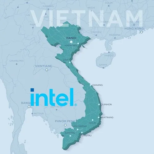
A 500,000 ft2 (~47,000 m2) state-of-the-art cleanroom facility still towers as the largest U.S. high-technology investment in Vietnam 10 years after starting operations in Saigon High Tech Park in District 9, Ho Chi Minh City. The structure built by Intel Products Vietnam (IPV) on the back of a $1 billion investment is the largest assembly and test manufacturing facility (ATM) in the Intel assembly and test network. IPV turns out products that are helping power cutting-edge applications along with the next wave of semiconductor industry growth as it homes in on 5G, Internet of Things (IoT), desktop and mobile. And it has been a boon to the local economy, generating more than 5,000 high-skill jobs across a number of assembly and test disciplines since launching operations in 2010. It has also contributed to over US$37 billion in exports from 2010 to 2019, accounting for over 60% of Saigon High-Tech Park’s annual export values in 2019. With its vision “to create the future of Intel and Vietnam,” Intel continues to be a strong long-term partner in Vietnam. I recently spoke with Kim Huat (KH) Ooi, vice president of Manufacturing and Operations and General Manager at Intel Products Vietnam (IPV), about the facility’s vital role in Intel’s overall manufacturing operations, its support for the E E ecosystem in Ho Chi Minh City, and measures it has implemented to reduce the impact of the COVID-19 pandemic on the facility and protect employees. Ooi leads and manages the site to support Intel’s business in Vietnam. His responsibilities include overseeing factory operations and employee relations; enriching the Intel image and brand; building strategic relationships with communities, media, governments, and local authorities; and working with the industry ecosystem and government. IPV employees celebrate Intel’s 50th anniversary in 2018. Ng: How does IPV campus complement the rest of Intel manufacturing sites and be nearer your customers and supplier base?Ooi: Intel Vietnam is an important part of Intel’s manufacturing presence worldwide. IPV has been operating for nearly 14 years in Vietnam and has celebrated multiple milestones along the way. As a site, we have matured and grown over the years. In March this year, we celebrated a proud milestone – the rollout our 2 billionth unit – that reflects the value of IPV to Intel Corporation as these Made in Vietnam products support its customers worldwide. One of our philosophies is to work with and grow local ecosystems in countries where we operate. In Vietnam, Intel has been offering technical and managerial expertise to many local suppliers in Vietnam to help them expand their business and services to other foreign direct investment (FDI) customers in the industry. Over the past 10 years, Intel’s supplier list has grown 10-fold from 20 in 2010 to about 180 suppliers in 2020.In today’s world of fast-changing consumer preferences and expectations, we need to help drive development of the latest products and technologies to support strong customer demand and new product portfolios such as 5G. To support evolving customer requirements, our workforce frequently upgrades its skills to work on new products and technologies.Intel as a company is also evolving as it transforms from a PC-centric to a data-centric organization, a shift behind the more than US$70 billion in record revenue Intel posted in 2019. Intel’s data-centric business accounted for more than half of that revenue. IPV plays a key role in Intel’s expansion into new market segments.Ng: What are the key differentiating elements (talent, tax, technology, trade, EHS) in Vietnam that have been instrumental in supporting the E E ecosystem in Ho Chi Minh City?Ooi: Vietnam’s stable political environment and increasingly liberalized trade and investment policies are great for businesses. The region’s young, talented workforce is also one of many competitive advantages that enables it to attract foreign investment. Intel’s announcement to invest in Vietnam in 2006 has played a large part in helping put Vietnam on the map of the global IT and semiconductor industry. The news helped attract industry suppliers and service providers, bolstering Vietnam’s economy and creating jobs. The Vietnam government also figured prominently in sparking the boon by establishing the right policies and incentives to attract foreign investment. Since starting operations, we have seen significant improvements in infrastructure such as roads, ports, airports, broadband and power supply. Vietnam’s standing in the global business community is even stronger today after the government successfully combatted the COVID-19 pandemic early on and introduced policies to help businesses restart operations. We expect all these factors to continue to make Vietnam an attractive relocation target for companies around the world. Ho Chi Minh City People’s Committee Vice Chairman Mr. Duong Anh Duc (center) visited Intel Vietnam to tour the state-of-the-art facility. Ng: What measures have you implemented to reduce the impact of the COVID-19 pandemic and protect employees? Ooi: COVID-19 has taken the world by storm and changed the way we work and live in many ways. It has unquestionably pushed the world to build stronger partnerships among individuals, organizations, businesses and communities. Intel’s manufacturing operations have continued to run at full capacity. Since the outbreak emerged, we have strictly followed required Intel safety measures as well as the Vietnam’s health guidelines. We have also implemented a number of other safety initiatives and protocols to ensure our business runs smoothly. We’re doing everything possible to ensure the well-being of our employees and help them better respond to the pandemic.In coordination with our strategic partners, we have been donating thousands of Personal Protective Equipment (PPE) to the Fatherland Front and Department of Health (DoH) since early March. Recently, in partnership with AmCham Vietnam, Intel donated an imported ambulance with built-in essential equipment to the Ho Chi Minh City 115 Emergency Center. Intel has also teamed with Saigon Hi-Tech Park management to donate two ventilators and N95 masks to DoH.Our employees are also helping out by donating to Vietnam’s Coronavirus Donation Matching campaign. We collected US$13,000 from Intel employees and included matching funds from Intel Foundation to support three non-profit organizations (NPOs) – Saigon Children’s Charity, Kidspire Vietnam and Teach for Vietnam. All told, Intel Products Vietnam has donated US$200,000 to COVID-19 relief efforts, demonstrating our long-term commitment to communities where we operate. Intel Products Vietnam teamed with AmCham Vietnam to donate a fully equipped ambulance to Ho Chi Minh City’s 115 Emergency Center, demonstrating IPV’s long-term corporate social responsibility commitment. In early May, Intel unveiled our 2030 Corporate Strategy and goals to accelerate progress against the world’s critical challenges and help drive positive global outcomes. Part of our 2030 goals, our RISE (Responsible, Inclusive, Sustainable, Enabling) strategy focuses on the company’s commitment to its corporate social responsibility (CSR) initiatives to create a more responsible, inclusive, safe and sustainable world through technology and collective action. IPV has also committed to implementing the RISE strategy in Vietnam with local community initiatives and technology interventions. Bee Bee Ng is president of SEMI Southeast Asia.
Read More
Tracking and quickly diagnosing COVID-19 infections, working from home and telemedicine recently came into sharp focus as technology executives and other subject matter experts from microelectronics heavyweights recently gathered for the first-ever virtual SEMI CTO Forum to explore how the microelectronics industry and their own companies can leverage future technology trends to drive growth. Themed Intelligent Medtech and Wearable Technologies, the forum drew CTOs from ARM, Babblelabs, Brewer Science, Dell, Dow/Dupont, E-Ink, Hewlett Packard Enterprise, Intel, Lam Research, KLA, Microchip, ON Semiconductor, Qualcomm, Tokyo Electron, Ulvac, Veeco and Xilinx. The event is designed as a strategic driver of pre-competitive innovation. Following are key takeaways from the forum. Microfluidics Promises to Speed COVID-19 Diagnosis More than 240 companies worldwide are developing microfluidics solutions to improve diagnosis and treatment of COVID-19 and other conditions, said forum speaker Dr. Kurt Petersen, a member of Band of Angels, Silicon Valley's oldest angel investment group, with an illustrious background1 in technology. And their innovations are bearing fruit. Cepheid, a company founded by Dr. Petersen, has developed a disposable microfluidic cartridge, Xpert Xpress SARS-CoV-2, used by doctors to swab the inside of a patient’s mouth. Highlighting the vital role of MEMS in medical electronics, the tiny powerful devices are behind a test that can detect COVID-19 infection in under 40 minutes. Dr. Petersen also cited a few examples of implantables and injectables under development, including: In vivo chemical sensing: Profusa developed a continuous glucose monitoring sensor via an optical patch. Glaucoma pressure monitors: Injectsense built a silicon chip the size of a grain of rice that is embedded in the eye to measure eye pressure. Retinal implants: Second Sight implanted a 60-electrode array chip that projects images onto the retina to improve vision. Microelectronics Takes Aim at Battling COVID-19 The event’s CTO roundtable, a platform for discussing societal and technology issues, revealed microelectronics technology will likely give rise to solutions for combatting pandemics and new business opportunities both in the short and long run. Areas of the greatest interest included: Tracking and Security: Infection tracking accuracy is key to limiting the spread of viruses yet comes with inherent privacy and security challenges. The consensus view of the executives was that developing trusted hardware capabilities is critical for adoption of accurate infection-tracking technologies. Remote Operation: Executives expect working from home or the use of telehealth to continue building momentum long after pandemic. To give staying power to the remote communications at the heart of these trends, microelectronics ecosystems will need to boost compute performance, both at the edge and in the cloud, while increasing bandwidth to enable applications such as augmented reality/virtual reality (AR/VR), artificial intelligence (AI), machine learning and advanced data analytics. Edge intelligence: The challenge of remote communications spans both people and the Internet of Things (IoT). Questions persist about how hundreds of billions of sensors will connect to the cloud and how much power they will consume. The need to push computing to where data is generated – at the edge – is rising and the necessary underlying technologies will only come by combining various forms of distributed computing and analytics. The microelectronics industry’s ability to seize these opportunities will only be possible with huge strides in innovation, raising concerns among the CTOs about the financial viability of cutting-edge devices because of increasing device complexity and R D costs. Technology partnerships and collaborations – an area where SEMI is contributing and will continue to expand its efforts as it works with the CTO community – will be critical to containing R D costs. SEMI will help the executives identify and mobilize the resources key to future innovation. Improving Home, Work Productivity and Experiences Key to AR Adoption Smart wearables also offer great promise. In just over a decade, AR and VR have grown from science fiction to practical uses such as AR applications for smart contact lenses, said Dr. Mike Wiemer, Co-Founder and CTO of Mojo Vision2. Dr. Wiemer said that while many AR applications remain under development, the technology will only see widespread adoption once it starts to improve productivity and efficiency at home and work and the quality of other experiences. The smart augmented reality contact lens developed by Mojo Vision is a step in that direction. The product’s built-in display gives users timely information about everything they see while remaining invisible by packing 70,000 pixels into a space smaller than a half a millimeter across, making it the smallest and densest dynamic display ever made. The contact lens is powered by an ARM-based processor, with later versions adding an image sensor, eye-tracking sensors and a communications chip. SEMI thanks EMD Performance Materials and Telit for sponsoring the CTO Forum. For more information on the CTO Forum and SEMI’s Smart Data-AI initiative, please sign up on our webpage. 1 Dr. Kurt Petersen is a member of the National Academy of Engineering, an IEEE Medal of Honor winner, and a Life Fellow of the IEEE for his contributions to the commercialization of MEMS technology. 2 Dr. Wiemer also co-founded Solar Junction, where he led technical teams to two world records in solar cell efficiency (43.5% and 44%). He also has patents and papers in Semiconductor Devices Applications, Silicon Photonics, Materials Integration, Lasers, Solar Cells, Solar Systems, and Analog Circuits. Tom Salmon is Vice President of Collaborative Technology Platforms at SEMI. Pushkar P. Apte, Ph.D., is Strategic Technology Advisor for the Smart Data AI Initiative at SEMI.
Read More
Humanity has survived almost unimaginable challenges over the past 5,000 years of documented human history. From war, famine and natural disasters to the first global pandemic in the last 100 years, more often than not, people have relied on one another to survive and thrive again. As the industry association representing the global microelectronics industry, SEMI has similarly made collaboration and community integral to the fabric of its organization. From helping members to succeed through the COVID-19 pandemic to facilitating member-driven industry standards around environmental health and safety, materials, and manufacturing capabilities, this approach shows members that standing together is better than standing alone.On the eve of the 50th annual SEMICON West (July 20-23, 2020) — the first virtual edition in SEMI’s history — I spoke with SEMI’s vice president of technology communities, Michael Ciesinski, about the role of SEMI in tackling big challenges through an active member community intent on solving problems through collaboration.SEMI: How long have you worked with SEMI and in what capacity?Ciesinski: In January 2016, I started my second tour at SEMI when FlexTech, the industry consortium I’d been leading, became SEMI’s first strategic partner. Nearly two years into that role, SEMI President CEO Ajit Manocha asked me to form Technology Communities to engage members with common interests. After FlexTech, we brought on the Fab Owners Alliance, then MEMS Sensors Industry Group (MSIG), and later the Electronic System Design Alliance (ESD Alliance).SEMI now has more than 20 communities in all, including Smart MedTech, Smart Data AI, Smart Manufacturing, Electronic Materials, and Integrated Packaging, Assembly and Test.SEMI: What is your role with Technology Communities — and how do members stand to benefit?Ciesinski: The leadership of Technology Communities ensures that SEMI’s benefits and services align to our members’ interests so we can provide member benefits that matter most. This spans forming communities where people hold common interests (e.g., advanced packaging) to facilitating standards that will promote intelligence in manufacturing (e.g., data standards for AI and machine learning) as well as providing R D funding.I’m especially proud that over the past three years, SEMI has brought more than $40 million in R D funding to our members, with most grants in the $500,000-$1 million range. We’ve been especially successful in securing funding in flexible hybrid electronics (FHE) through U.S. Army Research Laboratories (ARL), a model we first developed through FlexTech.Two recent recipients of FHE funding, GE Research and ITN Energy Systems, show how the grants are spawning partnership opportunities among commercial enterprises, R D organizations and universities. In developing lightweight, non-invasive wearables, including a human-performance sweat-monitoring patch that remotely analyzes sweat to detect hydration levels and other vital signs, GE Research is using key components such as sensors and lightweight batteries in its designs.ITN Energy Systems designed a flexible all-solid-state lithium battery that’s printed on light, flexible substrates to power small and incredibly thin applications.Universities are also benefiting by plugging into the SEMI ecosystem. In fact, 40-50 percent of funded projects are seeding commercialization by universities. This is another validation that SEMI’s collaborative, community approach to microelectronics is working.SEMI: Position, Timing and Navigation (PNT) is another hot area where SEMI has secured ARL funding. What makes this funding different and why is it important?Ciesinski: The PNT grant makes ARL funding available to the MEMS Sensors Industry Group (MSIG) members through SEMI for the first time. If you’ve ever lost GPS signal while coming out of a tunnel, you know how frustrating that is. For us, that’s an inconvenience, but for a healthcare worker in a remote location who’s waiting for a delivery of medication by drone, it could be life-critical. While that’s just one example of why we need PNT to operate when GPS isn’t available, I can imagine dozens of other important dual-use cases, including autonomous driving.SEMI: How else do Technology Communities benefit under SEMI?Ciesinski: Technology Communities need access to diverse resources to spur continuous innovation. Electronic Materials Group participants, for example, need to stay informed on regulations coming out of Asia, the U.S. and Europe that may affect their businesses. Where else other than SEMI can like-minded stakeholders congregate with people up and down the supply chain to determine whether industry-wide action is needed on regulation?SEMI: What is the importance of SEMI’s global footprint?Ciesinski: I’ve worked with many associations and managed major industry consortia. The clear advantage of SEMI is our global footprint. And that’s vital because microelectronics is a global industry involving a multitude of stakeholders that play essential roles in the supply chain.Let’s say you want to discuss EU regulations on hazardous chemicals. Rather than decipher these complexities alone, you can pick up the phone to speak with someone on SEMI’s European team to learn what’s critical.What if you’d like more information on the 20-plus new fabs that are going up in China? You can explore that question with our SEMI China or SEMI Industry Research and Statistics teams.SEMI: How has SEMI evolved over the years?Ciesinski: SEMI has a long history of providing what the industry cares about. We started in trade shows and pivoted to industry standards. We began with small silicon wafers and wafer carriers, and now within the span of 50 years we’re working on data-format standards that will support the application of AI and machine learning (ML) in the semiconductor industry.While highly varied today, data-format standards will help component manufacturers refine processes to create more efficient solutions. This ARL-funded program, which pairs SEMI members with the grant recipient, Cornell University, may offer dramatic gains in the productivity of semiconductor manufacturing.SEMI: How does SEMI’s approach to COVID-19 reflect core values of collaboration and community?Ciesinski: Together with Ajit Manocha, CMO Terry Tsao and other team members at SEMI, we pulled together a task force to help SEMI members navigate the pandemic.We tapped two existing groups, Environment, Health and Safety (EHS) and Information Technology Leadership (ITL) from the start, documenting their strategic and tactical approaches to help all members through the COVID-19 resource section of our website. The EHS section provides tips on facilities and meetings, employee policies, business travel and communications, while the ITL section lists insights on computing hardware for staff, licensing, networks, security and employee policies.Our EHS leadership team, which includes Entegris, Axcelis, Versum, and Intel, immediately started sharing best practices for sanitizing facilities. As a result of team meetings, SEMI EHS shared best practices on keeping the workforce remote and guidelines for returning people to work safely. From securing PPE and safeguarding employees and visitors by performing thermal scanning to outlining communications around potential employee exposures, EHS has provided meaningful resources for the benefit of all members.SEMI also took immediate steps in the area of advocacy. Our advocacy team in Washington, D.C., together with regional SEMI presidents around the world, have ensured that semiconductor facilities were and still are considered essential businesses in the U.S., Europe and Asia. That’s because microelectronics are foundational to fighting the pandemic.Microfluidics are critical to the Reverse Transcription (RT) Polymerase Chain Reaction (PCR) tests most commonly used for COVID-19. Sensors are embedded in the pulse oximeters that allow patients and healthcare professionals to monitor a vital rubric: oxygen saturation level. If oxygen saturation level drops into the low 90 percentiles or below, it may be time to go to the hospital for treatment.Microcontroller units are essential components in a wide range of hospital equipment, including the ventilators that may make the difference between life and death in the most seriously ill patients.SEMI: How can the ingenuity realized through microelectronics continue to help us tackle other big problems? Ciesinski: We have MEMS and sensors to thank for distributed intelligence, giving us the ability to put sensors anywhere, locally based in the field or in the packaging house.Food production is a prime example. Leveraging miniaturized wirelessly connected sensors, we can trace food through the entire production lifecycle, from the seed in the ground to the food in the warehouse and, ultimately, to the product that lands on the table.From larger enterprise such as IBM Food Trust to small startups, we’re using MEMS and sensors to improve crop yields so we can feed a human population that’s growing each year.There’s a sustainability piece as well. We’re using MEMS and sensors to reduce the amount of fertilizer or other nutrients or chemicals in the soil. That’s good for the environment and for the agricultural workers who labor in the fields.MEMS and sensors can also condense the time it takes to perform a specific task, conserving human resources.SEMI: Where do you think SEMI will go in the next decade?Ciesinski: Ten years from now, I believe we will still have our global footprint in place. I expect it will expand, particularly in Asia.We may also expand into new areas such as Latin America and Central America, which would provide at least two major benefits: People working in microelectronics would, I hope, have access to better quality of life. And diversifying the supply chain would allow nations and regions to have more control over the products they need, from PPE to medications, which may help us to better manage through the next pandemic.I am also hopeful that SEMI will be on the leading edge of helping our members communicate in much different fashion from what we have today. We’re already expanding beyond the paradigm of in-person meetings for standards meetings and conferences. As we move forward, I think we’ll see a hybrid solution to doing business, combining in-person meetings with virtual conferences and digital content that’s available 24/7.Whatever changes we see in SEMI, I’m confident that we will continue to see a global footprint in an industry association that prioritizes connections among members.Engage in the SEMI experience at upcoming SEMICON WestRegister today to hear from keynote speakers such as environmental advocate and former U.S. Vice President Al Gore, futurist and author Steve Brown, and IBM Research senior vice president and director Dr. John E. Kelly III, and Lea Gabrielle, special envoy of the Global Engagement Center for the U.S. State Department, at SEMICON West , July 20-23, 2020. Content will be live streamed and available on-demand. Michael Ciesinski is vice president of Technology Communities for SEMI, the global microelectronics industry association, appointed in August 2018. At SEMI, he directs activity for more than 20 industry groups, oversees the association’s R D funding program, and develops new technology initiatives to serve SEMI’s 2,400 members. Prior to re-joining SEMI, Ciesinski was president/CEO of FlexTech Alliance, an industry consortium focused on new methods of creating electronics. From 1995-2008, Ciesinski served in a similar role at the U.S. Display Consortium (USDC), a private/public partnership chartered with building the infrastructure for electronic display and flexible electronics manufacturing. Both FlexTech and USDC annually sponsor multimillion dollar technology development programs and provide industry technical, financial and market services. Ciesinski is a graduate of the University of Albany, NY, and a former member of the Dean’s Advisory Committee at California Polytechnic State University.Maria Vetrano is a PR consultant at SEMI.
Read More
Last year the industry posted another remarkable double-digit revenue growth year. IC shipments eclipsed one trillion units for the first time and continued to enable an ever-expanding array of silicon intensive-applications.2018 was also a pivotal year of transformation at SEMI. Setting our sights firmly on building more value for SEMI members, we doubled down on priorities I established this time last year. We advocated intensively on global trade policies, industry talent needs, and critical environment, health and safety (EHS) concerns. To underpin our efforts around talent, we took the bold step to reinvigorate the industry’s identity with a dynamic image campaign. Above all, we targeted critical industry-wide issues to help us realize the ambition of becoming a trillion-dollar industry in the next decade. Workforce DevelopmentRedefining our approach to talent development in 2018 was and remains a top priority. A diverse, highly skilled workforce is crucial to the industry’s ability to innovate. Last year we ramped up a number of SEMI High Tech U (HTU) programs to inspire young people and attract them to careers in high-tech manufacturing. To date, more than 130,000 students have been touched by HTU – through student or teacher programs.Over the past year, we designed a new university outreach program and established partnerships with 100 institutions. We established Workforce Pavilions at SEMICON events in Southeast Asia, the U.S., Taiwan, Europe and Japan for students to explore career opportunities and meet with recruiters. We thrilled at seeing sponsors hire young talent at SEMI events. This year, all SEMICONs worldwide will feature Workforce Pavilions.SEMI also formalized its commitment to Diversity and Inclusion (D I) with the establishment of a D I council to shape new programs including the recently launched Spotlight on SEMI Women. To localize and fully optimize our D I programs, we established regional workforce councils in every region we serve. We unveiled the SEMI Mentoring Program to support students and young professionals on this journey by facilitating one-on-one mentoring relationships with industry professionals. Hundreds of mentees have enrolled. But we still need more mentors. I urge you to join the program. During the year, SEMI also expanded its workforce staff and developed a comprehensive workforce strategy with programs that engage students as early as elementary school and inspires them through high school and college. The program provides pathways to professional careers, building a pipeline to fill the short-term and long-term talent needs of the industry. Industry Image CampaignAs we developed the comprehensive workforce development program, we knew we had to refresh the industry’s image and appeal to the next generation through contemporary media and communications channels. So we recently launched a bold, innovative campaign to raise industry awareness and attract students and recent graduates to careers in semiconductor manufacturing.Our You’re Welcome campaign is a novel, creative approach that blends entertainment, media and storytelling to excite students about the industry. The campaign went viral immediately and within weeks had more than 5.5 million social media impressions and 2.3 million video views.Trade Policy AdvocacyRising trade tensions between the U.S. and China catapulted global trade policy to the forefront of industry concerns in 2018. Since the tariffs have taken force, semiconductor companies have faced higher costs, greater uncertainty, and difficulty selling products abroad. The tariffs have forced many SEMI member companies to pause or rethink their investment strategies.SEMI quickly engaged U.S. policymakers and provided resources for SEMI members. We formed a member trade task force, staged trade compliance seminars in China, and convened meetings with over 110 U.S. congressional, agency and administration officials, and provided testimony on the importance of the free trade to the industry.SEMI continues to educate policymakers about the critical importance of free and fair trade, open markets, and respect and enforcement of IP for all players in the global electronics manufacturing supply chain. As part of this initiative, we distributed “10 Principles for the Global Semiconductor Supply Chain in Modern Trade Agreements” and encouraged their adoption in various trade negotiations. These principles outline the primary considerations for balanced trade rules that benefit SEMI members around the world, strengthen innovation and perpetuate the societal benefits of affordable microelectronics.Environment, Health and SafetyEnvironmental regulations are proliferating globally even as advanced semiconductor manufacturing technology relies increasingly on a host of new materials. With dozens of new fabs and fab line upgrades, our industry must align on best practices, sensibly respond to materials restrictions, and renew efforts toward sustainable manufacturing.That’s why the revitalization of SEMI EHS efforts became another priority in 2018. Two months ago, we hosted the inaugural EHS Summit at SEMI Headquarters. Fully, 70 EHS professionals and company executives met to form the basis for the future SEMI EHS program.The Year AheadDespite a softening in the market, compounded by Apple’s first-ever announcement of a revenue decline in 16 years, a geopolitical whirlwind on trade and an extended shutdown of much of the U.S. government, the future is bright.At SEMI’s annual Industry Strategy Symposium (ISS 2019) in Half Moon Bay, Calif. in early January, the sense of optimism was palpable. In her keynote address, Dr. Ann Kelleher, Sr. VP and General Manager, Technology and Manufacturing Group, at Intel, observed that data is powering the fourth industry revolution and the expansion of compute. With customers expecting continual improvements in applications, Kelleher highlighted the tremendous opportunity for the chip industry to meet these expectations.At ISS 2019, we announced a Memorandum of Understand between SEMI and imec. The MOU will enable us to accelerate our members’ engagement in SEMI’s Smart vertical market platforms, in particular Smart MedTech and Smart Transportation. Our partnership with imec will also allow us to boost SEMI Standards activities in non-CMOS technologies, deepen technology roadmap efforts and augment our SEMI Think Tank initiative in thought leadership at a global level.Over the course of this coming year, will we begin our global rollout of key building blocks of our comprehensive workforce development program to engage schoolchildren as young as 10 and learners all the way to veterans who return to the workforce. We are now able, with the invaluable help of our Workforce Development Council and the passionate engagement of many SEMI member companies, to offer a solution to the talent crisis in our industry.We will continue to be the leading voice for our members and the end-to-end semiconductor supply chain across Talent, Trade, Tax and Technology as we work to ensure free, fair trade that protects IP while preserving vital access to markets to grow the supply chain. Vertical Market PlatformsOur vertical market platforms are an important part of this growth. For example, in Smart MedTech, SEMI looks forward to working with the Nano-Bio Materials Consortium to advance human monitoring technology for telemedicine and digital health after winning $7 million to fund the renewed program. In Smart Transportation, we will leverage the Global Automotive Advisory Council (GAAC) we formed last year to represent the full automotive supply chain and the Smart Transportation and Smart Automotive forums featured at all our SEMICON events to enable the industry to identify and seize opportunities in autonomous driving. At ISS 2019, Sujeet Chand of Rockwell Automation noted that “digitization will grow faster in the next 10 years than it did in the past 50,” a trend calling for semiconductor fab architectures that transform data into business value. We will continue to bring the industry together at our Smart Manufacturing venues to help uncover ways to deploy deep learning, edge computing and other Smart technologies to deliver this value and meet the challenges of automation as artificial intelligence’s (AI) sprawling influence reshapes industries including manufacturing.I am filled with optimism and thrilled about the opportunities I see on the horizon for our members as we build on our 2018 accomplishments to enable your prosperity in 2019 and beyond. My heartfelt thanks to all of you for your participation in our programs and events.I look forward to another successful year as we connect, collaborate and innovate together!Ajit Manocha is president and CEO of SEMI.
Read More
Five young dancers bathed in a striking rainbow of colors with their silhouettes cast in the background dazzled SEMICON Japan 2018 attendees at the opening ceremony in mid-December. Gone were the standard opening keynotes and ribbon cutting, replaced by live performance and media art set against a dramatic black backdrop. There was no mistaking the wide-eyed looks of wonder in the audience.In its sheer vibrance, the opening ceremony thrilled with an excitement that seemed to embody the extraordinary growth expectations for the global semiconductor supply chain over the next five years, with the industry poised to double sales from $2 trillion to a staggering $4 trillion – a phenomena SEMI president and CEO Ajit Manocha has called The Rebirth of the Semiconductor Industry. Driving this unprecedented growth will be SMART applications that are transforming industries and applications worldwide, powered by artificial intelligence (AI) and Internet of Things (IoT) technologies.The dramatic scene at SEMICON Japan 2018 was staged by Rhizomatiks, a media arts company that produced the Rio Olympic Games closing ceremony and is famous for its pop music spectacles. The company’s CTO, Motoi Ishibashi, the event’s first keynote speaker, described his team’s development of drones and vehicles guided by motion and precision-control technologies. It was some of these SMART vehicles that maneuvered the opening ceremony performers from the dance company Elevenplay onstage. Only Rhizomatiks, Ishibashi said, has this capability. In its mission to enrich people’s lives through new media arts, Rhizomatiks uses the latest virtual and mixed-reality technologies to orchestrate not only dance performances but music videos, commercials, fashion shows and festivals.Toru Nishikawa, the second keynote speaker and CEO at Preferred Networks, a leading Japan-based developer of deep learning software programs, surprised the SEMICON Japan audience with his discussion of his company’s work to develop a specialized chip for deep learning processing, joining technology giants Apple, Google, Alibaba and Microsoft in chip design. As more IT and software companies develop specialized, differentiated chips, the devices are quickly becoming the heartbeat of SMART technologies. The company’s approach has taken hold. Only four years old, Preferred Networks is enjoying rapid growth by working with global powerhouses including Toyota, NTT, Panasonic, Fanuc, NVIDIA, Intel and Microsoft. Ishibashi’s and Nishikawa’s fresh visions and the media arts extravaganza reflected the success of SEMICON Japan, held again at Tokyo Big Sight: The event’s 1,881 booths – filled by 727 exhibitors from 14 regions – was the highest count in six years. With Japan home to companies that supply about 40 percent of semiconductor equipment and materials worldwide, top suppliers historically have occupied the largest spaces on the SEMICON Japan show floor.According to IDC, personal computers and smartphones, long the largest revenue sources for the semiconductor industry, will remain top revenue drivers in the coming years. But revenue from new SMART technologies for applications such as automotive and factory automation is growing, a trend expected to continue with a 2018-2022 CAGR of 9.5 percent for automotive and 5.2 percent for manufacturing, compared to 1.1 percent for PCs and 2.9 percent for smartphones.SEMICON Japan’s new SMART Applications zone highlighted these and other new market opportunities for semiconductor growth with product and technology exhibits from companies including Bosch, IBM, Microsoft, NEC, Preferred Networks, Sony, SAS, Siemens, Tesla and Toyota. But the zone wasn’t all work and no play. The ROBOT SQUARE and SPORTS x IOT robot exhibits took visitors back to their school days, with robot anime – from Astro Boy to Gundam and Evangelion – that they could ride and control! As the World Gets Smarter, So Must SEMICON and the IndustryWe all agree the world is getting smarter at a fast pace. New cars are easier to drive – some models are almost fully autonomous on highways and streets. Your SMART speaker has gone well beyond an audio playback device and is more like a home AI platform. Almost all storefronts are equipped with video cameras. Your workplace, whether an office or a factory, is driven by automation. The reliance of these environments and devices on semiconductors is driving exponential chip and changing the world. Businesses need to adapt and so do SEMICON events. We’re doing just that as SEMICON Japan 2018 demonstrated – from an opening ceremony enabled by technology innovation to new faces of the industry to the SMART Application zone. As the SEMICON Japan presidents’ reception concluded the first day of the show, a robot from the ROBOT SQUARE suddenly appeared in the reception hall in front of about 250 executives from the global industry. Everyone at the reception was impressed and stepped forward to the stage, reflecting the overall excitement about SEMICON Japan, which for many years showcased only chip manufacturing equipment and materials. This year, to keep pace with the changing world, it was much more than that.SEMICON Japan 2019 will again take place in December at Tokyo Big Sight. However, organizers of the Tokyo Olympics will be using the East Exhibit Hall usually occupied by SEMICON Japan to prepare for the games. As a result, SEMICON Japan will be held in the West and South Halls instead. Look for more changes to the event. I hope to see you next year!Jim Hamajima is president of SEMI Japan.
Read More
Did you miss the SEMI International Standards Reception at SEMICON West 2018? Not to worry, here are the highlights.SEMI honored two Standards industry leaders for their outstanding accomplishments in developing Standards for the electronics and related industries.Two awards were given recognizing the efforts of each member. The Technical Editor Award recognizes the efforts of a member to ensure the technical excellence of a committee’s Standards. This year’s recipient is Sean Larsen of Lam Research. Mr. Larsen has led the North America EHS Committee and multiple EHS task forces for over a decade. His knowledge of the Regulations, Procedure Manual, and Style Manual, combined with his vast experience in the industry, ensures that complex safety matters are explained in a clear, consistent manner, and ballot authors frequently rely on him for his technical skills in preparing ballots.In addition to co-chairing the North America EHS Committee, Mr. Larsen is currently the co-leader of the SEMI S22 (Electrical Design) Revision TF, the SEMI S2 Non-Ionizing Radiation TF, the SEMI S2 Korean High Pressure Gas Safety TF, and the Control of Hazardous Energy TF.The Corporate Device Member Award recognizes the participation of the user community and is presented to individuals from device manufacturers. This year’s recipient is Don Hadder of Intel. Mr. Hadder has been actively involved in the Standards Program for several years, and currently leads the Chemical Analytical Methods Task Force and chairs the North America Liquid Chemicals Committee. He has successfully re-energized the committee, which is now focused on enabling continued process control improvements for advanced nodes. He recently drove the development of a critical new standard: SEMI C96, Test Method for Determining Density of Chemical Mechanical Polish Slurries, the first document in a series of SEMI Standards that will be devoted specifically to CMP slurry users, IDMs, slurry suppliers, metrology manufacturers and OEM equipment suppliers.Mr. Hadder has worked at Intel for 23 years, where his experience and system ownership has been in Diffusion, Wet Etch, Planar-CMP, Ultra-Pure Water, Waste Treatment Systems, Abatement and Vacuum Systems, Bulk and Specialty Gas, Bulk Chemical Delivery and Planar Chemical Delivery.James Amano, Sr. Dr. International Standards, opened the reception with a few words. He noted that the total number of published SEMI Standards is nearing 1000, and that these documents serve as the backbone of modern day semiconductor manufacturing. SEMI president and CEO Ajit Manocha, speaking at the SEMI International Standards Reception at SEMICON West. Ajit Manocha, President and CEO of SEMI, reminisced how he was an active Standards Member, and how much he got out of SEMI Standards as a young engineer at Bell Labs. He passionately emphasized that SEMI Standards remain critical in this era of new materials and disruptive architectures and processes, calling them the "oxygen of the industry."Laura Nguyen is coordinator, International Standards, at SEMI.
Read More
The growth of China’s semiconductor industry outstripped sector expansion in many other regions in 2017 thanks in part to heavy government investments and supportive state policies. But China’s chip industry also struggled under the weight of overheated investment, inconsistent project quality, insufficient investment in research and development, a poor ability to innovate, and barriers to international cooperation. To overcome these headwinds to growth, China must identify global trends in the development of global semiconductor industry and better understand the forces it needs to mobilize to further expand its own semiconductor sector. AI and 5G fuel global semiconductor industry growthIn 2017, global semiconductor industry revenue reached a seven-year peak, expanding 22 percent to nearly USD 420 billion, and entered a new growth phase with artificial intelligence (AI), 5G and other new technologies leading the surge with greater market segmentation, diversification and decentralization. The emergence of smart automobiles, smart cities, smart medicine, AR/VR and other new markets headed the list of new applications. In the next three to five years, semiconductor industry growth is expected to remain stable, with no marked declines. In 2018, the growth rate is expected to fall to between 5 percent and 8 percent, with the expansion more comprehensive and balanced. The memory market, in particular, will find it hard to match its 2017 blistering growth rate. The market’s expected growth of 10 percent to 20 percent will be chiefly driven by DRAM and 3D NAND Flash. In 2019, NAND growth will continue but DRAM shipments could decline. Emphasis on both innovation and investment key to sustainable growth of Chinese IC Under the China government’s Guidelines to Promote National IC Industry Development, designed to provide key policy guidance and capital support for the development of China’s IC industry, the Chinese semiconductor industry is seeing particularly rapid growth that is expected to be a key contributor to continuing global industry expansion. In IC design, HiSilicon and Unigroup Spreadtrum RDA ranked among the top 10 in the world. In wafer fabrication, Chinese IC manufacturing accounted for 13 percent to 15 percent of global market capacity despite SMIC and Huahong Group lagging international competition in advanced processing. In packaging and testing – China’s strongest segment – JCET, NFME and Huatian Technology also ranked in the global top 10. The Guidelines to Promote National IC Industry Development has fueled a boom in capital investments. However, investments must go well beyond fab construction to add new capacity for China’s semiconductor industry to flourish. A strategy for sustainable, long-term chip industry growth must focus more on technology innovation while continuing heavy capital investments, though it takes time for innovation to lead to higher capacity demand and GPD growth and more jobs. Despite large investments by the 02 Special Project in semiconductor equipment and materials, China trails other regions of the world in advanced technologies. Global spending on semiconductor equipment reached a record-breaking USD 56 billion in 2017, with Korea a major driver. In 2017, Samsung alone invested USD 25 billion in semiconductor equipment, followed by TSMC (USD 10.8 billion), Intel (USD 11.5 billion), Hynix (USD 8.5 billion), Micron (USD 0.5 billion), SMIC (USD 2.3 billion) and YMTC (USD 2 billion). In 2018, Samsung’s equipment spending is expected to drop slightly, to USD 24 billion, while investments by Intel and TSMC will be remain roughly equal. China’s equipment spending will continue to grow in 2018, with SMIC and YMTC maintaining investment levels similar to last year’s and other China semiconductor manufacturers starting to ramp up investments. In 2018, China is expected to surpass Taiwan in equipment spending to claim the number two position after Korea. SIIP China dedicated to international connection and cooperation The huge investments in China’s semiconductor industry need to be supported by robust business strategies, greater international cooperation, deeper expertise in advanced technologies, and more skilled workers. China lags the global industry in all of these areas. The rapid rise of China’s semiconductor industry has raised concerns among many countries over China’s growing influence, with some, most notably the United States, going so far as to implement containment measures. Other regions including Japan, Korea and Taiwan followed suit. The continued growth of China’s semiconductor industry hinges on technological innovation enabled by international cooperation, as well as strong international communication to allay concerns and misunderstandings over the rising prominence of China’s chip sector. China must overcome these obstacles. One partial solution is for China to convince the rest of the world that its need a thriving semiconductor industry if only to meet enormous demand for electronics products within its own borders. As the largest international semiconductor industry association, SEMI enjoys a unique ability to strengthen the connection between China’s semiconductor sector and its international counterparts. SEMI is well-known for its vital support of the traditional semiconductor equipment and materials markets, but SEMI’s work also spans IC design, manufacturing, packaging and testing. What’s more, SEMI has expanded into innovative market vertical applications such as AI, smart manufacturing, smart transportation and smart automotive as it aims to bring together supply chains across these growth areas. For its part, SEMI China remains dedicated to improving communications and cooperation between the Chinese and global semiconductor industries. SEMI China will also continue to encourage deeper collaboration among individual enterprises and government institutions in the interest of industry growth while making full use of SEMI’s international, professional and localization platform to promote the development of China’s semiconductor industry. Last year, we established SEMI Innovation Investment Platform (SIIP) China to help grow China’s pool of skilled workers, promote advanced technology, generate industry capital, and expand China’s semiconductor industry while developing stronger connections with chip sectors in other regions. SIIP China is focused on the following: Promoting sustainable development of the Chinese semiconductor industry Establishing stronger connections to help take advantage of global technology and investment opportunities Providing a platform for open communications between the Chinese and global semiconductor industries Promoting greater coordination between China and its global partners Helping newly enterprises secure funds for expansion Encouraging greater cooperation with foreign semiconductor manufacturers in the interest of openness and mutual benefit will be the best way for China to overcome obstacles to the development of its semiconductor industry. Meanwhile, China will continue to strive to merge into the global semiconductor industry and become a key partner. SEMICON China has witnessed the development of Chinese semiconductor industry SEMICON China marked its 30th anniversary this year. Over the past three decades, China’s semiconductor industry has seen remarkable growth. This year’s SEMICON China was the largest ever. SEMICON China and FPD China 2018 numbered 3,628 booths, covered 74,000 square meters of exhibition space and attracted 1,116 exhibitors from 21 countries and regions and 91,252 professional attendees from 58 countries and regions. Most of China’s top device makers and global leading packaging houses, together with their equipment and materials suppliers, exhibited at SEMICON China and FPD China 2018, representing the global IC manufacturing ecosystem. The number of SEMICON China and FPD China 2018 visitors jumped 32.3 percent from last year, with representation by professionals from the design, manufacturing, assembly and test, equipment and materials sectors. Lung Chu is President of SEMI China.
Read More