downloadGroupGroupnoun_press release_995423_000000 copyGroupnoun_Feed_96767_000000Group 19noun_pictures_1817522_000000Member company iconResource item iconStore item iconGroup 19Group 19noun_Photo_2085192_000000 Copynoun_presentation_2096081_000000Group 19Group Copy 7noun_webinar_692730_000000Path
Skip to main content
Default Banner Image

semiconductors

The semiconductor industry is expanding at an unprecedented pace. Global semiconductor revenues are now forecast to exceed $1 trillion annually by 2030, yet recruitment is struggling to keep pace with the demand for new workers. This is why talent development is a critical focus for SEMI and the SEMI Foundation.Young professionals and students are crucial stakeholders of future talent. Held during SEMICON Europa, Building the Talent Pipeline event provided a showcase for some of Europe’s most enthusiastic promoters of careers in the industry: the Student Ambassadors of the European Chip Skills Academy (ECSA). The session opened with Andra Bornea, a Master’s student of electrical engineering at the Technical University of Cluj-Napoca in Romania, who shared the inspiring story of her journey towards a career in electronics. “For me, it started when I attended the ECS Summer School in 2023 along with 39 other students. It was a life-changing experience,” Bornea shared.The Summer School is a week-long programme jointly organised by AENEAS, ECSA, EPoSS and Inside, bringing together lectures, demonstrations and interactive sessions that give students a first-hand glimpse into what a career in semiconductors can look like. For Bornea, the impact was immediate and decisive. “Attending the Summer School convinced me to shift the focus of my studies from telecommunications and pursue a Master’s in electrical engineering,” she added. Today, Bornea is one of 70 students across Europe who form the ECSA Student Ambassador Programme, a community she describes as “a vibrant network of motivated students working towards the goal of keeping Europe at the forefront of the global semiconductor industry.”Andra Bornea, Technical University of Cluj-Napoca The event also featured other ECSA student ambassadors who are actively promoting the semiconductor industry within their own academic communities. One of them was András Bálint Mészáros, an electrical engineering student at the Budapest University of Technology and Economics, who spoke about his determination to build a student electronics club despite facing administrative hurdles along the way. Reflecting on the process, Mészáros said, “ECSA provided good opportunities to start a community of students interested in observing how the microelectronics industry works.”András Mészáros, Budapest University of Technology and Economics A similar spirit of initiative was shared by Nassim Beladel, a Master’s student at ETH Zurich, who described founding Young Neuromorphs which is a student association focused on computational hardware design inspired by the structure of the human brain. Beladel outlined ambitious plans for the group, including an FPGA hackathon in 2026 supported by the Edge AI Foundation, as well as a proposal to present the association’s work at an IEEE event in Shanghai. Nassim Beladel, ETH Zürich These new initiatives supplement a vibrant network of clubs and events around Europe. Octavian-Constantin Axinte, a Master’s student at the Technical University of Cluj-Napoca, told the forum of a Romanian competition for electronics students which has its roots way back in 1992. The Technologies of Interconnections in Electronics (TIE) contest attracted 1,500 students to its final stage in 2025. Axinte said that the benefits of participation included “hands-on experience of professional work, interaction with teachers, and, if all goes well, a job offer!” Octavian Axinte, Technical University of Cluj-Napoca Pioneering Research Efforts of the Next Generation of Students The Building the Talent Pipeline event also gave ECSA student ambassadors an opportunity to describe the findings of research projects that they have undertaken. Laura Sondakh, a Master’s student at Ghent University, presented her research into the environmental and social impacts of tantalum and cobalt which are critical minerals used in electronic components such as capacitors. “These minerals mostly come from the Democratic Republic of Congo, a country which ranks very low on development indices,” she explained, noting that many mines are located in conflict-affected regions in the east of the country. Laura Sondakh, Ghent University Vuk Vulević, a Bachelor’s student of telecommunications and IT at the University of Belgrade, shared his work on the applications of quantum computing, highlighting its potential beyond classic engineering uses such as machine learning. He explained how quantum technologies could also be applied “in pharmacology, for simulating complex molecules and testing compounds virtually, and in finance, for performing risk analyses and Monte Carlo simulations at high speed.” Vuk Vulević, University of Belgrade Z Zainab, a Research Assistant at Hochschule Anhalt, shared insights from her research into how mechanical strain can be introduced during the wafer saw-dicing process which is a critical step in turning wafers into individual chips. Using Raman spectroscopy, her work helps identify how key process parameters influence wafer integrity, enabling manufacturers to better optimise dicing conditions and reduce hidden damage that can affect chip reliability and manufacturing efficiency.Z Zainab, Research Assistant, Hochschule Anhalt Future Plans for Building the Talent Pipeline The event concluded by looking ahead at how SEMI and its partners are scaling up programmes to support talent development worldwide. Victoria Cummings, Senior Manager for Workforce Development and EU Projects at SEMI Europe, introduced Reinforcing Skills in Chips Design for Europe (RESCHIP4EU), a Master’s program for training the next generation of semiconductor designers supported by SEMI Europe and STMicroelectronics. Outlining the project’s ambition, Cummings said, “The program has a broad curriculum, covering everything from silicon chips and SoCs to safety-critical software, how to run a team, and how to start a semiconductor business.” Victoria Cummings, Senior Manager, Workforce Development and EU Projects, SEMI Europe The focus then shifted towards engaging younger learners. Marco van Schagen and Tijl Bouman, co-founders of JuniorIOT, unveiled their newest workshop, Chips in Schools, which builds on their work to spark interest in electronics among younger students. During a hands-on demonstration, audience members of all ages were invited to examine LEDs under a microscope, learning how different chips can be identified and classified by function.The Chips in Schools workshop will soon be available on the ECSA e-learning platform as part of the ongoing collaboration between ECSA and JuniorIOT. Reflecting on the importance of early engagement, van Schagen noted: “When we talk about the talent pipeline, we need to ask where this pipeline really begins. For us, it’s so important that we reach out to children early to foster their sense of curiosity and discovery.”Marco van Schagen, Co-founder of JuniorIOT, demonstrating the Chips in Schools workshop with Victoria Cummings.Rounding off the session, Mike Glavin, Program Director for Workforce Development at the SEMI Foundation, spoke about efforts to significantly scale the foundation’s impact. He described how, despite hundreds of individual microelectronics education initiatives across schools and colleges in the United States, their collective impact has often been limited by fragmentation and a lack of coordinated promotion. To address this, Glavin introduced the National Network for Microelectronics Education (NNME), an initiative designed to unify and amplify existing programmes by connecting educators, students and regional partners. The goal, he explained, is to build scalable, sustainable talent pipelines: “We want to answer the questions, how do we train teachers to educate students about semiconductors? How do we connect to networks through which we can train educators at scale? And how do we develop resources so that a university can host its own semiconductor day, rather than requiring the SEMI Foundation to put it on?” Mike Glavin, Program Director for Workforce Development, SEMI Foundation From university labs to industry-aligned Master’s programs, the message at SEMICON Europa 2025 was clear: talent development is critical to sustaining Europe’s semiconductor ambitions. SEMI would like to thank its partners across academia and industry, as well as the vibrant community of ECSA Student Ambassadors, whose collaboration, commitment and creativity are helping to build a diverse, resilient talent pipeline and shaping the future of the global microelectronics ecosystem.SEMI Contact Jatin Mendiratta, Communications Coordinator, European Projects Email: [email protected]
Read More
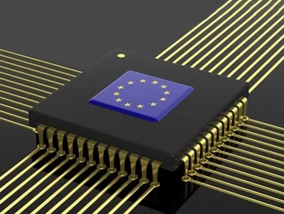
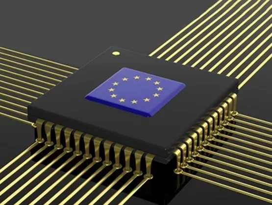
Last month, leading-edge equipment company ASML announced a surprising €1.3 billion investment into French AI company Mistral. The two companies touted stronger collaboration and the desire to “innovate faster together.” Even though some observers were skeptical, the commitment of one European tech champion into an aspiring European tech firm in the world’s hottest industry made plenty of sense. Writing for Bloomberg, columnist Lionel Laurent noted that such a deal was “a win for Europe’s tech ambitions” and that Mistral would have increased credibility in an AI race dominated by the United States and China.Europe’s tech prowess indeed lags behind its global rivals. ASML is, perhaps surprisingly (or not, depending on your vantage point), Europe’s largest tech giant by market cap at $406 billion. Europe boasts no tech goliaths the size of Amazon or NVIDIA and is often left following the lead of American tech firms as they chart the commercialization of new technologies. In the semiconductor industry, Europe’s chip manufacturers comprise only 9% of global market share today compared to 44% in 1990. Despite the bleak reality that Europe’s tech ecosystem finds itself in, there are reasons to believe that the nadir of recent years is slowly giving way to a more robust and respected innovation landscape. This piece will focus specifically on semiconductor manufacturing, demonstrating how Europe is taking its technological future seriously, and how, despite the challenges that remain, ultimately Europe is poised to succeed.Three Shocks – How We Arrived At This MomentThough Europe may not have been satisfied with the technological balance of power of recent decades, such an arrangement was largely tenable in a globalized world which prioritized free markets and international security in the aftermath of the Cold War. Though numerous cracks appeared in previous decades, the last five years in particular have given way to three shocks which have awoken European policymakers.The first, of course, was the COVID pandemic and the decimation of supply chains that caused a rapid seesaw in chip inventories – from extreme shortage to extreme oversupply – that companies in the automotive and industrial sector are just now recovering from. One senior German official was quoted as saying, “We lost 1-1.5% of our GDP in 2021 because of a lack of semiconductors – or about €40 billion.”Only two years later would come Russia’s unthinkable invasion of Ukraine, an unwelcome new reality which has forced Europe to reckon with its defense posture and supply chain. Semiconductors, again, play a key role here – Europe is reliant on China’s legacy chip production, meaning that low-tech chips often find their way into strategic weaponry.Lastly, a second Trump administration has surprised and rallied European governments to respond to “America first” rhetoric. Combined with the aforementioned shocks, recent events have convinced even Europe’s most ardent globalists that the continent must now invest where necessary in order to protect its borders and foster a competitive and sovereign technology ecosystem.The Underwhelming Response So FarFast forward to today where Europe’s COVID supply chain disruptions quickly gave way to ambitious policy in the form of the €43 billion European Chips Act intended to stimulate private investment to complement public capital and push Europe’s chip manufacturing market share to 20%. In the more than two years since the legislation’s passing, however, announced projects have underwhelmed. Big splashes from Intel and Wolfspeed have failed to materialize due to overambitious market expectations. Today, you can almost count the key recipients on one hand – STMicroelectronics, Infineon, TSMC, GlobalFoundries, Silicon Box, and amsOSRAM.Despite the sense of cynicism from some corners, however, understanding the slow progress to this point helps to unlock the right strategies moving forward. Already, many industry stakeholders and policymakers have questioned if attracting manufacturing full stop is the right strategy. Peter Wennink, former CEO of ASML, called the European Commission’s target to secure 20% of the global chip market by 2030 “totally unrealistic,” emphasizing that Europe’s current share is “8% at best.”Even if Wennink’s conclusion is too harsh, the tangible lack of investment over the past couple of years paired with the urgent need for Europe to maintain and grow its semiconductor prowess in response to concerns of security and sovereignty still demands a workable solution. The answer lies in building upon Europe’s very real strengths in the chip industry, narrowing the scope of investment to key strategic areas and in continuing to prioritize collaboration at all costs. How Europe Can Still Meet The MomentAny conversation about Europe’s contributions to the global semiconductor industry should begin with its unparalleled research ecosystem, and there’s no better place to start than with Belgium’s imec, one of the foremost research institutions chip companies depend on. Earlier this year, imec’s President and CEO Luc Van den hove emphatically reminded his audience that “you can’t make an advanced chip without European technology.” Van den hove’s point was that Europe should be leaning into its strengths as a research powerhouse rather than trying to chase leading-edge nodes. The FAMES Pilot Line is one example of what that research prowess looks like in practice. Funded with €830 million via the EU Chips Act, the initiative brings together Europe’s leading research institutions (imec, Fraunhofer, CEA-Leti, and Tyndall) to develop open access to several key microelectronic technologies, with a strong emphasis on low-power applications for markets such as automotive, IoT, and mobile devices. Central to FAMES is its “open access” policy which enables European manufacturers to use its pilot line to develop prototypes and evaluate next-generation technologies. Chip companies without any manufacturing presence in Europe stand on the outside looking in, risking technological inferiority.While Europe flexes its academic prowess, however, it is increasingly recognizing its vulnerability when it comes to more mature-node technologies and production. Investments such as ESMC – TSMC’s joint-venture with regional champions Bosch, Infineon, and NXP – are a good start, but Europe fundamentally needs more mature tech, particularly for defense. In a recent piece for Foreign Affairs Magazine, authors Chris Miller and John Allen argued that Europe indeed has a promising semiconductor opportunity ahead of it, but only if it enhances cooperation with the United States. The fact that the two regions have similar goals and geopolitical rivals is an opportunity for Europe to attract greater chip investment from U.S. firms looking for Europe’s leading research capabilities and defense customers. The authors implore European policymakers to:“ensure that their chip companies can capitalize on the surge in defense spending by investing more in new defense technologies and fostering connections between large chip firms and small defense start-ups. European chip companies that have previously focused on civilian markets must realize that the defense industry, and particularly the drone sector, will drive growth and technological change.”Targeting these investments intelligently remains to be seen, but there can be no doubt that Europe is taking the funding challenge seriously. Germany, France, Italy, and the United Kingdom have all raised their defense spending as a percentage of national income, with Germany announcing plans to double its defense spending to €650 billion over the next five years.Securing Position In Europe's Semiconductor RenaissanceEurope’s semiconductor future will not be built by mimicking Taiwan’s fabrication prowess or outspending America’s subsidies. Instead, success lies in doubling down on what Europe already does exceptionally well – world-class research infrastructure, strategic positioning in mature and specialty nodes, and an increasingly robust defense industrial base hungry for secure semiconductor supply. As European chip subsidies continue and defense budgets surge across the continent and geopolitical fractures deepen, the strategic calculus is clear – semiconductor companies without meaningful European capacity risk ceding ground to competitors who recognized the shift early. The question is no longer whether Europe matters in the global chip ecosystem, but rather which companies will position themselves to capitalize on its inevitable growth.About Stephen M. RothrockStephen Rothrock founded ATREG in 2000 to help the world’s advanced technology companies divest and acquire infrastructure-rich manufacturing assets, including wafer fabs (front- and back-end) as well as MEMS, solar, display, and R D facilities. Over the last 25 years, his firm has completed 40% of all global operational wafer fab sales in the semiconductor industry, a total of 60 transactions. Recent global acquisitions and dispositions have involved Allegro MicroSystems, Bosch, Elmos, Fujitsu, GlobalFoundries, IBM, Infineon, Japan Display (JDI), Micron, NXP, onsemi, Qualcomm, Renesas, Sony, Texas Instruments, and VIS to name just a few. Prior to founding ATREG, Rothrock established Colliers International’s Global Corporate Services initiative and headed the company’s U.S. division based in Seattle, WashBefore that, he worked as Director for Savills International real estate brokerage in London UK, establishing their global corporate services platform serving large multinationals, many of whom were leading technology companies. Rothrock also served on the UK-listed property company’s international board. He spent four years near Paris, France working for an international NGO. Rothrock holds an MA degree from the University of Hull, UK and a BA degree in Business Commerce from the University of Washington in Seattle, USA.
Read More
Political leaders worldwide are investing hundreds of billions to reduce semiconductor dependencies and secure their positions in this nearly $630 billion market, according to the World Semiconductor Trade Statistics (WSTS). Yet the extreme specialization and geographic concentration of the semiconductor supply chain makes complete self-sufficiency economically impractical and strategically questionable.After decades building an intricate global production network optimized for cost and innovation, the industry now faces pressure to splinter into regional blocks. But this raises important questions: Can any nation truly achieve chip self-sufficiency? And would disconnecting from the global ecosystem ultimately hurt competitiveness more than help security?The Independence IllusionThe global semiconductor industry has carved itself into specialized kingdoms. The United States dominates chip design and certain equipment categories, representing about 50% of global revenue. Taiwan controls roughly 67% of global foundry capacity through TSMC—so much so that semiconductors represent one-sixth of Taiwan's total GDP. Europe's strength lies in ASML's advanced EUV lithography technologies, the machines everyone needs but only one company currently makes.China plays an interesting double role too: it's both the largest semiconductor consumer at 50% of the global market and an important producer, holding 31% of total global foundry capacity in 2023.So far, every "independence" initiative has deepened interdependence. The US needs the Netherlands for lithography equipment. Europe needs Asia for high-end chip production. China develops much of its own equipment but remains dependent in key areas. The House of Cards ProblemFor decades, the semiconductor industry perfected making incredibly complex products cheaper every year through extreme specialization. Each company focused on one slice of the supply chain and became world-class at it. But nobody talked about what we built: a house of cards. The entire global economy now depends on a supply chain so specialized that losing even one supplier can shut down entire industries.The COVID pandemic exposed what industry insiders had warned about for years: the chip supply chain works brilliantly until it doesn't. When it fails, it fails spectacularly. The automotive industry alone lost $210 billion in 2021, and some manufacturers still haven't fully recovered.This 2021 chip shortage wasn't just a pandemic problem. Currently, rising geopolitical tensions are changing a supply crisis into a strategic nightmare, forcing countries to rethink their entire approach to semiconductors and their production.The Barriers to IndependenceThe semiconductor industry faces serious barriers that make true independence incredibly difficult for any single nation.First, the supply chain depends on chokepoints controlled by just a few companies in specific regions. Electronic Design Automation tools—essential software for designing any chip—come mostly from three US companies: Synopsys (~31%), Cadence Design Systems (~30%), and Siemens EDA (~13%). Without these design tools, you simply cannot create modern semiconductors. Manufacturing equipment presents an even tighter bottleneck, with ASML holding 100% control of EUV lithography machines needed for advanced chips. Second, the talent shortage makes building new capabilities nearly impossible. By 2030, semiconductor companies will need 1 million additional skilled workers. Developing semiconductor expertise takes a decade of hands-on experience, and most skilled professionals already work in established industry clusters like Taiwan, South Korea, and Silicon Valley. You can't simply relocate these engineers or train new ones quickly enough to staff multiple new regional semiconductor industries.Third and finally, resource requirements exceed what most countries can realistically provide. Building advanced semiconductor chip plants costs $20-30 billion each and they take years to construct before producing a single chip. These facilities consume up to 15 million litres of ultra-pure water daily and large facilities require up to 100 megawatt-hours of power per hour. Beyond the physical infrastructure, technical complexity has made first-time silicon success rates drop to just 14%, while 40% of semiconductor demand still comes from older process nodes, requiring completely separate supply chains for different chip generations.The Trillion-Dollar Investment RaceConcerns about supply chain security have triggered government interventions worldwide. The United States committed $52.7 billion through the CHIPS Act plus additional tax credits. While President Trump initially called for eliminating the program in March 2025, he instead signed an executive order on March 31, 2025, creating the "United States Investment Accelerator" to take over CHIPS Act implementation. TSMC also announced a new $100 billion investment to build five additional chip facilities in the US.Countries across the globe are racing to establish or strengthen their semiconductor capabilities. India has entered the semiconductor competition with its $10 billion Semiconductor Mission and secured investment from Micron Technology, which is constructing a $2.75 billion assembly and test facility. Japan has intensified its semiconductor strategy by establishing Rapidus Corporation with a government support package that is estimated to reach $11.46 billion aimed at revitalizing its domestic chip industry. Meanwhile, the European Union has established a €43 billion Chips Act through 2030, China launched its third "Big Fund" phase in May 2024 with $47.5 billion, and South Korea has developed a $450 billion K-Semiconductor strategy through 2030.These initiatives are changing the semiconductor industry on a global scale. However, complete self-sufficiency would require significant additional global investment and result in 35-65% semiconductor price increases due to suboptimal scale and inefficiencies.What Comes NextThe quest for chip self-sufficiency has become a trillion-dollar global endeavor, with countries placing enormous bets on facilities that may not pay off for years. Complete semiconductor independence remains financially prohibitive for any country, but strategic resilience is achievable.The winners will be those who build the most resilient networks and manage interdependence best. Rather than chasing impossible independence, nations should focus on strengthening their existing advantages while addressing their most vulnerable dependencies. Full independence remains a fantasy, but smart interdependence offers a realistic approach to semiconductor security.Click here to read the full white paper.About the AuthorsJan-Bart Smits is a Managing Partner at Stanton Chase Amsterdam. He began his career in executive search in 1990. At Stanton Chase, he has held several leadership roles, including Chair of the Board, Global Sector Leader for Technology, and Global Sector Leader for Professional Services. He currently serves as Stanton Chase’s Global Subsector Leader for the Semiconductor industry. He holds an M.Sc. in Astrophysics from Leiden University in the Netherlands. David Harap is a Managing Director at Stanton Chase Austin, bringing over 25 years of executive search experience to his role. He has successfully placed hundreds of senior executives and functional leaders across various industries. A Cornell University graduate and Father Kelly Scholar, Harap lectures at the University of Texas at Austin. He is a certified Ambassador for Hofstede Insights, bringing unique insights on organizational culture to his work.
Read More
Extended Plateau, Not a New Cycle: The Broader Industry PictureThe current recovery in the semiconductor market appears to signal revival, yet is best understood as an extended phase of the existing cycle—a phase defined less by renewed demand than by structural restraint and efficiency-driven realignment.AI-related demand is indeed driving the rebound, yet this recovery differs fundamentally from past expansionary booms. It is unfolding within an efficiency-driven adjustment phase, where capital expenditure has shifted its focus from capacity expansion to process upgrades and optimization. The observed recovery therefore reflects structural realignment rather than a conventional cyclical upswing.This realignment has created an ‘Extended Peak Plateau’—a state not of cyclical acceleration but of structural transformation. The imbalance between resilient equipment and materials spending and stagnant wafer shipments has produced an uneven recovery, concentrated in select high-value segments rather than evenly across the value chain. The apparent plateau seen today stems less from broad-based demand expansion than from price-anchored growth, sustained by firm pricing in premium segments such as AI-related and high bandwidth memory (HBM) products.At the same time, semiconductor manufacturers—particularly in memory—have adopted a supply-controlled operational strategy, emphasizing process optimization and product upgrades over large-scale capacity additions. Together, these three structural forces—supply/demand imbalance, price-anchored resilience, and efficiency-oriented adaptation—have defined the industry’s current phase, where revenue growth remains elevated but plateaued rather than accelerating or decelerating.In this context, the recent rise in DRAM prices and continued hyperscaler investment hold implications beyond short-term variables: They determine whether the industry can sustain equilibrium without widening the amplitude of future cycles between overheating and contraction. If DRAM recovery remains purely supply-driven, the upturn will likely be shallow; conversely, a slowdown in hyperscaler investment could undermine the demand foundation itself.This is why the report characterizes the current phase not as a “new cycle” but as an extended plateau. While AI-driven momentum has already taken hold, the transition toward a stable and balanced industry structure must pass through the filter of efficiency. This efficiency-based rebalancing will, in all likelihood, require a period of adjustment before a truly sustainable equilibrium — the foundation for the next phase of genuine growth — can emerge.Desynchronization Between Investment and Wafer Demand: Evidence of a Structural ShiftThe chart below visually illustrates this structural asymmetry. When normalized to Q1 2019 = 100, as of Q2 2025 equipment investment has rebounded to roughly 244, photoresist revenue to 200, and total semiconductor revenue to 184—yet wafer shipments remain near 110 and wafer revenue around 103.Diverging Trends Across the Semiconductor Value Chain (Q1 2019 = 100) * Note1. Data sources: SEMI (WWSEMS, Silicon Wafer Shipment, Photoresist Market Data), WSTS, and IR disclosures from the top five wafer suppliers.2. Wafer revenue reflects the aggregated sales of the top five suppliers; Shin-Etsu’s quarterly figures are estimated from 2Q 2021 onward.3. Semiconductor fab equipment investments reflect only wafer-processing equipment (WFE) expenditures, based on the Wafer Processing Equipment category defined in SEMI’s WWSEMS dataset. All indices are normalized to Q1 2019 = 100; wafer area shipments are originally reported in million square inches (MSI), while other indicators represent revenues or investments in U.S. dollars (USD). The data clearly indicate that while equipment and materials have rebounded, wafer shipments and related revenue remain subdued. This divergence is not a matter of cyclical timing; rather, it reflects a re-alignment of the industry’s recovery dynamics, driven by process complexity and efficiency-oriented capital deployment. In other words, the widening gap between investment and wafer industry output symbolizes the industry’s transition from expansion-driven growth to efficiency-driven operations.In previous cycles, the linear linkage of “investment expansion → production expansion” prevailed. Today, however, investment is now synonymous with process-efficiency improvement rather than capacity growth. Behind this shift lie longer cycle times, rising process complexity, and the increasing concentration of demand in AI-related nodes. More complex manufacturing now requires process sustainment, advanced process control, and continual upgrades—CapEx allocation now reflects this shift.At the same time, a clear gap has emerged between wafer revenue and shipment growth, underscoring the divergence between financial recovery and physical output. In other words, shipment volumes have improved, but average selling prices remain subdued, signaling that the recovery is not demand-driven. This indicates that the current phase is sustained not by broad-based demand expansion, but by selective growth achieved through efficiency gains and product-mix adjustments. Despite this widening gap, the industry may give the outward impression of a steady growth plateau, since CapEx spending and high-value segments continue to post solid growth. Yet what appears as stable growth in the semiconductor and equipment market could be, in fact, a structural illusion—a state shaped by process complexity, efficiency-driven investment, and deliberate product-mix management. In short, this perceived growth is the by-product of financial and supply discipline, not the result of renewed demand momentum.Realignment of the Wafer Industry: A Gradual 300 mm-Led Shift Anchored in Efficiency and Portfolio StrategyAs the broader semiconductor ecosystem shifts its focus from expansion to efficiency—and from scale to high value and customer reliability—wafer manufacturers are, in turn, redefining their competitive edge around operational efficiency and the stable delivery of high-value products. The 300 mm wafer segment continues to lead the recovery, whereas 200 mm wafer shipments remain significantly below its 2022 peak, constrained by sluggish demand from legacy and non-memory applications. On the profitability front, depreciation burdens and persistent pricing pressure are creating dual headwinds.To navigate this environment, leading wafer suppliers are pursuing a dual-track approach: renegotiating long-term supply agreements (LTAs) while managing short-term contracts and selective and disciplined pricing to sustain utilization. At the same time, they are optimizing product portfolios to balance cash-flow defense with strategic offense. In this context, the critical question is shifting from “How much can be sold?” to “What kind of portfolio—specifically, how consistently can high-value wafers be sold and delivered?”In essence, performance is now measured less by expansion and investment scale, and more by efficiency, sustainability, and reliability. This strategic realignment mirrors the broader efficiency-driven transition underway across the semiconductor value chain, underscoring that the wafer industry is no exception to the global shift toward disciplined, portfolio-centric growth.Conclusion: The Path to True Recovery — When Three Forces AlignIn summary, the current semiconductor market is best understood as having entered an extended plateau following the peak of the present cycle, with its future trajectory hinging on how effectively DRAM price resilience and Big Tech investment continuity can restore balance. In essence, the outcome will depend on the market’s ability to narrow the amplitude between overheating and contraction, moving toward a more sustainable equilibrium. Rather than focusing on the DRAM price rebound driven primarily by supply adjustments or on demand concentrated in specific sectors, what truly matters for the wafer industry is the structural alignment of three key forces: (1) the recovery of broad-based and genuine demand, (2) the stabilization of the semiconductor supply structure, and (3) the improvement of operational efficiency across the value chain. The moment these three forces align will signal the true onset of the next upcycle — not only for the broader semiconductor market, but also for the global silicon wafer industry.Such alignment rarely occurs quickly — it requires time, discipline, and structural patience.This article distills the key insights from the Market Update section of the Q3 2025 Silicon Wafer Market Monitor Report. In this quarter’s analysis, the focus lies on the semiconductor cycle’s transition into an Extended Peak Plateau — a phase characterized not by broad-based expansion, but by efficiency-driven operations and portfolio realignment. Drawing on shipment, revenue, and CapEx data across wafers, materials, and equipment, this section identifies structural asymmetries between investment and shipment dynamics, and explores how efficiency gains, product-mix optimization, and supply discipline are reshaping the industry’s recovery trajectory.Separate from this focused article, the full SEMI Silicon Wafer Market Monitor Report provides a wider array of charts and indicators, offering a multidimensional perspective on how key variables interact to shape the future of the global wafer industry. Rather than serving as background commentary, the full report aims to deliver data-driven, decision-ready insights that support strategic thinking amid persistent market uncertainty.For more information on the report or to subscribe, please contact the SEMI Market Intelligence Team at [email protected]. Details on SEMI market data are available at SEMI Market Data. Sungho Yoon is a Principal Analyst on the SEMI Market Intelligence team.
Read More
The SEMI Semiconductor Manufacturing Cybersecurity Consortium (SMCC) Work Group 3 (Supply Chain Cybersecurity) just released a major work product that will have a significant and lasting positive impact on the industry: the “Standardized Semiconductor Cyber Assessment (SSCA)” questionnaire. Creating a common security assessment process for device makers, equipment suppliers, software suppliers and other members of the global manufacturing value chain has been one of the principal focus areas for the SMCC from its outset. Its aim is to replace the plethora of company-specific questionnaires that are maintained, distributed, filled out, evaluated, and discussed. Given the breadth and importance of this objective, the work group involved expert stakeholders from across the globe, and the quality of their collective efforts reflects the robustness of this approach.This first-of-its-kind resource helps companies:Evaluate cyber readiness and reduce supply chain riskStreamline compliance with one standardized assessmentBuild trust and share results across multiple clientsAlign with NIST CSF 2.0 and industry best practicesHow is the SSCA structured?The questionnaire takes its basic structure from the Capability Maturity Model Integration (CMMI) framework, which is designed to improve and integrate processes across multiple disciplines, such as software development, system engineering, system testing, and even people management. It defines five distinct maturity levels for the relevant parts of an organization or aspects of a major topic (see figure below) with general explanations of what it means to be at a particular level.Source: WikipediaWorkgroup 3 tailored this model to the unique cybersecurity challenges faced by the semiconductor manufacturing supply chain, identifying six activity areas inspired by the NIST Cybersecurity Framework 2.0—Govern, Identify, Protect, Detect, Respond, and Recover. Within each area, there are specific descriptions of the attributes an organization must exhibit to be at a certain level.What does the SSCA include?The SSCA is delivered in multi-tab spreadsheet form with a tab of instructions and a tab of questions. Some of the questions are multiple choice (“Which CMMI maturity level are you, based on the attributes listed?”) and many are Yes/No (“Does the organization use secure technologies to share sensitive data with suppliers?”). In total, there are 165 questions across the six activity areas.The latter is already offered in five languages: English, Korean, Traditional and Simplified Chinese, and Japanese.How can I get the SSCA?Click here and fill out the form to download the SSCA.“Remembrance of Things Past” or has this ever been done before?No… and sort of.Those of you who remember the state of the semiconductor manufacturing industry in the early 90s will recall that one of the biggest problem areas was the poor and inconsistent quality of the embedded equipment control and communication interface software. SEMATECH and its member companies saw this as an ideal pre-competitive domain for the consortium’s focus, so the Manufacturing Systems Division evaluated best practices in the software engineering community of that era and selected the Capability Maturity Model (CMM) of Carnegie-Mellon’s Software Engineering Institute. Sound familiar?While wholly adopting the CMM at that time was beyond the reach of most equipment suppliers, the nugget that emerged was the decision to standardize on a set of “4-Up” charts that conveyed the most basic of software quality metrics. This got everyone using the same vocabulary, definitions, and visualization techniques to compare progress across process areas and timeframes, which was instrumental in identifying and addressing the root causes of the software issues. An example of a typical software quality “4-Up” chart appears below.Source: Techno-pmAnd in related news!Given the WG 1,2 recent (mid-July) release of the SEMI E187 Compliance Guidance document and the formation of the new South Korea Cybersecurity Work Group (WG9), the SMCC is poised to realize its vision of accelerating the adoption of SEMI Cybersecurity standards while creating vital complementary material.For more information or to participate in the cybersecurity working groups at SEMI SMCC, please contact Mayura Padmanabhan at [email protected] Weber is the VP, New Product Innovations at PDF Solutions and a long-time SEMI Standards participant, currently co-leader of the Equipment Data Publication Task Force and Computer and Device Security Task Force.
Read More
The semiconductor industry faces an unprecedented paradox: AI demand is booming, fab investments are rising, yet wafer shipments remain stubbornly flat. What's driving this disconnect, and when will it break?As of mid-2025, the global silicon wafer market appears calm on the surface, but underlying structural tensions are quietly mounting. The demand for AI semiconductors remains resilient, and certain high-value supply chains continue to operate near capacity. Yet wafer shipments have shown little sign of meaningful recovery—a divergence that raises questions about the conventional supply-demand playbook.SEMI's latest Silicon Wafer Market Monitor Report begins with a structural hypothesis: that the current market dynamics cannot be explained solely by weak demand or delayed orders. Instead, we propose that the demand pattern of fab operations itself has fundamentally changed.The Hidden Constraint: Time ExtensionOne critical metric has emerged as a structural bottleneck—fab cycle time, or the average duration for a wafer to complete its full process flow. Our quantitative analysis reveals that since 2020, fab cycle times have grown at a compound annual growth rate of 14.8%. This represents a fundamental deceleration in fab throughput, meaning that even with the same number of tools and consistent utilization rates, the volume of wafers that can be processed is now structurally constrained.Why is this happening? Rising process complexity, increased equipment density, and tighter quality control requirements are absorbing more capital per wafer while paradoxically slowing production. Equipment spending per wafer area has surged over 150% since 2020, yet this investment translates into longer processing times rather than higher throughput.The High Bandwidth Memory (HBM) Economic ThresholdSimultaneously, the market is approaching a new inflection point driven by the rapid rise of HBM. HBM wafers consume over three times more wafer area per bit compared to standard DRAM, creating potentially significant wafer demand. However, HBM currently accounts for just 16% of total memory revenue—still below a critical economic threshold.Our analysis identifies that when HBM reaches 25% of total memory revenue, the trade ratio rises to 1.5. This is the structural breakeven point where CapEx per wafer for HBM-dedicated lines aligns with standard DRAM economics. At this threshold, memory makers gain clear incentives to expand wafer input, and customers become more willing to pay premium prices.The Quantitative FrameworkInstead of relying on conventional forecasts, we model the interaction of four critical variables—HBM penetration, DRAM bit growth, fab utilization, and cycle time—using a quantitative simulation framework. Under current conditions (16% HBM revenue share, 15% annual bit growth, 95% fab utilization, and 14.8% cycle time increase), wafer input would need to increase by 23.9% annually to meet projected demand.Yet no fab is scaling wafer input to that extent today. This suggests the market isn't demand-constrained but operating within a conditionally responsive system—one that won't activate until key thresholds align.Beyond Economics: Technical and Operational ReadinessThe slow pace of HBM expansion isn't solely about investment timing. Technical constraints including low yields, delayed customer qualification, and process stabilization challenges also play critical roles. These preconditions—investment readiness, yield optimization, and qualification completion—haven't yet aligned, keeping the market in strategic latency despite robust underlying demand.Additional factors compound this delay. Backend bottlenecks in Chip-on-Wafer-on-Substrate (CoWoS) packaging are causing semi-finished wafers to accumulate as inventory, constraining upstream wafer input. At the fab level, companies prioritize efficiency gains through process conversions over new construction. Meanwhile, macroeconomic uncertainty, geopolitical tensions, and foreign exchange volatility continue suppressing capital execution.The Three-Tier Response ModelThis structural shift creates a three-tier demand response across the supply chain:Wafer demand: Conditionally responsive, awaiting economic threshold alignmentEquipment investment: Process-transition driven, already responding to complexity increasesMaterials demand: Directly tied to cycle time extensions, with potential for early bottlenecksFor certain process-critical materials like EUV photoresists and TSV chemicals, supply constraints may emerge even before wafer input fully ramps, preceding equipment expansion.Strategic ImplicationsFor industry stakeholders, this analysis suggests three key actions: wafer suppliers should prepare scenario-based capacity plans around the 25% HBM threshold; equipment makers should anticipate process-transition driven demand regardless of current wafer volumes; and materials suppliers should prepare for potential bottlenecks as extended cycle times increase consumption per wafer.Crucially, the current stagnation shouldn't be interpreted as structural decline. Rather, the market exists in a state of strategic readiness, with key conditions not yet aligned. Once they are, wafer demand will likely respond nonlinearly—and momentum is already building in that direction.The structural inflection point (≈25% HBM penetration) and cycle time increase (+14.8%) serve as forward-looking indicators not just for wafer producers, but for the entire upstream supply chain. The question isn't whether this inflection will occur, but when. Companies that understand these structural dynamics and prepare accordingly will be best positioned to capitalize on the nonlinear demand response when it arrives.These key insights are from the market update section of the Q2 2025 Silicon Wafer Market Monitor Report. This quarter's analysis models structural inflection points using scenario-based projections across nine core charts and tables, offering data-driven perspective on the industry's readiness for the next demand shift. Download your free sample report today.For more information on the report or to subscribe, please contact the SEMI Market Intelligence Team at [email protected]. Details on the complete SEMI market data portfolio are available at our Market Intelligence website. Sungho Yoon is a Principal Analyst in the Silicon Wafer Market Research at SEMI Market Intelligence.
Read More
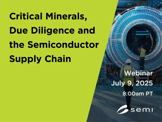
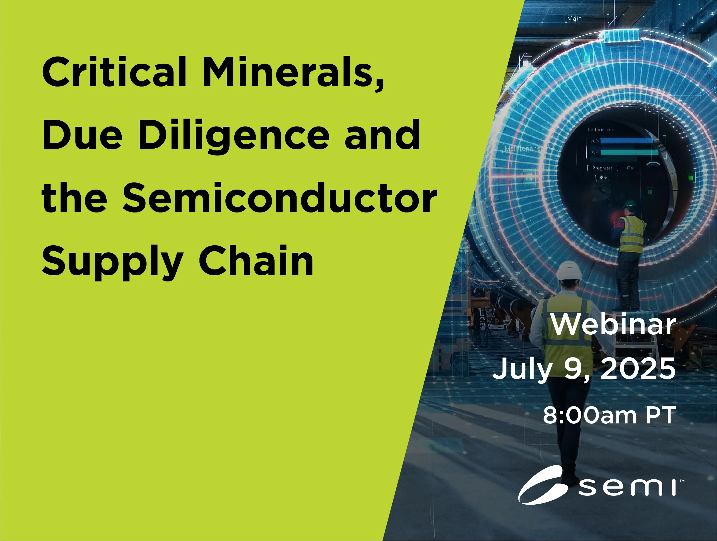
“Critical minerals our world needs for electric vehicles and semiconductors can be found here. Clean energy we need to power artificial intelligence data centers and economic growth can be built here.”[1] This statement was made by former US President Joseph Biden during his visit to Angola in December 2024 to support a US-funded railroad project called the Lobito Corridor. The railroad would connect mining areas in the Democratic Republic of Congo (DRC) and Zambia to a port on the western coast of Africa, an important step towards expanding access to critical minerals needed for growth of the semiconductor and energy industry in the west. According to the Intergovernmental Forum on Mining, Minerals, Metals and Sustainable Development (IGF), “there is no universally agreed upon definition of what ‘criticality’ means…criticality is also very country- and context-specific, particularly with respect to mineral endowment, the relative importance of the minerals to industrial and economic development, and a strategic assessment of supply risks and volatility.”[2] In other words, the term “critical mineral” may vary by location, application, and current events. Many countries have generated their own lists of critical minerals to help guide legislation, budgetary allocations and diplomatic efforts. For example, the United States Geological Survey released a list of “50 mineral commodities critical to the US economy and national security” in 2022 which included 10 minerals that were directly linked to semiconductors and electronics.[3] These included arsenic, dysprosium, gallium, lutetium, rhodium, ruthenium, tantalum, terbium, tin, and tungsten. Other lists might include cobalt, copper, and sometimes uranium. For most countries that make chips and electronics, critical minerals are both essential for supporting their industry and also hard to find within their own borders.While downstream electronics and semiconductor manufacturers are often located in countries with robust labor protections, the extraction of raw minerals too often takes place under less humane circumstances. In April 2024, the UN Secretary General launched the Panel on Critical Energy Transition Minerals to address the challenges associated with responsible extraction of critical minerals. One of the motivations for the formation of the panel was the concern about human rights violations related to mineral extraction. “Mining, at all scales, large and small, has too often been linked with human rights abuses, environmental degradation and conflict.”[4] The term “conflict mineral” has a much narrower definition than critical mineral, and usually only refers to tin, tantalum, tungsten and gold, also known as ‘3TG’. This definition is often used in policy frameworks, such as the US Dodd-Frank 1502 Act[5] and the European Union (EU) Regulation 2017/821[6]. These four minerals were identified as a major source of income for armed groups in the DRC, fueling a decades long war that has claimed more than 6 million lives since the start of the Second Congo War in 1996.[7] For example, in May 2024, armed groups from Rwanda captured a town in the Congo with the largest coltan mine in the country, which is the second largest producer in the world of the ore that is refined to make tantalum - a key component of capacitors. The incursion helped to finance the armed group, collecting at least $800,000 per month in taxes.[8] Over the past 15 years, several frameworks have emerged to address the conflicts and tensions stemming from extraction of critical minerals. A common framework within the semiconductor industry was written by the Organization for Cooperation and Development (OECD), which is an intergovernmental economic organization founded in 1948 (then known as OEEC) to “build better policies for better lives.” The organization publishes several guidelines, including the OECD Due Diligence Guidance for Responsible Business Conduct[9] (see suggested measures in Figure 1) and the OECD Due Diligence Guidance for Responsible Supply Chains of Minerals from Conflict-Affected and High-Risk Areas with focuses specifically on 3TG minerals.[10] These guidelines provide a structure through which companies and organizations might address human rights and environmental issues that may arise from their or their suppliers’ operations. Figure 1: Due Diligence Process and Supporting Measures from the OECD Due Diligence Guidance for Responsible Business Conduct (2018)Several regulations have been implemented by governing bodies to prevent financing of armed groups through procurement of conflict minerals. In the United States, Section 1502 of the Dodd-Frank Wall Street Reform and Consumer Protection Act requires certain companies to “publicly disclose their use of conflict minerals that originated in the Democratic Republic of the Congo or an adjoining country.”[11] Also known as the “Disclosure Rule,” a company must file a report to the Securities and Exchange Commission (SEC) describing the source and chain of custody of its conflict minerals, and must also conform to a nationally or internationally recognized due diligence standard such as the OECD guidelines. Similarly, the EU Regulation 2017/821 refers to the OECD Due Diligence Guidelines and calls on companies within the EU to monitor, audit and disclose procurement of conflict minerals. In 2024, the EU furthered its efforts to address human rights and environmental issues by adopting the EU Corporate Sustainability Due Diligence Directive (EU CSDDD). This directive will require all companies that do business within the EU, regardless of country of origin, to monitor their supply chains for labor and environmental violations or risk penalty.Given the tremendous effort by the industry to address the conflict associated with 3TG minerals, it is unclear whether these efforts have had an effect. The U.S. Government Accountability Office (GAO), which serves as the federal government’s watchdog agency and is tasked with providing Congress with independent, nonpartisan information, has been reporting on issues related to conflict minerals in the DRC since 2010. Kimberly Gianopoulos, Managing Director of GAO’s International Affairs and Trade Team, has led this body of work over time, including GAO’s most recent report, which was published in October 2024. Gianopoulos stated that, “although it has been over a decade since the SEC issued its conflict minerals disclosure rule in 2012, GAO’s most recent report found that there is no empirical evidence that the rule has decreased violence in the eastern DRC, where many mines and armed groups are located, and that a majority of companies that conduct due diligence on their mineral supply chains continue to report being unable to determine the origins of minerals used in their products.” The 2024 Conflict Minerals report can be found here: https://www.gao.gov/products/gao-25-107018.Regulatory approaches are only one way in which the semiconductor industry interacts with conflict mineral issues. Many companies and industry associations have implemented their own initiatives and formed associations to share resources to trace materials and collect supplier information. One such industry association is the Responsible Business Alliance’s Responsible Minerals Initiative (RMI). Jennifer Peyser, the executive director of the RMI, stated that the initiative “supports over 500 downstream, midstream, and upstream member companies with a suite of due diligence standards and tools, data, guidance, training, and other resources for global responsible sourcing and regulatory compliance. Our facility and supply chain due diligence standards are rooted in longstanding international norms while reflecting emerging corporate and stakeholder priorities for regulatory compliance, managing sustainability risks and impacts, and fostering responsible mineral supply chains.” More information about the RMI can be found here: www.responsiblemineralsinitiative.org.Recently, SEMI has formed a new Responsible Supply Chain (RSC) working group under its Supply Chain Management initiative to provide a platform for enabling traceability and provenance across the supply chain to meet government regulations on conflict minerals and unfair labor practices. This new working group aims to bring together SEMI member companies to raise awareness of key issues, share resources, and advocate effective regulations and standards. The working group is comprised of SEMI member company employees from a wide range of backgrounds, including sustainability managers, supply chain experts and process engineers. If you are interested in joining our discussions, please visit our website for more information: https://www.semi.org/en/industry-groups/supply-chain-management. On July 9 at 8am Pacific/11am Eastern, the SEMI Responsible Supply Chain working group will host a webinar featuring a roundtable discussion with Jennifer Peyser, Executive Director of the Responsible Business Alliance’s Responsible Minerals Initiative, and Kimberly Gianopoulos, Managing Director of the International Affairs and Trade Team at the US Government Accountability Office, including Q A for attendees to join the discussion. Visit https://www.semi.org/en/event/critical-minerals-due-diligence-and-semiconductor-supply-chain to register.Other upcoming events include a panel discussion at SEMICON West, October 7-9, 2025 in Phoenix, Arizona!Author Bio:Dr. Kimberly Harrison Ph.D is a Senior MEMS Designer with AMFitzgerald Associates, a design firm located in the Bay Area California. She has a doctoral degree in mechanical engineering from Stanford University, and has worked as a designer and process engineer in the semiconductor industry for 10 years. She was nominated as a 2022 MEMS Sensors Industry Group Emerging Leader. As a founding member and leader of the SEMI Responsible Supply Chain Working Group, she hopes to bring SEMI members together to discuss solutions to human rights issues in the semiconductor supply chain.References:[1] Remarks by President Biden Participating in the Lobito Corridor Trans-Africa Summit in Benguela, Angola (December 4, 2024). https://bidenwhitehouse.archives.gov/briefing-room/speeches-remarks/2024/12/04/remarks-by-president-biden-participating-in-the-lobito-corridor-trans-africa-summit-benguela-angola/[2] Critical Minerals: A Primer (November 1, 2022). https://www.igfmining.org/resource/critical-minerals-primer/[3] https://www.usgs.gov/news/national-news-release/us-geological-survey-releases-2022-list-critical-minerals[4] Resourcing the Energy Transition: Principles to Guide Critical Energy Transition Minerals Towards Equity and Justice (April 11, 2024). https://www.un.org/en/climatechange/critical-minerals[5] https://www.sec.gov/resources-small-businesses/small-business-compliance-guides/conflict-minerals-disclosure[6] https://eur-lex.europa.eu/eli/reg/2017/821/oj/eng[7] Conflict in the Democratic Republic of Congo (March 20, 2025). https://www.cfr.org/global-conflict-tracker/conflict/violence-democratic-republic-congo[8] The Evidence that Shows Rwanda is Backing Rebels in DR Congo (January 29, 2025) https://www.bbc.com/news/articles/ckgyzl1mlkvo[9] OECD Due Diligence Guidance for Responsible Business Conduct (February 1, 2018). https://www.oecd.org/en/publications/oecd-due-diligence-guidance-for-responsible-business-conduct_15f5f4b3-en.html[10] OECD Due Diligence Guidance for Responsible Supply Chains of Minerals from Conflict-Affected and High-Risk Areas, 3rd edition (April 6, 2016). https://www.oecd.org/en/publications/oecd-due-diligence-guidance-for-responsible-supply-chains-of-minerals-from-conflict-affected-and-high-risk-areas_9789264252479-en.html[11] https://www.sec.gov/resources-small-businesses/small-business-compliance-guides/conflict-minerals-disclosure
Read More
The semiconductor industry has long followed a well-defined cyclical structure. Typically, price declines lead to a contraction in capital expenditure, followed by inventory normalization and eventual recovery. This repeated pattern—comprising pricing correction, investment pullback, inventory adjustment, and eventual market rebound—continues to offer a relevant lens through which to interpret the current uncertain market environment.As of April 2025, the industry faces a mix of conflicting signals. Concerns are rising that AI-related demand may have already peaked, while cautious optimism persists over a possible rebound in DRAM prices in the second half of the year. These market dynamics are further complicated by rising macroeconomic uncertainty, including renewed trade friction between the U.S. and China, reemerging tariff risks, and persistent inflationary pressure. In such a complex and volatile environment, the importance of cycle-based structural analysis has never been greater.Viewed from a momentum perspective, the recovery in semiconductor equipment investment—marked by a rebound in year-over-year growth (measured on a 12-month moving average basis) beginning in mid-2024—can be interpreted as a potential sign of renewed demand. However, this apparent stability may be misleading. While global companies significantly curtailed their fab investments throughout the second half of 2023 and the first half of 2024, China moved in the opposite direction, intensifying state-led expansion efforts aimed at achieving semiconductor self-sufficiency. This divergence in investment behavior has distorted the global capital expenditure landscape, potentially creating the impression of a broader recovery, while in reality the momentum remains concentrated in a single region driven by policy rather than market fundamentals.Similarly, the recent uptick in DRAM pricing appears to be driven more by production cuts than demand-side momentum. Major suppliers have been deliberately scaling back output to manage inventory and support pricing. In this context, price rebounds not backed by end-market demand are unlikely to sustain a meaningful recovery in wafer procurement. Simulation results—based on second-half projections—suggest that unless DRAM blended ASP increases by more than 20% quarter-over-quarter in both Q3 and Q4 2025, a meaningful upward inflection in the year-over-year pricing trend (on a 12-month moving average basis) remains improbable. This highlights the fragility of the current price recovery suggests that without a meaningful improvement in end-market demand—particularly for DRAM—wafer procurement for DRAM production is unlikely to recover in a sustained manner, regardless of supply-side actions. As SEMI highlights in this Silicon Wafer Market Monitor Report, a deeper understanding of the wafer market requires a close examination of raw material inventory trends. The inventory behavior of memory makers—due to their dominant scale and transparency—is widely regarded as a proxy for broader semiconductor industry trends. Following the pandemic, memory makers' raw material stockpiles surged to levels equivalent to five times their historical average relative to sales. While these ratios were significantly reduced between 2023 and 2024, inventory levels still meaningfully exceed pre-pandemic norms. With leading players signaling further inventory drawdowns, there is little incentive to rebuild raw material stockpiles—including silicon wafers—unless there is clear evidence of sustained demand recovery.This inventory dynamic is closely tied to wafer shipment growth. Historical data reveals a strong inverse relationship between raw material inventory-to-sales ratios at the top three memory makers—Samsung, SK hynix, and Micron—and wafer shipments. When this ratio declines year-over-year, wafer shipment growth typically improves. However, a slowdown in the pace of inventory ratio reduction could result in stagnant or declining wafer shipment growth in subsequent periods.Moreover, even as these inventory ratios continue to decline, wafer average selling prices (ASPs) have yet to show signs of recovery. This decoupling of pricing from inventory adjustments reflects the presence of a structural imbalance in supply and demand. On the supply side, all top five global wafer producers have secured greenfield fab capacity and are prepared to scale production. With depreciation pressures mounting, they face strong incentives to maintain economically viable utilization rates, contributing to ongoing ASP erosion.Meanwhile, chip capacity expansion in China—primarily driven by demand for 200mm applications—is adding further downward pressure. Chinese wafer suppliers, who already hold a meaningful share in China’s 200mm market, are now directing more of their investment toward 300mm wafer production—intensifying price pressure and adding to the longer-term competitive pressures facing global suppliers. This focus aligns with China’s broader push into mature process nodes, even as demand outside the region remains tepid. Accordingly, local Chinese wafer suppliers are competing aggressively on price, weakening the regional competitiveness of established global wafer players.As a result, the competitive landscape is undergoing a structural shift: global wafer suppliers are contending with intensified price-based competition among themselves in non-China markets, while simultaneously coming under mounting pressure from Chinese local players within China. This dual-front competition highlights the threshold point the industry has reached—where traditional pricing models and market dynamics are being fundamentally challenged.Moreover, long-term supply agreements (LTAs), once effective tools for pricing stability, are expected to gradually lose relevance. As semiconductor manufacturers—who purchase wafers under LTAs—move toward shorter-term and more customized purchasing models, and as pricing volatility increases, the incentive to commit to such agreements is projected to steadily diminish. The market, therefore, is not yet in a phase of strong recovery but appears to be undergoing a structural transition defined by persistent imbalances. The full report presents three scenario-based outlooks centered on four key variables—DRAM pricing, inventory normalization, equipment investment, and China’s regional influence. The most probable scenario currently assumes modest growth in 2025–2026, a correction in 2027, and a recovery in 2028. Wafer shipment growth rates under this scenario are projected at +5.1%, +5.4%, –6.2%, and +9.8%, respectively.However, even this base case remains vulnerable to potential macroeconomic disruptions. The large-scale tariff measures announced by the U.S. in April 2025 could trigger cascading effects across the ecosystem—from weakening enterprise demand and delaying infrastructure investments to softening DRAM prices and curbing wafer procurement. In past cycles, leading macro indicators such as the OECD Composite Leading Indicators (CLI) tended to lead DRAM price movements. If macro momentum slows, the market could deviate from the base case and move closer to the downside scenario. This downside scenario assumes weak or negative growth through 2026, a moderate recovery in 2027, and a stronger rebound by 2028 as supply-demand conditions begin to normalize.The current market trajectory suggests limited room for either sharp declines or sharp rebounds. The next phase will depend on how four forces interact: DRAM price momentum, inventory rebalancing pace, regional investment activity, and policy risks. A clear inflection point will only emerge when these factors begin to align. In other words, a meaningful shift—either upward or downward—will only occur when these forces move in the same direction and reinforce one another. Ultimately, any directional shift—whether delayed or accelerated—will still unfold within the broader framework of the semiconductor cycle previously discussed. In that sense, these indicators do not reverse the cycle itself; they merely influence the timing and pace at which it plays out.This article presents a summary of key insights from the Q1 2025 Market Update section of the SEMI’s Silicon Wafer Market Monitor Report, which is compiled in PowerPoint format and distributed as a PDF. In this edition, scenario-based analysis was used to navigate growing macroeconomic uncertainty and assess potential turning points in wafer demand. To support this analysis, the Market Update section presents 10 core quantitative charts and long-term data series dating back to 2000—particularly curated to visualize and analyze semiconductor revenue, investment, and pricing cycles in a single view. Separate from this focused section, the full SEMI’s Silicon Wafer Market Monitor Report includes a much broader array of charts and indicators, providing a multi-dimensional analysis of how fundamental variables interact to shape the future of the silicon wafer industry. Rather than simply offering background explanation, the full report is intended to provide clear, data-driven insights that can support strategic thinking amid market uncertainty.For more information on the report or to subscribe, please contact the SEMI Market Intelligence Team at [email protected]. Details on SEMI market data are available at SEMI Market Data. Sungho Yoon is a Principal Analyst on the SEMI Market Intelligence team.
Read More
Geopolitical shifts, rapid technological advancement, and supply chain pressures continue to redefine the global semiconductor landscape. These forces framed the discussions at the 2025 SEMI Industry Strategy Symposium Europe (ISS Europe), held in Sopot, Poland. Over two days, industry leaders, and policymakers examined how Europe can boost resilience amid growing uncertainty.Artificial intelligence (AI) stood out as a key driver—powering global chip demand and transforming industry operations. In the past year, AI applications like generative models and edge computing helped push chip sales to new highs. The EU Chips Act, effective since September 2023, also fueled change. It has drawn tens of billions of euros into European semiconductor infrastructure, including major investments in Pomerania, the host region for this year’s symposium. “With AI expected to drive exponential growth in the semiconductor industry—projected to reach $1 trillion by 2030—Europe must act collectively to remain competitive,” said Laith Altimime, President of SEMI Europe. “We encourage collaboration across all countries to strengthen supply chain resilience, mitigate geopolitical risks, and harness the full potential of our diverse talent base.”Laith Altimime, President, SEMI EuropeSo what has the EU’s investment in the semiconductor industry achieved, and how much more remains to be done? Gustav Kalbe, Acting Director of Enabling and Emerging Technologies at the European Commission, cited €80 billion in public and private investment in European fabs as clear progress toward introducing "advanced technology that has not before been deployed on the continent of Europe." However, Kalbe emphasized a new urgency driven by AI’s rise. “We need in Europe a secure supply chain for AI chips in key sectors—particularly automotive,” said Kalbe. “That’s why we are really pushing for accelerated development of AI chips here.”Gustav Kalbe, Acting Director of Enabling and emerging technologies,DG CNECT, European CommissionPoland is a prime example of the EU Chips Act’s impact—driven by consistent government support. Dariusz Standerski, Secretary of State in the Ministry of Digital Affairs, highlighted Poland’s seven-pillar national semiconductor strategy, which includes expanding infrastructure and increasing engineering talent by 20% by 2030. “We need to build our production capacity to meet the strategic needs of Poland,” said Standerski. “Semiconductors are important not only because of market size, but because of their role in national security.”Dariusz Standerski, Secretary of State, Ministry of Digital Affairs, PolandRisks to the Industry from a World in Political TurmoilGeopolitical shifts and market volatility dominated the opening session of ISS Europe 2025. Malcolm Penn, CEO of Future Horizons, warned that despite strong 2024 revenues, industry fundamentals remain fragile. “All of the growth is in graphics processing units (GPUs) for AI and high-bandwidth memory (HBM) for AI servers—every other product sector is currently in recession,” said Penn. He forecast 12% industry growth in 2025 but cautioned against overcapacity and price pressures from China. “We are not seeing unit growth, and without unit growth, you don’t have sustainable market growth,” explained Penn. “If momentum in AI slows, the industry could face a significant retrenchment.”Malcolm Penn, CEO of Future HorizonsLooking beyond the immediate outlook for semiconductors, Hendrik Bourgeois, Vice President for European Governmental Affairs at Intel, turned the spotlight onbroader economic and security challenges facing the region. Bourgeois outlined four strategic policy priorities for Europe: Build internal strength to ensure external (global) relevance;Deepen alliances beyond the United States—such as with the UK, Canada, Japan, and South Korea;Be open to a stronger economic relationship with China;Recognize that the U.S. is more than its federal government: states, cities, people and corporations all have a role to play in bringing stability and certainty.Hendrik Bourgeois, Vice President for European Governmental Affairs, IntelBenedikt Ernst, Senior Vice President and Head of Strategy Transformation at Merck KGaA, Darmstadt, Germany, emphasized the strategic importance of strengthening Europe’s domestic semiconductor ecosystem. “No country or region can be fully self-sufficient,” said Ernst. “But Europe is particularly strong in domains like advanced materials, fabrication equipment, and semiconductor manufacturing. We have leading players in these fields – let’s bet on them.”Benedikt Ernst, Senior Vice President and Head of Strategy Transformation, Merck KGaA, Darmstadt, GermanyMikolaj Trunin, Deputy Director of the Invest in Pomerania, and its Strategic Investment Manager Radoslaw Bojarczuk, highlighted the region’s rising profile among global investors. Despite a global downturn in foreign direct investment (FDI) since 2015, the region stretching from Gdansk and Warsaw to Dresden and Magdeburg is emerging as a vibrant semiconductor hub. “The environment is becoming increasingly attractive to outside investors drawn by the region’s large talent pool, robust venture capital activity, and strong and stable economic growth,” said Trunin.Left: Mikołaj Trunin, Deputy Director, Invest in PomeraniaRight: Radosław Bojarczuk, Strategic Investment Manager, Invest in PomeraniaAdvancing on the Roadmap to Net ZeroThe symposium’s second session tackled sustainability—how to grow the industry beyond $1 trillion in revenue while cutting emissions. AI emerged as a key enabler of sustainable innovation. Bill Lussier, Managing Director of Tokyo Electron Europe, highlighted recycled aluminum which has a much lower carbon footprint, but noted that semiconductor equipment requires ultra-pure aluminum, which is not available off-the-shelf in recycled form. “The solution is to create a new circular economy for ultra-pure aluminum—a supply chain so complex that it cannot be managed without the aid of AI,” explained Lussier.Bill Lussier, Managing Director, Tokyo Electron EuropeAI is also helping decarbonize logistics, a critical yet often overlooked part of the semiconductor ecosystem. Rainer Kiefer, Executive Vice President and Global Head of Sales at Schenker AG, underscored the environmental cost of air cargo: “We need smart supply chain design to reduce the air miles of chips.” AI supports this by optimizing routing, loads, predictive maintenance, and demand forecasting. Rainer Kiefer, Executive Vice President and Global Head of Sales, Schenker AGHowever, AI brings new energy demands. Malgorzata Kasperska, Vice President of Secure Power at Schneider Electric, urged greater efficiency in AI data centers: “We need to optimize both power capacity and efficiency, and deploy high-density infrastructure, all while enhancing sustainability practices.” Malgorzata Kasperska, Vice President of Secure Power, Schneider ElectricEnergy-intensive fab operations remain a major challenge. Charles Vaillant, Chief Technology Officer at MANN+HUMMEL, noted that heating and ventilation account for up to 50% of a fab’s energy use. To improve efficiency, the company introduced a filtration system using activated carbon ceramic technology. The innovation reduces pressure drop, cutting fan energy use and delivering up to 41% energy savings in cleanroom environments.Charles Vaillant, Chief Technology Officer at MANN+HUMMELFinding the Talent to Fuel the Industry’s GrowthAttracting and developing talent remains a critical challenge for the semiconductor industry. Andreas Schleicher, Director for Education and Skills at the OECD, cited a visibility gap: “Young people don’t see these engineering and IT jobs. You cannot be what you do not see.” Meike Boekelmann, Chief Human Resources Officer at Comet, echoed the sentiment. “Face-to-face, we can get people excited about joining our industry,” said Boekelmann. “The challenge is getting them in front of us in the first place.” Andreas Schleicher, Director for Education and Skills,Organization for Economic Co-operation and Development (OECD)In a panel discussion on Bridging the Talent Gap for Sustainable Growth, moderated by SEMI Europe’s Maria Daniela Perez, speakers explored how industry and academia can better collaborate to meet evolving workforce demands. Thomas Kralinski, Saxon State Secretary of Economic Affairs, Labor, Energy and Climate, emphasized the importance of future-ready education. “Do we know which fab is going to be built in 2035, or which start-up will be founded? No—but all the people who will work there are already alive. We need education to prepare these people for this unknown future.Thomas Kralinski, Saxon State Secretary of Economic Affairs, Labor, Energy and ClimatePanel Discussion on Bridging the Talent Gap for Sustainable GrowthAI Intensifies Scale of Innovation in Semiconductor FabricationDay two of ISS Europe 2025 spotlighted AI’s transformative impact on semiconductor innovation, from materials to manufacturing and chip design. John Behnke, General Manager for Smart Manufacturing at INFICON, emphasized AI’s growing role in managing fab complexity. “You need a lot of highly knowledgeable people to run a fab today,” said Behnke. “They must analyze huge amounts of data, and balance priorities like quality, on-time delivery, cycle time, and profitability.” In the future, he explained, AI-powered optimization engines will shoulder that burden by making autonomous decisions.John Behnke, General Manager for Smart Manufacturing, INFICONJean-Christophe Eloy, CEO of Yole Group, pointed to the rapid growth of data centers as a catalyst for architectural transformation, predicting a shift from monolithic AI ASICs to chiplet-based designs. “In the future, we can expect to see much of the value in the semiconductor business transfer from the front-end chip to the advanced packaging that integrates chiplets,” said Eloy. Jean-Christophe Eloy, CEO, Yole GroupThis sentiment was echoed by Christophe Frey, Vice President of EU Engagement at Arm, who described the industry’s shift from systems-on-chip to systems-of-chips. “Chiplets represents a unique opportunity for Europe to re-enter the game of high-end chips,” said Frey. He emphasized the need for an open chiplet marketplace, an effort Arm supports, but warned, “There is a long road ahead of us,” citing the need for silicon qualification, profiling, test and debug infrastructure, software standards, and specifications for mechanical and thermal integration.Christophe Frey, Vice President of EU Engagement, ArmThat transition is already taking shape in manufacturing. Volker Herbig, Vice President of the Microsystems Business Unit at X-FAB, noted that capabilities developed for CMOS+MEMS sensor in the early 2000s are now enabling heterogeneous integration (HI) at scale. “We are now an open HI foundry,” said Herbig, adding that X-FAB is building a dedicated HI facility with support from the EU Chips Act. “This technology is propagating down from the high-performance computing (HPC) world to medical and industrial applications — It’s happening as we speak.”An Industry Changing Faster Than Ever Volker Herbig captured the industry’s rapid evolution with the “Red Queen” theory from Alice in Wonderland: “You need to run as fast as you can just to stay in the same place.”Volker Herbig, Vice-President, BU MEMS, X-FABClosing the symposium, Leonard Hobbs, Director for Government Affairs at Intel Ireland, cited Charles Darwin: “The species which can best adapt to changes in its environment is the one which survives,” Hobbs added, “Over the past two days we have learned much that can help Europe’s semiconductor industry to adapt successfully to a rapidly changed world.” Leonard Hobbs, Director for Government Affairs, Intel IrelandAt the symposium’s gala dinner, delegates celebrated leaders driving the industry forward. SEMI presented the 2024 SEMI European Award to Kurt Sievers, President and CEO of NXP Semiconductors, and honored Anna-Riikka Vuorikari-Antikainen, Chief Commercial Officer of Okmetic, with the Special Service Award.Kurt Sievers, President and CEO, NXP Semiconductors (Middle)Anna-Riikka Vuorikari-Antikainen, Chief Commercial Officer, OkmeticOn behalf of SEMI, the SEMI Europe team and ISS Europe committee would like to thank all speakers, sponsors, and attendees for making the event a great success.SEMI Contact Cassandra Melvin, Senior Director of Business Development and Operations Email: [email protected]
Read More
The European semiconductor ecosystem continues to evolve, driven by the ambitions outlined in the EU Chips Act. With goals to strengthen Europe’s technological leadership and double its semiconductor manufacturing market share to 20% by 2030, collaboration across the value chain is imperative. Heterogeneous Integration for Connectivity and Sustainability (HiCONNECTS), a Horizon Europe-funded project, exemplifies this collaborative spirit. The initiative aims to develop next-generation electronic components and systems using advanced heterogeneous integration core technology solutions.The HiCONNECTS consortium, comprising 65 partners with diverse expertise, is addressing key societal and industrial challenges. These efforts focus on advancing core technology solutions for energy-efficient, high-performance wireless and wired cloud and edge computing, as well as automotive radar systems.“Collaborating with 65 partners is no small feat—it’s akin to orchestrating a complex IT network,” says Ilan Englard, Coordinator of the HiCONNECTS project. “We streamline progress by creating local networks of partners, all interconnected through a central management framework of tasks, work packages, and coordination. Such large consortia form intricate systems where complexity fosters innovation, often leading to surprising and transformative outcomes.” As the three-year project progresses, HiCONNECTS is working to establish pilot lines focused on key areas:RF Electronic Heterogeneous IntegrationPhotonic Components for Heterogeneous IntegrationAdvanced Packaging for Heterogeneous IntegrationThese pilot lines, led by organizations such as the Ferdinand Braun Institute and imec, will develop systems and modules through advanced equipment development, manufacturing optimization, and integration of electronic and photonic components. Validation of equipment in integrated process flows will further enhance the heterogeneous integration landscape.Now in its third year, HiCONNECTS continues to welcome new members. This inclusiveness underscores the project’s flexibility and its commitment to incorporating fresh perspectives as new trends and challenges emerge. At the 12-month consortium meeting in Catania last February, Arbonaut was unanimously inducted to contribute to the forest fire use case, further expanding the project’s scope.“The upcoming months are critical, as we move closer to delivering modules, systems, and demonstrators,” says Englard. “Our goal is to heterogeneously integrate the next generation of RF, electronic, and photonic components into networking, telecom, and radar systems, with support from module and equipment makers.”HiCONNECTS members at the 12-month consortium meeting in Catania, February 2024As this ambitious work progresses, sharing project results and achievements remains a top priority for the consortium to ensure meaningful social, political, and economic impact. By drawing attention to the results of the project, the consortium enhances the visibility, comprehension, and implementation of these advancements. Recently, four partners—Excillum, TNO, SANLAB, and Centria University of Applied Sciences—participated in a webinar titled “Heterogeneous Integration for Future High Speed Communication,” organized by SEMI Europe. The webinar is now available on demand for viewers worldwide.The significance of HiCONNECTS was further highlighted at SEMICON Europa 2024, where seven consortium members presented progress on topics ranging from advanced packaging to photonic integration. At the TechARENA, representatives from SEMI Europe, Excillum, Centria, Arbonaut, AT S, imec, and Applied Materials showcased the project’s contributions to the semiconductor ecosystem. “I was thrilled to present at the TECHArena and engage with the HiConnects partners,” said Julius Hållstedt, Head of segment - Semi Electronics, Excillum. “I especially appreciated the high attendance at my talk, which validated the strong interest in X-ray solutions for semiconductor applications. The insightful discussions at the SEMICON Europa exhibition and advanced packaging conference was a rewarding bonus.”HiCONNECTS Speakers at SEMICON Europa 2024By disseminating research and breakthroughs across various channels, such as publications, webinars, and conferences, HiCONNECTS is promoting knowledge sharing and fostering collaboration across the semiconductor ecosystem. This openness accelerates the adoption of new technologies, ensuring that European industry players remain at the forefront of critical advancements. Furthermore, sharing these results strengthens Europe’s position as a hub for cutting-edge research and development, driving both economic growth and technological leadership on the global stage.SEMI Europe is proud to be a consortium member of HiCONNECTS under the Chips Joint Undertaking (Chips JU), which is funded by the EU Horizon Europe program and supported by numerous countries, including Austria, Italy, Germany, and Sweden.About HiCONNECTS:HiCONNECTS (Heterogeneous Integration for Connectivity and Sustainability) is a three-year project bringing together 65 partners to develop sustainable, energy-efficient cloud and edge computing platforms. The project focuses on high-performance computing, storage infrastructure, network interfaces, and real-time analysis of IoT sensors and big data.Kartikey Srivastava is Senior Specialist – Communications at SEMI Europe.
Read More