
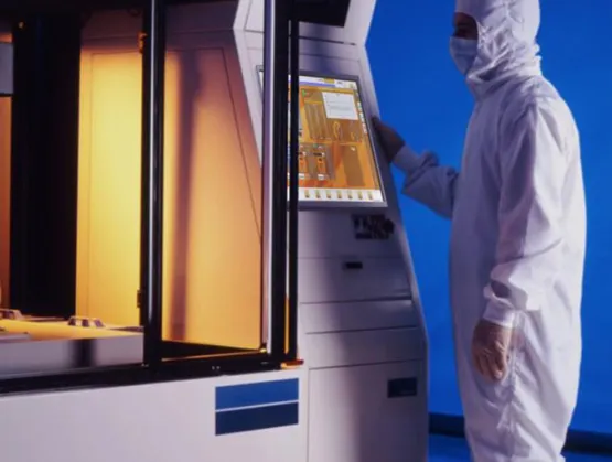
The semiconductor industry's approach to equipment automation has evolved from early serial interfaces to modern, data-centric architectures. From the early SECS/GEM standards to the GEM300 suite and the more recent Equipment Data Acquisition (EDA) suite, all efforts reflect a deeper level of automation, standardization, and data richness. This approach shows both alignment with global trends, and at times, deliberate divergence to address domain-specific requirements.
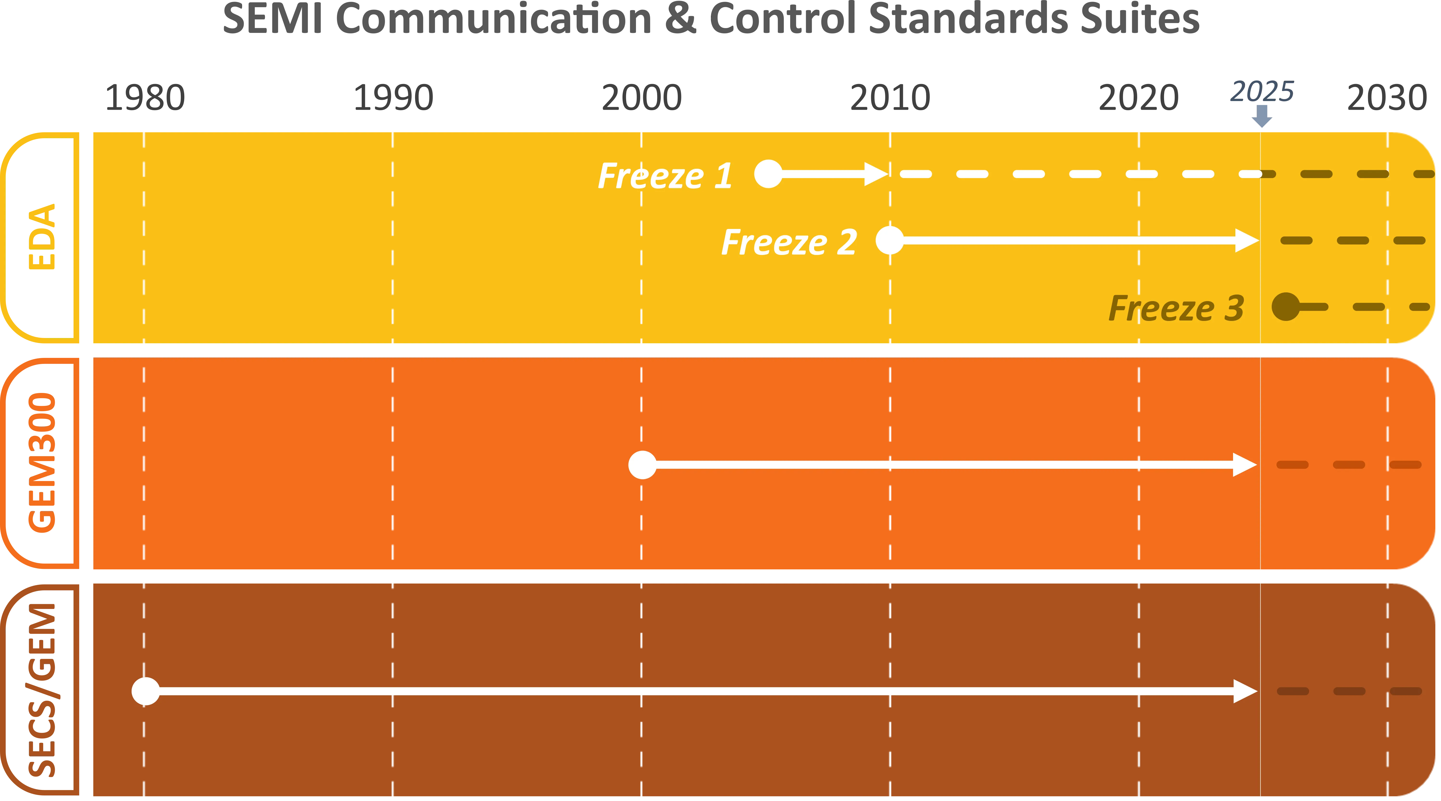 In the 1980s, SEMI introduced the SECS-I and SECS-II standards, which enabled structured communication between manufacturing equipment and host systems. SECS-I focused on physical connections, initially using the serial RS-232 protocol, while SECS-II defined standardized messages for event reporting, status updates, and command execution. At that time, other industries mostly operated with proprietary protocols, though Modbus had emerged as an open, widely adopted serial protocol for Programmable Logic Controllers (PLCs). However, there was limited convergence in higher-layer communication models, and factories generally consisted of isolated systems with minimal integration.
The early 1990s saw the introduction of the Generic Equipment Model (GEM) standard, which brought greater maturity to the semiconductor communication landscape. Built on SECS-II, GEM introduced structured states, events, and behaviors, making it easier to integrate and control equipment consistently across vendors. GEM effectively enforced a uniform interaction pattern, enabling semiconductor fabs to achieve better interoperability. During this same period, other industries began formalizing their own frameworks. For example, ISA-88, released in 1995, introduced modular batch process control models, and OLE for Process Control (OPC) offered a Windows-based, vendor-neutral standard interface for accessing device-level data. While these initiatives complimented GEM in spirit, they had a different focus. GEM specified behavior and interaction rules, whereas OPC initially addressed data access layers without enforcing equipment behavior.
By the late 1990s, the semiconductor manufacturing industry was transitioning from 200mm to 300mm wafers, which demanded significantly more automation and coordination. To address these demands, SEMI introduced the GEM300 standard suite, extending GEM to cover advanced topics such as carrier management, substrate tracking, and process job execution. Standards such as E87, E90, and E94 became essential for fully automated 300mm fabs. GEM300 stood out not only for its functional scope, but also because compliance became mandatory for semiconductor equipment vendors. These requirements ensured a level of standardization and integration discipline that few other industries could replicate at the time.
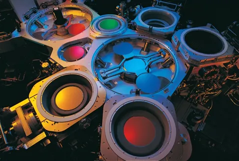 Semiconductor Multi-Chamber Cluster Tool |
Although the GEM300 advanced automation control in fabs, the need for richer, high-volume data collection became apparent in the 2000s. SECS/GEM interfaces, which were optimized for event and state messages, were not well suited for high-frequency sensor data or complex analytics. In response, SEMI developed the EDA standards, also known as Interface A, which introduced a parallel communication channel alongside GEM specifically designed for structured, high-throughput data access. Using the web technologies available at the time, including SOAP/XML over HTTP, EDA enabled factory systems to subscribe to live data streams and query metadata about equipment models, sensors, and events.
The EDA initiative reflected the same architectural shift seen in broader industrial automation during the 2000s. The introduction of OPC Unified Architecture (OPC-UA) in 2006 marked a similar leap forward. Unlike its predecessor, OPC-UA was not dependent on Windows and introduced secure, cross-platform, service-oriented communication. Like EDA, it supported information modeling, enabling machines to describe their structure, capabilities, and data points in a standardized format. The convergence of metadata-driven interfaces, platform neutrality, and secure, service-based communication indicated that the semiconductor industry's data needs were part of a broader transformation in how factories operate, instead of an isolated phenomenon.
SEMI diverged from broader industrial practices in making this transition by maintaining two distinct communication channels in parallel. SECS/GEM extended through GEM300 and remained the standard for equipment control, basic state reporting, and process coordination. Conversely, EDA became a dedicated channel for high-speed, high-bandwidth data access. This dual-path strategy enabled semiconductor fabs to maintain the reliability and maturity of SECS/GEM-based automation while facilitating more flexible and scalable data acquisition through EDA. Many other industries, in contrast, aimed to unify these functionalities within a single protocol stack, such as OPC-UA, which evolved to handle both command and data semantics.
However, the rate and scope of adoption differed between the semiconductor and general manufacturing sectors. Semiconductor fabs benefited from strict standard enforcement. Procurement contracts often mandated compliance with SEMI standards, accelerating uniform implementation. In contrast, other industries had to contend with legacy systems, vendor fragmentation, and less centralized enforcement. This resulted in a more gradual adoption of technologies. Although conceptually aligned, broader industry standards tended to offer flexibility and generality rather than the prescriptive depth seen in the semiconductor sector.
By the 2010s, the push for digital transformation, predictive analytics, and machine learning had placed new demands on communication infrastructure. SEMI’s EDA framework began to show its age due to the performance limitations inherent in SOAP and XML. Meanwhile, RESTful APIs, JSON, and lightweight publish-subscribe (pub-sub) models were becoming the norm in IT, and increasingly, OT environments. OPC-UA added support for MQTT and UDP-based pub-sub messaging, and many manufacturers started using cloud-native communication frameworks for telemetry and remote monitoring.
Recognizing the need for modernization, SEMI initiated EDA Freeze 3. This update replaced XML and SOAP with HTTP/2 and gRPC and uses protocol buffers for compact, efficient data serialization. Originally developed for high-performance web and cloud systems, these technologies significantly reduced latency and bandwidth usage. EDA Freeze 3 effectively aligns semiconductor data acquisition infrastructure with the latest IT paradigms. This mirrors the direction taken by leading manufacturers in other sectors who are beginning to explore gRPC, microservices, and streaming architectures as part of their factory modernization efforts.
Despite this alignment, SEMI standards remain distinct in their specialization. They are tailored specifically to the needs of high-mix, high-precision, and high-throughput semiconductor manufacturing. This focus enables them to define precise control and data behaviors; however, it also makes them less transferable to other industrial domains. General standards, such as Ethernet/IP, ProfiNet, and OPC-UA, were designed with cross-sector applicability in mind. As such, they evolve with broader consensus, but they often lack the specificity required for the complex integration scenarios found in semiconductor fabs.
The rise of AI, digital twins, and cloud-based control frameworks across industries is pushing everyone toward data-driven, interoperable systems. Whether the payload is a command for a lithography tool or a vibration stream from a packaging robot, the principles are converging. Communication standards must now be interoperable, contextual, secure, and scalable.
In conclusion, the evolution of SEMI standards reflects a domain-specific response to challenges in semiconductor manufacturing and broader participation in global industrial trends. From SECS/GEM to GEM300 and now EDA Freeze 3, each step has paralleled broader movements in industrial communication, often anticipating or reinforcing them. The result is a mature, high-performance communication stack that shares architectural foundations with its counterparts in other sectors, while preserving the specialization that makes it effective for the semiconductor industry.
About Dr. Fahad Golra
 As Director of Product Innovation for Agileo Automation, Dr. Fahad Golra drives next-generation solutions in connectivity, data modeling, and communication architectures. Since joining the company in 2019, he has been a key force behind Agileo’s push toward Industry 4.0, championing interoperability, digital twins, and edge-to-cloud systems. With 15 years of experience spanning academia, research, and industry, Fahad brings deep technical insight and thought leadership to the semiconductor industry. An active contributor to SEMI and the OPC Foundation, he’s a frequent speaker at global industry events and a published author advancing the dialogue around smart manufacturing and automation.


