
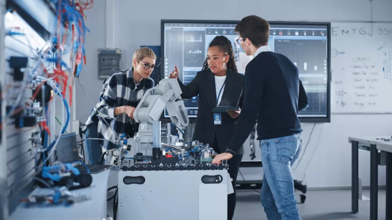
Unlock the Power of In-Person Learning
As valued talent development professionals, you understand the importance of investing in your team's skills and knowledge. That's why SEMI University is excited to partner with PT International, LLC to bring our comprehensive training programs directly to your doorstep. Our on-site training solutions provide a unique opportunity for your team to learn from semiconductor industry experts in a personalized and interactive environment.
We offer a range of courses suitable for groups of 10+ attendees. Choose from our standard curriculum or work with us to create a customized training program that meets your specific needs.
Maximize Your Impact: The Benefits of On-Site Training
- Increased Engagement: Face-to-face interactions with instructors and peers foster a more engaging and effective learning experience.
- Customized Content: Our courses can be tailored to meet your company’s objectives.
- Cost-Effective: Reduced travel costs and increased productivity make on-site trainings an attractive option for large groups.
- Flexibility: We can accommodate your schedule and preferences to ensure minimal disruption to your operations.

Webinar Option
If on-site training isn't feasible, we also offer webinars as an alternative. Our experienced instructors can deliver high-quality virtual training sessions tailored to your company's requirements.
Build the team you need to ensure long-term competitiveness and close the talent gap. Explore our course offerings and contact us today to schedule an on-site training that meets your needs and enhances your organization's performance.
Fundamental Semiconductor and Electronic Courses
Course Description (1 Day): This course introduces basic electronic concepts such as current, voltage, resistors, capacitors, inductors, diodes, and transistor fundamentals. Essentially, this course covers all that you need to know to get started in the electronics and semiconductor industry.
Course Description (3 Days): This highly interactive, hands-on course teaches learners how to troubleshoot basic electronic problems. Basic electronic concepts will be taught, and learners will be provided materials in the training to support the completion of learning objectives. Class size is limited to 14 students.
Course Description (1.5 Days): The purpose of this course is to provide a comprehensive understanding of the semiconductor industry and the manufacturing process of an integrated circuit (IC). The course is designed for new personnel entering the field or individuals who are looking for a well-rounded understanding of all the jargon, tools, and materials used in the IC manufacturing process.
Course Description (1 Day): Embark on a journey through semiconductor design, manufacturing, and business in this illuminating course. Explore IC design techniques, transistor evolution, and market dynamics. Delve into substrate types and industry economics, discovering the fastest-growing markets and key players shaping the semiconductor landscape.
Course Description (1 Day): Discover the essential secrets behind semiconductor devices! Dive into the intricate world of integrated circuit fabrication and design with our comprehensive course. Ideal for both technical and non-technical professionals, this training has been a cornerstone for the industry for over four decades, attracting over 120,000 eager learners since 1978. Join us and equip yourself with the vital knowledge needed to thrive in the semiconductor industry.
Course Description (1 Day): This course covers patents and intellectual property concepts that are important for technology companies to be informed of. By taking this course, you will gain an understanding of the different type of intellectual properties (IP), associated terms, the patent filing process for both US and international markets, and insight as to how to patient inventions. If you’re an industry member who wants to learn more about trademarks, copyrights, patents, and other legal rights related to technology innovations, this is a great course to take.
Course Description (1 Day): This course is about the device yield-related aspects of the Silicon Wafer. It is designed to give engineers working in yield improvement, as well as all process engineers and others who are involved in specifying Silicon in IC and MEMS devices, a working knowledge of the defects associated with the Silicon that arise from the vendor as well as those generated through device processing. Throughout the course, practical knowledge of specific silicon defect and yield-related manufacturing examples will be introduced through a series of short, one page "Applications Notes" covering topics of interest.
Course Description (1 Day): This 2-day course will use real-world case studies to provide detailed insights into MEMS markets, products and technologies. In addition to reviewing MEMS devices and their materials and fabrication technologies, other topics such as interface circuits, packaging, test and reliability and product qualification are covered in a practical manner that can be used as a foundation for successful a product development effort.
Course Description (1 Day): This introductory course is designed to educate people from any background on the exciting new technologies and markets being developed in MEMS. The course begins with basic fabrication technologies, including traditional methods and the latest techniques. Next is an explanation of the governing equations of these devices, where many things are different from macro-scale electromechanical systems. Fabrication and design are illustrated with examples of existing and future products in inertial sensors, optical fiber switching, displays, and sensor networks.
Course Description (1 Day): This course will equip attendees with the necessary knowledge and skills to contribute to more sustainable practices in the semiconductor industry. It covers the fundamental steps involved in semiconductor wafer processing. Specific health hazards and environmental effects of semiconductor manufacturing, and techniques and technologies for reclaiming and recycling materials and resources, and best practices for reducing the environmental footprint of semiconductor fabs.

Semiconductor Fabrication Courses
Course description (1 Day): This course introduces learners to atomic layer deposition (ALD) and its purpose in semiconductor manufacturing. ALD tools, gases used in ALD, the operations of ALD, the operations and processes of ALD are also discussed. Towards the end of the class, learners can also discover emerging technologies and technological trends related to ALD. If you’re looking to learn more about ALD and all topics related, this training is highly recommended!
Course Description (2 Days): This 2-day introductory course provides maintenance, equipment engineers, and technicians with a basic working knowledge of radio frequency (RF) technology as it is applied to semiconductor processing equipment. The role of RF in the various deposition processes, including sputter deposition and etching systems, is discussed. The characteristics and uses of various components that make up an RF system are described. The differences between resistive and reactive components and series and parallel resonance are explained. The course also covers tuning circuits, filter circuits, and the plasma chamber itself.
Course Description (2 Days): This 2 day introductory course provides maintenance, equipment engineers, and technicians with a basic working knowledge of radio frequency (RF) technology as it is applied to semiconductor processing equipment. The role of RF in the various deposition processes, including sputter deposition and etching systems, is discussed. The characteristics and uses of various components that make up an RF system are described. The differences between resistive and reactive components and series and parallel resonance are explained. The course also covers tuning circuits, filter circuits, and the plasma chamber itself.
Course Description (1 Day): This one-day course provides a working knowledge of surface conditioning and cleaning techniques used in the manufacture of integrated circuits. Fundamentals of the techniques used for cleaning the wafer surface will be discussed. Practical applications and methods for cleaning will be presented. Upon completing this course participants will have an understanding of all types of cleaning processes used in IC manufacturing; surface conditioning for pre-diffusion clean, in particular pre-gate oxide clean, post-etch and post-implant photoresist removal, particle removal, post-CMP clean. Participants will be able to understand the cleaning roadmaps and limitations of clean technologies as the node sizes decrease. The course participant should be able to make informed decisions on the surface conditioning and cleaning processes and techniques to utilize for IC manufacturing.
Course Description (2 Days): This 2-day course is designed for the semiconductor manufacturing employees to better understand SPC, control charts and the impact on quality and business. The course will teach the basics of creating control charts, implementing them into production and appropriate action for out-of-control conditions.
Course Description (3 Days): Elevate your skills and transform your approach to process improvement with our one-day Design of Experiments (DOE) workshop tailored exclusively for process technicians! Embark on a dynamic learning journey to empower you with the tools to conduct impactful experiments. From understanding the fundamentals of experimental design to hands-on experience in executing experiments, this workshop is crafted to elevate your expertise in a way that directly translates to real-world success.
Course Description (1 Day): This course provides attendees with an overview of the fundamentals, status, and technical challenges of EUV Lithography. It begins with a review of lithography in general drawing parallels between EUV and DUV lithography. The course then covers EUV specific challenges/solutions including sources (lithography and metrology), optics, metrology, masks, and patterning materials. Two areas where EUV specific challenges are particularly significant are patterning materials and photomasks; this course will cover these two areas in more detail including topics such as resist stochastics, radiation chemistry, reflective thick masks, off-axis mask illumination, phase shift masks, and mask stochastics. The course is intended to be a general overview and the deeper dive topics of resist, and masks will also be kept at the generalist level making the course accessible to a broad technical audience.

Assembly & Packaging Courses
Course Description (1 Day): This one-day course provides an overview of fan-out packaging. Key concepts, advantages, the history, processes, are discussed.
Course Description (2 Days): This course provides industry professionals with an understanding of flip chip interconnection and packaging. By partaking in this training, you will walk away with a solid understanding of the fundamentals of Flip Chip technology and where it is used in semiconductor field.
Course Description (2 Days): This course addresses IC packaging, assembly, and chip/substrate interconnections. It stresses the impact of the IC and end product requirements, i.e., “smaller, better, cheaper” and their influence on the manufacturing processes.
Course Description (2 Days): This course addresses IC packaging, assembly, and chip/substrate interconnections. It stresses the impact of the IC and end product requirements, i.e., “smaller, better, cheaper” and their influence on the manufacturing processes. Topics include all types of packages including ball grid arrays, flip chip, fanout, leadframe, stacked die, stacked packages, System-in-Package, and chip scale packages, and assembly technologies – Chip & Wire, Tape Automated Bonding, and Flip Chip. The growing importance of packaging as a way to deliver high integration and performance in today's products through heterogeneous integration of chiplets or 3D hybrid bonding will be discussed.

Business Skills for the Semiconductor Professional
Course Description (1 Day): In today’s fast-paced and dynamic business environment, the ability to manage projects with precision and efficiency is crucial. This course, inspired by the gaps identified in existing study materials, is tailored for both current and aspiring project managers seeking success in assignments, industry and certification exams like the Project Management Professional (PMP). The course offers comprehensive guidance that combines technical and managerial processes, applicable across diverse industries such as Semiconductor, Engineering etc. Key tips promote SMART and efficient study methods, helping the targeted audiences excel in mindset and scenario-based questions.
Course Description (1 Day): This course provides an in-depth exploration of the semiconductor supply chain, highlighting the
constraints caused by geopolitical issues, global disruptions, natural disasters, raw material shortages, and industry accidents. It explains the significance of the secondary (gray) market and offers strategies to minimize reliance on it through effective inventory management, scheduled shipments, and approving alternative components.

Production Testing Courses
Course Description (1 Day): The course will cover the basic segments of today's high volume production test as found in Outsourced Assembly And Test contractors (OSATs), as well as internal Integrated Device Manufacturers (IDMs). Participants will learn basic, but powerful, aspects about the semiconductor industry.
Course Description (1 Day): This course covers the basic economics of testing as found in Outsourced Assembly and Test contractors (OSATs), test equipment & service providers, as well as the end customer – the internal Integrated Device Manufacturers (IDMs).
Course Description (1 Day): This course will teach you how to choose appropriate test equipment: ATE & SLT systems, the handler or prober. You’ll also learn to choose the appropriate systems that meet the requirements for testing the semiconductor component without being too expensive. Lastly, topics related to testing hardware are also covered.
Course Description (1 Day): This course teaches how to optimize test flows. During a semiconductor product life cycle, there is a launch into high volume production test that provides sufficient test coverage to meet customer requirements, yet still meet cost targets. Packaging and test are closely linked – given various form factors & complexities (wafers, panels, strip, partially or fully packaged parts) and distributed test flows.