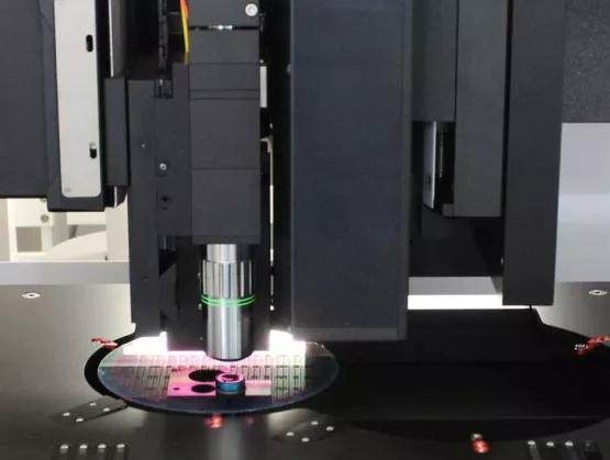
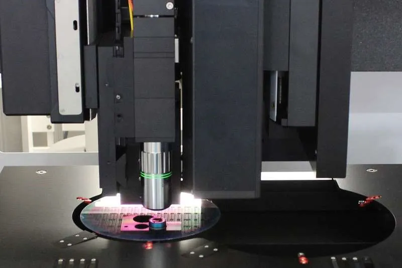
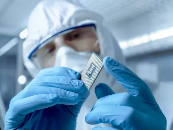
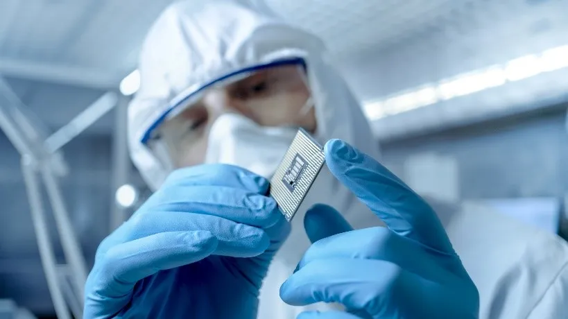
Imagine a world where there are chips in about everything we touch on a daily basis. It is not hard to do with semiconductors already at the core of many leading-edge electronic devices. These sophisticated chips are hidden from sight, but their functions are vitally significant to our daily lives.Manufactured in multibillion-dollar facilities, the production process of chips is one of the riskiest, costliest, and most technically complex feats in business. Consider the difficulties of managing contaminants during device manufacturing: A single speck of dust on a lens could cause the entire output of the plant to be scrapped.For years, these exotic fabrication facilities, called fabs, have been packing more efficiency into ever smaller chips. As new technologies continue to emerge, chip manufacturers face constant pressure to continually refine and improve their operations to meet the challenge of rising device performance and yield goals. Fab managers must optimize tool performance, improve fabrication techniques, safely handle toxic materials and design better integration flows. Layer on top of those requirements customer demand for greater innovation and quality of service, it can be difficult for manufacturers to handle everything on their own while consistently meeting necessary requirements.Align for CollaborationWith the help of the Fab Owners Alliance (FOA), a SEMI technology community, manufacturers and their suppliers don’t have to travel this road alone. Membership in this international group allows semiconductor and MEMS fab managers and industry suppliers to come together to solve common non-competitive manufacturing issues and improve business results.Founded in 2004, the group consists of 25+ device manufacturers (DMs) with over 120 semiconductor manufacturing facilities and 60+ solution providers (SPs) who supply equipment and services. Through quarterly meetings, study teams, benchmarking surveys, case studies and online forums, FOA successfully provides a collaborative, non-competitive platform to the fab management and operations community. FOA members enjoying an engaging discussion and networking event during the recent Q1 2019 Collaborative Forum at the Double Tree Resort in Scottsdale, Arizona One of the most popular FOA platforms is the annual Collaborative Forum early in the year. The goal is to bring together DMs and SPs from around the world for an open dialogue under one roof. For two days, they share success stories and discuss issues facing their fabs and the industry in general and develop collective strategies to address them.The success stories are particularly engaging as they accentuate the value and benefits of FOA membership. Presented as case studies, these stories outline how the DMs and SPs work together to improve fab efficiency and increase yields. Often, the ideas for the case studies are conceived during networking events, fab tours and programs organized by the FOA.The case studies shared at the 2019 Collaborative Forum, held at the Double Tree Resort in Scottsdale, Arizona, February 13-14, 2019, illustrate the power of collaboration within the FOA. Following are a few examples.Scheduling System Implementation Broadcom was facing a steep ramp when it decided to engage with FPS, an INFICON product line. In addition, the manual decision making, and limited real-time visibility of factory data was negatively impacting their production in its 150mm and 200mm environment. By deploying an integrated Smart Manufacturing software solution and its digital twin, FPS was able to retrofit Broadcom’s manual factory with automated decision-making capabilities.This solution offered many benefits. Constraint tool utilization increased by more than 15 percent. The automated WIP management system also eliminated many manual wafer handling issues such as lost lots, WIP storage constraints, building transfers, and time spent looking for lots. Pushing Tool Performance BoundariesAs tools in the 200mm space are hard to find, GLOBALFOUNDRIES is always looking to squeeze every wafer out of its existing resources. To drive continuous improvement and increase equipment throughput, GLOBALFOUNDRIES leveraged MAX’s knowledge with Machine Rate Models. Together, they were able to employ a modelling technique that helped them model key toolsets and develop actions to increase intrinsic machine rate performance.Based on this knowledge, 10 capacity constraints were selected, and speed models were developed for all of them. This win-win collaboration allowed GLOBALFOUNDRIES to find some real opportunities that translated into CAPEX and cost savings. On average, the companies identified a 12 percent potential improvement opportunity per toolset and created engineering task force teams to prioritize and drive the improvements.Simplifying the Chamber Matching Process Using Trace AnalyticsThe collaboration between NXP and BISTel resulted from a shared vision of achieving Smart Manufacturing using analytic solutions enabled by artificial intelligence and other advanced technologies. Chamber matching is critical in identifying process variation to ensure manufacturing quality. Traditional tools like Fault Detection Classification (FDC) often do not provide clear enough insights to pinpoint the issues and require extensive time to collect data from each chamber.Through several use cases, NXP and BISTel successfully illustrated the effectiveness of using a trace analytic solution to quickly and accurately quantify and monitor chamber-to-chamber mismatches as well as changes within a chamber over time. The full trace analyses of all parameters allowed NXP to generate better FDC models to more quickly detect similar issues in the future. In addition, NXP was able to identify the cause of a parametric shift by comparing performance of the same chamber between two different time periods. All in all, the trace analytics solution brought together and analyzed the process data efficiently, thereby reducing analysis time from days to minutes.Eagleview Inspection of SiC and Transparent Wafers X-FAB challenged Microtronic to develop a new capability for its high-throughput recipe-less macro defect inspection systems. Microtronic’s EagleView machine vision macro defect inspection system is well known for its versatility in the semiconductor industry due to its wide deployment as well as its recognition as winner of the 2017 Best of West Award at SEMICON West. But X-FAB’s requirements to inspect and image transparent wafer substrates were novel. After working closely to understand X-FAB’s needs, Microtronic made extensive hardware and software enhancements to enable high-throughput macro inspection of Silicon Carbide (SiC) and other transparent wafer substrates.Get InvolvedThe FOA meetings are held at device manufacturing sites twice a year. The next meeting will be graciously hosted by MACOM in Lowell, Massachusetts, May 22-23, 2019. The DMs and SPs will meet again at SEMICON West at the Moscone Center in San Francisco on July 11, 2019.To attend these meeting and be part of this high-impact group, please email us at [email protected]. For more information about FOA, please visit our website.Nishita Rao is a marketing manager at SEMI.