downloadGroupGroupnoun_press release_995423_000000 copyGroupnoun_Feed_96767_000000Group 19noun_pictures_1817522_000000Member company iconResource item iconStore item iconGroup 19Group 19noun_Photo_2085192_000000 Copynoun_presentation_2096081_000000Group 19Group Copy 7noun_webinar_692730_000000Path
Skip to main content
Default Banner Image

sensors

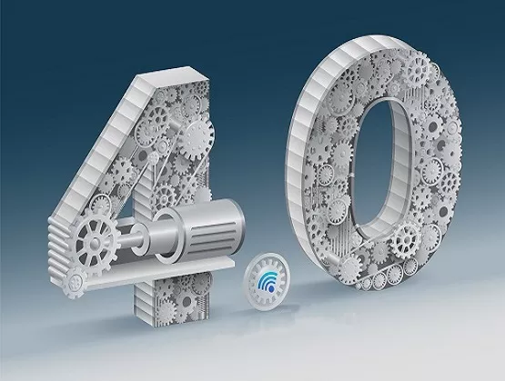
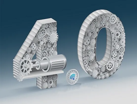
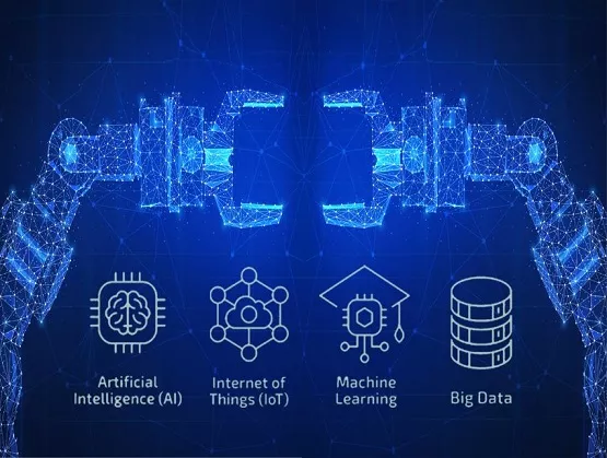
Demand for hi-tech manufactured goods is at an all-time high and is expected to grow significantly in our new digital age, COVID-19 economy. This is especially true for semiconductor chips. Chip manufacturers have been working to meet this demand by building new factories and by optimizing processes and equipment in existing fabs. While there is much media coverage about new factories planned by leading-edge chipmakers and government investments in the semiconductor sector, greenfield fabs entail significant capital expenditures and are sometimes fraught with complex political concerns. As a result, they can take several years to complete and reach their planned production capacity. Instead, the semiconductor industry needs to optimize existing factories in order to increase productivity and yield and meet growing demand by implementing smart manufacturing solutions. Smart manufacturing solutions will inherently reduce costs with more efficient and automated processes, and those savings can be reinvested for the next wave of solutions. Chip Industry on the Bleeding Edge Semiconductor manufacturers have always been focused on bleeding-edge technology to outflank strong competition and build the best products – faster and cheaper. Today, pioneering organizations are using data to optimize manufacturing processes and equipment, a practice known as Smart Manufacturing. While there are many definitions of Smart Manufacturing, the essence is maximizing the utility of big data generated in these factories by leveraging three pillars: Sensing, Connecting, and Predicting. It is not just the digitization in manufacturing, but it is also about turning the data into actions that generate value – an effort the SEMI Smart Manufacturing Committee is driving based on the three pillars. Optimizing return on investment is the ultimate goal. SEMI Smart Manufacturing Initiative activity is based on three pillars that support the goal of increasing ROI. Making the Right Decision, Faster Smart manufacturing practices enable organizations to make the right decisions and take action faster based on insights generated from real-time and historical data. This requires data management technologies and applications that can process, analyze, and act on information instantly. It has become ever more difficult to process and discern the relevant data or signal from the vast volume of data, perform analytics or develop new ML or AI analytic tools, and then make the critical decisions to solve problems as close to real-time as possible. Who’s Responsible – IT or OT? In the past IT (Information Technology) and OT (Operations Technology) were separate entities within organizations, with IT focused on storing large amounts of data for enterprise systems and OT concentrated on using data to perform specific functions. Smart Manufacturing often demands combining IT and OT, difficult in rigid organizations that operate the two organizations independently and lack the infrastructure to implement comprehensive solutions. Success requires executive leadership sponsorship, motivated technical personnel and, most importantly, a clear deliverable on the value in implementing Smart Manufacturing. Many organizations have introduced top-level leadership positions such as a Chief Information Officer or Chief Data and Analytics Officer to address this convergence and many of these leaders are embracing Smart Manufacturing practices. The SEMI Smart Manufacturing community includes many of these leaders and therefore has highlighted the importance in the return on investment for Smart Manufacturing solutions. Read more about IT and OT convergence and note that Smart Manufacturing is synonymous with Industry 4.0. The SEMI Smart Manufacturing Initiative covers the entire supply chain. Get Smart in Smart Manufacturing While new technologies and applications are being created to deal with mountains of data, it is the underlying methodologies and practices that are key to a successful Smart Manufacturing deployment. SEMI, the trade association representing the electronics manufacturing and design supply chain, is in a perfect position to evangelize Smart Manufacturing experiences and best practices for the entire manufacturing community. The more than 30 member companies participating in the SEMI Smart Manufacturing Initiative bring more than 500 years of collective experience and knowledge to the topic. Many segments of the supply chain participate in the SEMI Smart Manufacturing Initiative including packaging, assembly, SMT and PCB assembly, test, software, data management, sensor and material suppliers. Learn How to Manufacture Smarter SEMI SMART Manufacturing is hosting two great conferences in the coming months – the Global Smart Manufacturing Conference (GSMC) and the SEMICON West Smart Manufacturing Pavilion. As a leader of the organizing committee and chair for the SEMICON West Smart Manufacturing Pavilion, I encourage people who want to learn how to implement Smart Manufacturing or expand their knowledge of Smart Manufacturing to attend these events. The GSMC will feature keynotes highlighting the value of Smart Manufacturing, offer tutorials on the three pillars, and introduce several case studies for each of the pillars. Thirty-two organizations – ranging from global cloud providers, semiconductor factory operators, leading equipment vendors and software application solution companies – will present. See the full agenda here. The SEMICON West Smart Manufacturing Pavilion will compliment GSMC by showcasing a number of use cases that highlight the value of Smart Manufacturing. Panel discussions will deep dive into the challenges of implementing these best practices and the direction smart manufacturing is taking in the coming years. Our goal for these events is for you to take this knowledge back to your companies, implement and improve on the detailed solutions highlighted at the conferences, and return next year to share your success stories with the community. See you soon, in person or virtually! About the Author Bill Pierson is VP of Semiconductors and Manufacturing at KX, leading the growth of streaming data analytics in this vertical. Bill is also a chair for the SEMICON West Smart Manufacturing Conference and an active team member of the SEMI Americas Chapter. He has extensive experience in the semiconductor industry including previous experiences at Samsung, ASML and KLA. Bill specializes in applications, analytics, and control. He lives in Austin, Texas, and when not at work can be found on the rock-climbing cliffs or at his son’s soccer matches.
Read More
Areas packed with dense foliage. Mile-deep mines and tunnels. Urban canyons. Indoor environments. Global Positioning System (GPS) technology has long been a boon to location tracking of aerial, terrestrial and aquatic vehicles — as well as to people in motion — but in many cases it can’t function with a high degree of reliability, either because the GPS signal is somehow obstructed, or worse, is jammed or spoofed. Delivering higher precision and higher reliability in GPS-denied environments — as well as immunity to jamming and spoofing — positioning, navigation and timing (PNT) represents the next evolutionary step in location positioning and tracking. With PNT so critical to a range of defense, commercial and industrial applications — and with sensors the building blocks of PNT solutions —the MEMS Sensors Industry Group, a SEMI Technology Community, is ensuring that our members play a transformative role in PNT innovations. We’ve secured $14.9 million in research dollars for PNT R D over the past 18 months, marking Phase I of a project funded through a public-private consortium with the U.S. Army Research Laboratory (ARL). With the typical funding structured as a 50/50 cost share with the industry participant, the research dollars go farther, and the level of commitment that each recipient makes is more pronounced. As we look ahead to Phase II of the MSIG PNT R D project, the details of which we’ll announce later this year, we’d like to reflect on the companies and research labs that won bids through a competitive process supported by the SEMI-MSIG PNT Technical Advisory Council and the SEMI-MSIG PNT Governing Council. Winners submitted proposals that both met our criteria for advancing PNT technologies relative to mobility, size and weight, and that laid a path toward greater cost efficiency and lower product price. “PNT doesn’t displace GPS,” said Tim Brosnihan, executive director of SEMI-MSIG. “Rather, getting the two technologies to work together improves position and tracking. While current PNT solutions use inertial measurement units, or IMUs, to effectively maintain positioning accuracy in the absence of a GPS signal, it’s also true that accumulated bias and noise-related errors in the IMUs make positional determination unreliable. Like most great pairings, GPS and PNT can work together. We can use IMUs when GPS is unavailable, and when GPS returns, it can be used to reset the IMU errors. So when the GPS signal is lost again, the IMU can maintain navigation and location. “We’re focusing this PNT project on technologies that will allow accurate positional determination in the absence of a reliable GPS signal for prolonged periods,” added Brosnihan. Here are snapshots of the 10 companies and research institutions that won awards for their PNT-focused developments. Analog Devices is developing an optimal size, weight, power, and cost (SWaP-C) solution for applications requiring high-accuracy navigation and uncompromised reliability. The company’s mode-matched navigation-grade gyroscope with system ID leverages an innovative sensor and its associated process design, a robust high-volume manufacturing flow, and system-control algorithms to achieve very high-performance (0.01 degree/hour bias instability and 0.005 degree/√hr angle random walk). Carnegie Mellon University (CMU) is developing a CMOS MEMS high-stability accelerometer through machine learning (ML). If embedded in footwear, these ML-optimized accelerometers could be used in personal navigation. If embedded in a golf ball, baseball or hockey puck, the accelerometer could extract the trajectory of the object in motion by measuring its shock (force). The CMU device validates state-of-the-art performance of the university’s high-dynamic-range accelerometer systems-on-chip. It also validates and tests ML models by measuring the accelerometer and auxiliary sensor output over long time periods (e.g., 1 hour, 10 hours, days) to collect independent long-duration time-series data. By modeling drift from environmental influences — along with possible overall system changes from extreme events, such as high-temperature excursions and shock — designers can dramatically reduce navigation errors to support more accurate navigation over longer time periods. GE Research is developing a novel MEMS gyrocompass that will enable high-end north-finding systems, traditionally unaffordable for automotive and consumer applications. The device will be available in mass-market applications such as robotics and autonomous vehicle navigation in GPS-denied environments. The MEMS gyrocompass enables a 10x reduction in SWAP-C with high accuracy. An additional benefit of this work is that GE will offer a foundry service process development kit (PDK) for its Polaris MEMS process, speeding the development and manufacture of MEMS devices in an advanced processing facility. Georgia Institute of Technology is developing high-aspect-ratio monocrystalline silicon carbide-on-Insulator (SiCOI) MEMS devices that will reduce navigation angle errors, potentially making widescale pedestrian navigation available in mass-market applications such as smartwatches and smartphones. The platform for ultra-high-performance bulk acoustic wave (BAW) gyroscopes and timing resonators will feature material properties that allow a much better structural symmetry and a higher-resonant quality factor (Q) than silicon MEMS (Si MEMS). Honeywell is working to enhance the navigation accuracy of commercial and military vehicles in GPS-denied environments through an innovation that dramatically improves the performance of a MEMS IMU by both refining candidate ML algorithms, including recurrent neural networks (RNNs), and by combining deep neural network (DNN)-based calibration and sensor fusion algorithms. PARC is developing a new materials platform for photonic integrated circuits (PIC). Aluminum gallium nitride (AlGaN), an ultra-wide bandgap semiconductor, is epitaxially grown to produce single-crystal layers for fabrication of optical components, such as waveguides and micro-ring resonators for optical signal processing. The project includes design and fabrication of specialized laser diodes at wavelengths needed to probe qubits based on atomic ions (e.g., strontium and ytterbium). The new platform offers several benefits: low optical loss from the ultraviolet (UV) to infrared spectral bands excellent non-linear optical properties for efficient frequency-generation processes (e.g., optical frequency combs); and enabling technology to realize compact, field-deployable quantum systems for PNT applications, such as ultra-fast distance measurements, microcombs for optical atomic clocks, photonic radar, optical coherence tomography, and coherent communications — all applications that benefit from the lower cost and small chip size of these integrated photonic circuits By expanding its proprietary EpiSeal encapsulation process to include new materials and topologies, SiTime is developing low-impedance and low-noise MEMS resonators with an ultra-stable wafer-level package. Because these novel MEMS resonators are highly reliable and very compact — while using less power and providing lower RF noise — they’re ideal for 5G RF timing applications, IoT devices, and smart vehicles. Teledyne Scientific Imaging (CSAC project) is conducting a study to identify paths to reduce the cost of battery-operated chip scale atomic clocks (CSAC) that provide affordable precision timing for denied environments. The project goal is to identify viable paths of reducing cost by an order of magnitude, without sacrificing performance. In addition to exploring design and manufacturability solutions, project researchers are performing short loop experiments as proof-of-concept validation. Through a second award, Teledyne Scientific (IMU project) is advancing packaging and integration for compact, navigation-grade six degrees of freedom (DOF) MEMS IMUs. Featuring reduced bias instabilities associated with packaging stresses and ambient temperature influences, the Teledyne Scientific IMUs promote environmentally robust low-stress packaging of wafer-level vacuum packaged (WLVP) MEMS gyro resonators, facilitating a lower-cost, smaller and more accurate IMU for performance-driven PNT applications. Twinleaf is developing a new light source module ideally suited for integration directly into quantum sensors. This project integrates a bright, tunable distributed Bragg reflector (DBR) near infrared (IR) 795nm wavelength laser made by the project’s subcontractor (Photodigm) into a package that locks the laser to an atomic reference line in a microfabricated vapor cell. The laser module’s high-output intensity and low magnetic signature will enable breakthrough performance levels for Twinleaf’s magnetometer and other quantum sensors requiring the light source integrated into the sensor module. Request for Proposal for Phase II of SEMI-MSIG PNT Program Opens Q4 2021 SEMI-MSIG will accept request for proposal (RFP) submissions for Phase II of its PNT program starting in Q4 2021. This year, in addition to funding IMU and timing device projects, MSIG will also consider proposals on imaging-based navigation solutions. If you’d like to submit for Phase II, sign up to receive more information on the RFP by visiting SEMI’s R D Programs page. You can also connect with Paul Carey by email, [email protected] or LinkedIn. Paul Carey, Ph.D., is the director of the MEMS Sensors Industry Group. With deep domain expertise in X-ray imaging backplane platforms — and their supply-chain technologies such as flexible substrates, laser annealing for semiconductors and silicides, thin film transistors (TFT) for flexible OLED displays, and polysilicon-on-plastic TFT technology — Carey has held technical leadership positions at dpiX, Applied Materials, and Lawrence Livermore National Laboratory. He received a double-major B.S. from UC Berkeley in Electronical Engineering and Computer Science (EECS), and Materials Science and Engineering (MSE). Carey holds an M.S. in EECS from UC Berkeley and a Ph.D. in MSE from Stanford University.
Read More
Our home state of California has wilderness areas of extreme climates, from desert to high-altitude snow-capped mountains. Every year, people need rescue because they’ve ventured into the wilderness without proper training, or even essential gear, such as water or a warm parka. Many MEMS product development teams get a similar start. They undertake a challenging multi-year journey without enough of the most precious resource needed for success – enough money to finish. As a MEMS product development firm that's completed more than 400 projects, 25% of these with startup companies, we’ve been having many of the same conversations about the road to commercialization with MEMS entrepreneurs. Through that experience, we’ve seen a share of these entrepreneurs – many of whom come right from graduate programs or from outside the semiconductor industry – experience disappointing outcomes. And it’s not because of their technology. Rather, their lack of familiarity with electronic product integration and wafer-based manufacturing often influences a too-optimistic development plan that doesn’t factor in enough time and budget. As technologists, it was tough for us to see companies with promising young technologies struggle due to lack of planning or funding. We would like to see more entrepreneurs succeed, and that was the impetus for our new book, MEMS Product Development: From Concept to Commercialization, some highlights of which follow. Time and money What can MEMS startups do to pave the way for a successful commercial launch, particularly when a long period of scaling up manufacturing is often needed during the go-to-market process? Since money is usually a limited resource, it’s important to prepare a realistic development timeline supported by sufficient funds allocation from the start. As this is easier said than done, we’ve seen both startups and established companies make common financial blunders during MEMS product development. These include: Reserving inadequate funding for developing the entire MEMS product, including packaging, electronics and software Creating an unrealistic timeline for development, resulting in a cash-flow problem Only securing enough funding for the first run at a foundry when, in fact, numerous runs are far more typical Unplanned gaps of months or more between funding tranches, which slows momentum Based on our varied client experience, the engineering costs of developing a MEMS product of medium complexity to the point of validated foundry production (i.e., ready for mass production and product sales) requires on average four years and US$4 million. And that’s just for engineering. Business administration, sales, marketing and other company costs are additional. While it’s common to spend much more for more complex devices or product systems, it’s rare to spend less, unless you’re working with existing IP, such as a foundry process platform, which also could accelerate development time. Typical engineering-only budget required to develop a MEMS product through four stages of development, to the point of volume-production readiness. Reprinted with permission from MEMS Product Development: From Concept to Commercialization (Springer, 2021). Don’t go thirsty in the desert No one wants to get stranded in the desert without enough water, which is why it’s so important to carefully articulate your timeline and secure adequate funding before starting MEMS development. In MEMS development, just as in wilderness adventuring, things rarely go exactly as planned: Wafers break, engineers take a long time to debug, customers change their minds, and random events like storms (or a pandemic) disrupt supply chains. That’s why adding some buffer to your development timeline and your budget will sustain your company through the inevitable delays and setbacks. Plus, there’s generally a ripple effect to a delayed new-product introduction. A slower-than-predicted launch places a burden on a company’s finances because the fixed overhead costs of the entire organization will continue to consume cash while waiting for product launch. Not a lump-sum game Although you might wish to receive one big funding check when you get started, the reality is that investors and executives won’t provide the entire development funding in one sum. They give money in tranches, generally demanding you meet some pre-determined criteria or demonstrate set benchmarks before they’ll release more funds. To best manage tranche funding, a company must carefully plan and set their investors’ expectations for realistic outcomes in advance. A common crisis for startup companies occurs when investors only provide enough budget to execute the very first run at a foundry and then demand to see functional chips before providing the next tranche. However, the aim of the foundry’s first wafer run isn’t to produce working chips. It’s to begin the year-long process of setting up for high-volume manufacturing. The first wafers are unlikely to yield well, or at all, putting the startup at great risk with its frustrated investors. Setting investors’ and executives’ expectations correctly from the start, realistic budgeting and having regular communication about progress and upcoming needs all help to keep the money flowing. Any gaps in funding will waste valuable momentum, which ultimately leads to more expense and delay in the overall product development. It can become especially damaging when the wait for money forces the foundry to stop work, because processes go stale after a few months, and also during busy times, when your product could be sent to the back of the foundry’s queue. As experienced outdoors people know, to enjoy wilderness adventures, you need to plan where you’re going, anticipate common risks, and then prepare accordingly. It’s the same in MEMS product development. Having a good grasp of your timeline and realistic expectations about the funding required to reach commercialization are essential steps in a successful journey. Want to learn more about MEMS Product Development: From Concept to Commercialization (Springer, 2021)? Order the book based on A.M. Fitzgerald Associates’ extensive experience helping entrepreneurs and other innovators commercialize their MEMS devices. Alissa M. Fitzgerald, Ph.D., founded A.M. Fitzgerald Associates, LLC, a MEMS product development firm based in the Bay Area, California, in 2003. She has over 25 years of engineering experience in MEMS design and fabrication and now advises clients on the entire cycle of MEMS product development, from business and IP strategy to supply chain and manufacturing operations. Carolyn D. White, Ph.D., has a background in mechanics of materials and specializes in the design and fabrication of MEMS devices for a wide range of applications. She has additional experience in foundry transfers and technology strategic analysis, including of the evaluation of patent portfolios, feasibility studies, and cost/performance analysis. A.M. Fitzgerald Associates (“AMFitzgerald”) is longtime member of MEMS Sensors Industry Group®(MSIG), a SEMI technology community that connects the MEMS and sensors supply network in established and emerging markets to enable members to grow and prosper. Visit us today.
Read More
Air pollution is a serious public health issue worldwide with airborne hazardous substances such as volatile organic compounds (VOCs), particle matter (PM), and nitrogen dioxide linked to a wide range of adverse health conditions. According to the World Health Organization (WHO), “the combined effects of ambient (outdoor) and household air pollution cause about seven million premature deaths every year, largely as a result of increased mortality from stroke, heart disease, chronic obstructive pulmonary disease, lung cancer and acute respiratory infections.” There’s also an economic impact of air pollution. Related illnesses and loss of life cost billions of dollars in healthcare services globally. And while we might think that air pollutants are only present outdoors, we’re more exposed to them – and they’re more potentially dangerous – indoors, where higher concentrations of volatile organic compounds (VOCs) produced by paint and furniture are a major concern. The COVID-19 pandemic has only heightened our awareness of the air we breathe. With recent medical research showing that viruses may be transmitted by attaching themselves to airborne particles, indoor air quality (IAQ) monitoring is becoming even more important. As we turn to VOC sensors for IAQ monitoring, it’s important to note that not all VOC sensors are equal. The current crop of low-cost VOC sensors are primarily total VOC sensors. Generally based on electrochemical or metal-oxide transducers, total VOC sensors provide a “grayscale” image of IAQ, which doesn’t differentiate among different gases. This limits people’s ability to make informed decisions regarding the level of threat to their health, since not all VOCs are equally hazardous and don’t require detection at the same concentrations. In addition, total VOC sensor technologies don’t support PM detection. This forces end-device designers to either add a module of optical sensors or switch to a completely different system. While optical sensors provide excellent performance, particularly for PM detection, they’re much more expensive, as well as more complex, bulky and power-hungry. This makes them ill-suited to resource-constrained portable devices where cost, size and power are at a premium. FBAR-based IAQ sensors emerge The shortcomings of available technologies for IAQ sensors has boosted the development of alternative solutions that provide better performance – in terms of both sensitivity and selectivity – as well as greater versatility, lower cost and smaller size. Acoustic sensor technologies featuring the latest advancements in film bulk acoustic resonator (FBAR) sensors are emerging as a leading candidate. Sensitivity is important in VOC detection because certain hazardous compounds, such as formaldehyde, are dangerous at very low concentrations. As highly sensitive devices, FBARs are a MEMS equivalent of a weight scale, but instead of detecting kilograms or grams, they can sense femtograms, which are just one-quadrillionth of a gram each. FBARS work by putting a thin film piezoelectric material into a mechanical resonance through application of an AC electric signal (GHz range) to a pair of electrodes on either side of the film. This resonant frequency is sensitive to the mass attached to the electrode surface. Whenever the mass attaches to the active area of the sensor, it produces a frequency shift, and this shift is proportional to the mass attached on the surface. Another major benefit of this approach is selectivity, which allows a device to distinguish between different target molecules or species. By placing a layer of material on the sensor –which is the functionalization layer – FBAR sensors display high selectivity on targeted materials. This allows the consumer to distinguish among different VOCs instead of just measuring a mixture of VOCs that vary in toxicity. Unlike older IAQ sensing technologies, FBAR sensors support functionalization layers comprised of different materials, from metal oxides and polymers to more exotic options such as carbon nanotubes and graphene. This increased versality makes it easier to use FBARs for a variety of applications, ranging from gas sensors to medical sensors. Sorex Sensors’ FBAR sensor in a 3mm x 3mm ceramic package FBAR technology is a perfect match for IAQ. In addition to high sensitivity and selectivity, it enables the manufacture of very small arrays, and it’s low-power, all of which make it a good choice for small portable devices. Plus FBAR technology is CMOS-compatible, so FBAR sensors can be made using standard MEMS processes and combined with integrated circuits fabricated using standard CMOS processes, making them cost-effective. With its origins at the University of Cambridge in the UK, Sorex Sensors is leading the commercialization of FBAR devices for sensing applications. After releasing our first product in 2019 – a standalone FBAR sensor and a development kit that can be used for particle monitoring – we’re preparing to release an FBAR sensor array that detects five different gases later this year. By offering specific functionalization layers for different targets, our new FBAR technology will provide a level of selectivity that other silicon-based sensors can’t achieve – particularly in light of FBAR’s low power consumption and very small size (less than 5mm x 5mm). In addition, the sensor’s targeted gases will include one of the main headaches in the IAQ space, formaldehyde, which is especially carcinogenic and is widely found in the varnishes used in furniture. We’re planning for this new iteration of our FBAR technology to help our customers sense in color rather than in grayscale – providing a level of granularity that’s unmatched in IAQ sensing. Check out the latest news about Sorex Sensors on our website and on LinkedIn. About the Author Mario de Miguel Ramos, Ph.D., is the co-founder and CEO of Sorex Sensors Ltd, a spin-out of the University of Cambridge, the University of Warwick, and the Universidad Politecnica de Madrid (UPM). Founded in 2017, the company focuses on the development of highly sensitive mass sensors based on film bulk acoustic resonators (FBARs). Dr de Miguel Ramos has been working in the field of FBARs for a decade. Prior to founding Sorex Sensors, he worked as a postdoctoral research associate at the Electronic Devices and Materials (EDM) Group at the University of Cambridge. He holds a master’s in Telecommunications Engineering and a Ph.D. in Electronic Engineering Systems, both from UPM. Sorex Sensors is a member of MEMS Sensors Industry Group®(MSIG), a SEMI technology community that connects the MEMS and sensors supply network in established and emerging markets to enable members to grow and prosper. Visit us today.
Read More
What does it mean to identify as LGBTQIA+ in the semiconductor industry? It’s an interesting question to ask, but a difficult one to answer. Because we live in a world in which cisgender heteronormity is assumed, it’s possible to self-identify as LGBTQIA+ without sharing that information publicly. Coworkers and managers might not even realize that their colleague or employee is gay, lesbian, transgender, non-binary or other. Unlike other minorities, notably people of color, LGBTQIA+ people may choose to keep their identities invisible.As I began outreach for this article, I recognized that some people might not want to expose a potential vulnerability to both their co-workers and a broader global audience of SEMI members, so I tried to make them feel more comfortable. I told them I’m a lesbian. I said that I’d send content for their review before publishing. But I quickly discovered that wasn’t enough, despite sweeping cultural and legal advances around LGBTQIA+ attitudes and identity. According to a 2020 Gallup Poll, 5.6% of U.S. adults now identify as LGBTQIA+, up from 4.5% just three years ago. In 2004, Massachusetts became the first U.S. state to legalize same-sex marriage, and in 2015, the U.S. Supreme Court made same-sex marriage legal in all 50 states. The semiconductor industry has been historically conservative. The times, however, are changing. Large chip companies such as AMD, Intel and Lam Research actively support diversity and inclusion efforts across minority groups, including LGBTQIA+, and that’s a good thing, but is it enough? And if not, what actions can SEMI members take to help LGBTQIA+ people in semiconductors feel safe enough to choose visibility?According to Antoinette Hamilton, global head of Inclusion and Diversity at Lam Research, more than 46% of LGBTQIA+ employees in the industry aren’t out in the workplace. That tells us there’s still work to be done, a challenge that Lam is embracing. With its Pride employee resource group (ERG) leading the way, partnerships with organizations such as PFLAG and Out Equal, and recruitment efforts made through organizations such as Out in Science, Technology, Engineering, and Mathematics (oSTEM), Lam has earned a score of 100 on the Human Rights Campaign Foundation’s Corporate Equality Index and was named one of the Best Places to Work for LGBTQ Equality.“At Lam, we understand the importance of empowering employees to bring their authentic self to work,” says Hamilton. “We believe when employees feel valued and included, each person can reach their full potential.”Back in 1992 when Intel paid to relocate Judi Goldstein, her partner and their son from New Jersey to Oregon, mainstream cultural attitudes toward gays and lesbians were very different. According to a June 1992 Gallup poll, only 48% of Americans thought that “gay or lesbian relations between consenting adults should be legal,” with 44% saying they should be illegal. A May 2020 Gallup poll recorded a dramatic shift in attitudes, with 72% affirming the legality of same-sex relations and only 24% opposed.By the late 1990s, Intel had extended domestic partner benefits to same-sex couples. “I registered my partner – now my wife – and our son, and realized that from then on, my whole family would have health insurance through Intel,” says Goldstein, who identifies as a gay woman and uses she/her pronouns. “Both relocating my family and providing family health coverage solidified my attachment to Intel, which was way ahead of other companies at the time.”By 1995, Goldstein became one of the first members of IGLOBE, Intel’s ERG for LGBTQ+ employees. Since that time, she’s observed further progress at Intel, first with the addition of gender identity and expression to Intel’s anti-harassment policy, and later with the inclusion of gender-neutral bathrooms at all major US sites. And advancement didn’t stop there.“We now have international IGLOBE chapters, a celebration of Pride Month in June, company support for the Equality Act and other legislation, a provision for transgender health benefits, and the launch of Self-ID efforts in 2017,” she says.From her start as software engineer more than 32 years ago to her current positions as director of the Open Source Audio and Security Engineering teams, Goldstein has played an instrumental role pioneering new technologies and mentoring other engineers at Intel – in addition to serving as a role model for LGBTQIA+ employees coming through the ranks. Now a grandmother with a five-year-old granddaughter, Goldstein lives in Oregon with her wife of more than 30 and two dogs. Location, Location, LocationAs social animals, we tend to value safe and welcoming places to live. When you’re LGBTQIA+, this may mean moving to an urban area that is more likely to embrace diverse orientations and cultures.After getting his master’s in astrophysics, Chuck Chung had a decision to make. Remain in the same field, which would limit his options on where to live, or get a doctorate in engineering, which would expand them.“In the ‘90s when I was making this choice, things were very different, and I knew that where I worked and lived would have a huge impact on how open I could be,” said Chung. “While I would have loved a career in astrophysics, I realized that engineering would be a more practical choice because I was more likely to find work in a city.”Both personally and professionally, engineering has proved a good choice for Chung. He’s lived in San Francisco and Silicon Valley for the past 18 years, where being out in the workplace is rarely an issue. “I compartmentalize my personal and professional lives when necessary, such as when business colleagues who are overseas talk about their families in casual conversation. Most of the time, though, my identity as a gay man is a non-issue, and I work for a company that really cares.”From his pioneering work in MEMS and genetic sequencing to his current focus on the next generation of microarchitectures at IBM, Chung has long thrived. Now, with a new book on MEMS Product Development – co-authored with two other Ph.D.’s, Alissa Fitzgerald and Carolyn White of A.M. Fitzgerald Associates – the best days of Chung’s career may still be ahead of him. He lives in the Bay area with his husband and their two children.Kunal Garg’s identity didn’t influence his career choices because when he started in semiconductors, he wasn’t out to himself or others. A few years into his engineering career at his former company, Garg realized his identity as a gay man at a time when the national discussion about same-sex marriage was at its apex – leading to some uncomfortable situations at work. “As some of my colleagues and managers openly debated same-sex marriage, they seemed oblivious to the fact that there were LGBTQIA+ people at work,” says Garg. “I knew then that I wanted to steer such conversations in a way that would feel safe and inviting for people like me, who work in this industry while being true to their identities.”Once he’d come out to his family and friends, particularly after he married his husband, Garg wasn’t willing to stay silent at work. “Although it took courage and internal struggle to come out to colleagues, my identity as a gay man wasn’t something I wanted to hide or deny anymore,” he says. “Some people laughed when I mentioned my ‘husband.’ The idea that their colleague, an engineer, an Indian immigrant, a man, could be gay and married to another guy was so foreign, it was almost laughable. Luckily, this didn’t stop me from being myself at work, and over time, these types of conversations became very rare.”Nonetheless, Garg looked around for ways to be part of the LGBTQIA+ engineering community. When he moved to AMD in Austin, he wanted to start with a clean slate. “When my manager called to invite me to join his team at AMD, I casually brought up the fact that my husband was going to need to start looking for a new job in Austin. And, very casually, he asked me what my husband did for a living, and we went on to discuss how Austin would be a great city for us to live in,” says Garg. “The fact that this was such a normal conversation was a big factor in my decision to join AMD.”Soon after starting as a design engineer at AMD, Garg found that LGBTQIA+ engineering community for which he’d been searching. He joined AMD’s Pride ERG, a group that he now chairs. “Being a part of this ERG has been transformational for me on a personal level and has allowed me to connect with my fellow engineers and people in my industry, beyond our mutual love for science and technology.”Become a change agentWhile some chip companies actively promote inclusion and diversity of LGBTQIA+ employees, others still have a long way to go. SEMI and the SEMI Foundation are uniquely positioned to help advance LGBTQIA+ equity issues in the microelectronics industry. "The SEMI Foundation is committed to promoting Diversity, Equity, and Inclusion (DEI) in our industry for the benefit of our workers and our member companies,” says Shari Liss, executive director of the SEMI Foundation. “We are designing programs for human resources departments, company leaders, and DEI allies to make the case for stronger DEI practices that will attract, retain, and promote LGBTQIA+ individuals and other underrepresented groups in our industry. We will soon publish SEMI's Roadmap to Diversity, Equity, and Inclusion and DEI Toolkit, which will contain tools to help companies strengthen their workplace cultures so everyone – including those that identify as LGBTQIA+ – will feel welcome, and will be able to do their best work."“If we want to truly see the semiconductor industry flourish on a global level, we need to push for equitable treatment of LGBTQIA+ and other minority employees,” says Garg. “SEMI can help by educating industry leaders, especially in countries outside North America and Europe, on how diversity and inclusion through policy are vital to their sustained productivity. These workshops and trainings should be data-driven to encourage companies to hire more LGBTQIA+ employees and to create policies that promote the well-being of all employees.”It’s not just at the company level or the industry association level that matters. Just as individuals are necessary change agents in proliferating greater equity among women and people of color, they’re also needed as allies of LGBTQIA+ people.“Like so many of us, I’d love to wave a magic wand to end discrimination based on gender identity or sexual orientation, but like any cultural shift, most change comes in small steps, not in giant leaps,” said Karen Lightman, executive director, Metro21: Smart Cities Institute – Carnegie Mellon University. “Fortunately, it’s easy to help make those small steps by becoming an ally to LGBTQIA+-identified people. When you see an injustice, don’t stay silent. Use your voice. There’s transformative power in that act alone. As one step, I’ve started using my pronouns when I introduce myself and now include them in my digital signature. It’s an easy way for me to express that I am an ally to LGBTQIA+-identified people.”Help us make the change. Use your voice. Get involved. Encourage your company to advocate for LGBTQIA+ inclusion and diversity.Maria Vetrano, principal of Vetrano Communications, is a PR consultant at SEMI Foundation.
Read More