downloadGroupGroupnoun_press release_995423_000000 copyGroupnoun_Feed_96767_000000Group 19noun_pictures_1817522_000000Member company iconResource item iconStore item iconGroup 19Group 19noun_Photo_2085192_000000 Copynoun_presentation_2096081_000000Group 19Group Copy 7noun_webinar_692730_000000Path
Skip to main content
Default Banner Image

semiconductor

Sensors are inextricably linked to the future requirements of partially and fully autonomous vehicles. From highly granular dead-reckoning subsystems that rely on industrial-strength gyroscopes for superior navigation to more intelligent and personalized cockpits featuring intuitive human machine interfaces (HMIs) and smart seats, new generations of partially and fully autonomous cars will use sensors to enable dramatically better customer experiences.Dead reckoning, or, where am I, exactly? Dead reckoning is the process of calculating one’s current position by using a previously determined position, and advancing that position based upon known speeds over a time slice. As a highly useful process, dead reckoning is the basis for inertial navigation systems in aerospace navigation and missile guidance, not to mention your smartphone.Today’s best-in-class MEMS gyroscopes can offer 30-50 cm resolution (this is the yaw rate drift) over a distance of 200 meters — a typical tunnel length where a GPS signal is lost. For semi-autonomous (L3) or autonomous (L4, L5), the locational accuracy is well below 10 centimeters; that’s an accuracy usually reserved for high-end industrial or aerospace gyroscopes with a raw bias instability ranging from 1°/h and down to 0.01°/h. These heavy-duty gyros command prices from $100s up to $1000s. Current performance levels of different gyroscopes by application and performance measure in terms of bias drift (IHS Markit). This poses an interesting potential opportunity for both industrial-performance MEMS-based gyroscope sensor-makers, such as Silicon Sensing Systems, Analog Devices, Murata, Epson Toyocom and TDK InvenSense, and for broader-based sensor component-makers such as Bosch, Panasonic, STMicroelectronics, and TDK (InvenSense and Tronics).While MEMS can master performance, size and low weight, cost remains the challenge. The fail-operational mode requirement for autonomous driving will accommodate higher prices, at least in the beginning, probably in the $100+ range at first, even for the relatively low volumes of self-driving cars anticipated by 2030. Nonetheless, automotive volumes are very attractive compared to industrial applications and offer a lucrative future market for dead-reckoning sensors.Your cockpit will get smarter Automakers are banking on the idea that people like to control their own physical environment. Interiors already feature force and pressure sensors that provide more personalized seating experiences and advanced two-stage airbags for improved safety. In some vehicles, automakers are using pairs of MEMS microphones for noise reduction and image or MEMS infrared sensors for detection of driver presence. Eventually, we might see gas sensors that monitor in-cabin CO2 levels, triggering a warning when they detect dangerous levels that could cause drowsiness. These smart sensors would then “tell” the driver to open the window or activate an air-scrubbing system in a more complex solution. While today’s CO2 sensors are still relatively expensive, we may see them designed-in as lower-cost versions come to market.Future cockpits will need to go beyond such concepts in the lead-up to fully automated driving. Seats could contain sensitive acceleration sensors that measure heart and respiration rates as well as body movement and activity. Other devices could monitor body humidity and temperature.We need look no further than Murata, a supplier initially targeting hospital beds with a MEMS accelerometer as a replacement for pulse oximeters. That same Murata accelerometer could be placed potentially in a car seat to detect heart rate. It’s not the only way to do this: another sensing approach for heart-rate measurement comprises millimeter wave radiation, a method that can even look through objects such as books and magazines.Augmenting sensor-based body monitoring, automotive designers will use cameras to fuse information such as gaze direction, rate of blinking and eye closure, head tilt, and seat data with data gathered by sensors to provide valuable information on the driver’s physical condition, awareness and even mood. Faurecia’s Active Wellness concept—unveiled at the 2016 Paris Motor Show—proves that this technology might be coming sooner than we think. Active Wellness collects and analyzes biological data and stores the driver’s behavior and preferences. This prototype provides data to predict driver comfort based on physical condition, time of day, and traveling conditions, as well as car operating modes: L3, L4 or L5. Other features such as event-triggered massage, seat ventilation and even changes in ambient lighting or audio environment are possible. Faurecia’s “cockpit of the future,” announced at CES 2018. (Faurecia) Meanwhile, there are other commercial expressions of more advanced HMI as well as plenty of prototypes. Visteon’s Horizon cockpit can use voice activation and hand gestures to open and adjust HVAC. Capacitive sensors are already widely used for touch applications, and touchless possibilities range from simple infrared diodes for proximity measurement to sophisticated 3D time-of-flight measurements for gesture control.Clearly, automotive designers will have a lot more freedom with HMI in the cabin space, providing a level of differentiation that manufacturers think customers will appreciate—and for which they will pay a premium.Managing sensor proliferationResearchers are investigating ways to solve the issue of high-functionality vehicles containing myriad sensing inputs, i.e., when we have so many sensing inputs, designers must address wiring complexity and unwanted harness weight. Faurecia, for example, is considering ways to convert wood, aluminum, fabric or plastic into smart surfaces that can be functionalized via touch-sensitive capacitive switches integrated into the surface. These smart surfaces could reduce the explosion of sensing inputs, thereby diminishing wiring complexity. With availability from 2020, Faurecia’s solutions are approaching the market soon.Beyond functionalized switches, flexible electronics and wireless power sources, and even energy harvesting (to mitigate power sources), could provide some answers. Indeed, recent research has shown that graphene-based Hall-effect devices can be embedded in large-area flexible Kapton films, and eventually integrated into panels. OEMs such as Jaguar Land Rover are interested in such approaches to address the downsides of electronics and sensor proliferation, especially in luxury vehicles. While smart surfaces would represent a big change in sensor packaging and a disruption in current semiconductor processes, they remain a long way from commercial introduction.By 2030 or thereabouts, fully autonomous cars that detect our mood, vital signs and activity level could well be available. Cabins could signal us to open the window if CO2 levels become dangerous. HVAC systems could increase seat ventilation or turn up the air conditioning (or the heat) based on our body temperature. Feeling too hot or too cold in the cabin could become a thing of the past, at least for the driver, whose comfort level is the most important! We could feasibly feel more comfortable in the car than in our office, our home or at the movies. Perhaps our car will become our office, our entertainment center and our home away from home as we take long road trips with the family, without a single passenger uttering, “Are we there yet?” Bio: Richard Dixon, Ph.D., is a senior principal analyst for MEMS research at IHS Markit and author of more than 50 MEMS-related consulting and market research studies. He is a renowned expert on automotive MEMS and magnetic sensors used in safety, powertrain and body applications. Along with supporting the overall activities of the MEMS and sensors group, his responsibilities include the development of databases that forecast the markets for more than 20 types of silicon-based sensors in more than 100 automotive applications. In addition, he has supported organizations with future scenarios for sensors in cars and has supported many custom projects for companies in the automotive supply chain.In his prior post at Wicht Technologie Consulting (WTC), Dixon was a senior MEMS analyst where he led research on physical sensors and was the co-author of the NEXUS Task Force Report for MEMS and Microsystems 2005-2009. He has also led commercialization and road-mapping activities on European Commission-funded technology projects, including detailed MEMS chip cost analysis studies.Dixon worked previously as a journalist in the compound semiconductor industry and has five years of experience as a technology transfer professional at RTI International, where he provided business and market intelligence for early-stage technologies.Dixon graduated from University of Greenwich with a degree in materials science and earned a doctorate from Surrey University in semiconductor characterization. He speaks English and German.For more information, visit https://technology.ihs.com/Categories/450486/mems-sensors. ___________________________________________________________________________________________________ Want to hear more from IHS Markit on MEMS and sensors devices and their applications? Top thinkers from IHS Markit will be speaking at upcoming SEMI events. Register today!Disruption in the authentication sensor market Manuel Tagliavini, Principal Analyst, MEMS Sensors, IHS Markit Autonomous and Electric Cars: What's in for Conventional MEMS SensorsJeremie Bouchaud, Director and Senior Principal, MEMS Sensors, IHS Markit
Read More
2017 was a good year for the MEMS and sensors business, and that upward trend should continue. We forecast extended strong growth for the sensors and actuators market, reaching more than $100 billion in 2023 for a total of 185 billion units. Optical sensors, especially CMOS image sensors, will have the lion’s share with almost 40 percent of market value. MEMS will also play an important role in that growth: During 2018–2023, the MEMS market will experience 17.5 percent growth in value and 26.7 percent growth in units, with the consumer market accounting for more than 50 percent(1) share overall. Evolution of SensorsSensors were first developed and used for physical sensing: shock, pressure, then acceleration and rotation. Greater investment in R D spurred MEMS’ expansion from physical sensing to light management (e.g., micromirrors) and then to uncooled infrared sensing (e.g., microbolometers). From sensing light to sensing sound, MEMS microphones formed the next wave of MEMS development. MEMS and sensors are entering a new and exciting phase of evolution as they transcend human perception, progressing toward ultrasonic, infrared and hyperspectral sensing.Sensors can help us to compensate when our physical or emotional sensing is limited in some way. Higher-performance MEMS microphones are already helping the hearing-impaired. Researchers at Arizona State University are among those developing cochlear implants — featuring piezoelectric MEMS sensors — which may one day restore hearing to those with significant hearing loss. The visually impaired may take heart in knowing that researchers at Stanford University are collaborating on silicon retinal implants. Pixium Vision began clinical trials in humans in 2017 with its silicon retinal implants.It’s not science fiction to think that we will use future generations of sensors for emotion/empathy sensing. Augmenting our reality, such sensing could have many uses, perhaps even aiding the ability of people on the autism spectrum to more easily interpret the emotions of others.Through my years in the MEMS industry, I have identified three distinct eras in MEMS’ evolution: The “detection era” in the very first years, when we used simple sensors to detect a shock. The “measuring era” when sensors could not only sense and detect but also measure (e.g., a rotation). The “global-perception awareness era” when we increasingly use sensors to map the environment. We conduct 3D imaging with Lidar for autonomous vehicles. We monitor air quality using environmental sensors. We recognize gestures using accelerometers and/or ultrasonics. We implement biometry with fingerprint and facial recognition sensors. This is possible thanks to sensor fusion of multiple parameters, together with artificial intelligence. Numerous technological breakthroughs are responsible for this steady stream of advancements: new sensor design, new processes and materials, new integration approaches, new packaging, sensor fusion, and new detection principles.Global Awareness SensingThe era of global awareness sensing is upon us. We can either view global awareness as an extension of human sensing capabilities (e.g., adding infrared imaging to visible) or as beyond-human sensing capabilities (e.g., machines with superior environmental perception, such as Lidar in a robotic vehicle). Think about Professor X in Marvel’s universe, and you can imagine how human perception could evolve in the future! Some companies envisioned global awareness from the start. Movea (now part of TDK InvenSense), for example, began their development with inertial MEMS. Others implemented global awareness by combining optical sensors such as Lidar and night-vision sensors for robotic cars. A third contingent grouped environmental sensors (gas, particle, pressure, temperature) to check air quality. The newest entrant in this group, the particle sensor, could play an especially important role in air-quality sensing, particularly in wearable devices.Driven by increasing societal concern over mounting evidence of global air-quality deterioration, air pollution has become a major topic in our society. Studies show that there is no safe level of particulates. Instead, for every increase in concentration of PM10 or PM2.5 inhalable particles in the air, the lung cancer rate is rising proportionately. Combining a particle sensor with a mapping application in a wearable could allow us to identify the locations of the most polluted urban zones.The Need for Artificial Intelligence To realize global awareness, we also need artificial intelligence (AI), but first, we have challenges to solve. Activity tracking, for example, requires accurate live classification of AI data. Relegating all AI processing to a main processor, however, would consume significant CPU resources, reducing available processing power. Likewise, storing all AI data on the device would push up storage costs. To marry AI with MEMS, we must do the following: Decouple feature processing from the execution of the classification engine to a more powerful external processor. Reduce storage and processing demands by deploying only the features required for accurate activity recognition. Install low-power MEMS sensors that can incorporate data from multiple sensors (sensor fusion) and enable pre-processing for always-on execution. Retrain the model with system-supported data that can accurately identify the user’s activities. There are two ways to add AI and software in mobile and automotive applications. The first is a centralized approach, where sensor data is processed in the auxiliary power unit (APU) that contains the software. The second is a decentralized approach, where the sensor chip is localized in the same package, close to the software and the AI (in the DSP for a CMOS image sensor, for example). Whatever the approach, MEMS and sensors manufacturers need to understand AI, although they are unlikely to gain much value at the sensor-chip level.Heading to an Augmented WorldWe have achieved massive progress in sensor development over the years and are now reaching the point when sensors can mimic or augment most of our perception: vision, hearing, touch, smell and even emotion/empathy as well as some aesthetic senses. We should realize that humans are not the only ones to benefit from these developments. Enhanced perception will also allow robots to help us in our daily lives (through smart transportation, better medical care, contextually aware environments and more). We need to couple smart sensors’ development with AI to further enhance our experiences with the people, places and things in our lives.About the authorWith almost 20 years’ experience in MEMS, sensors and photonics applications, markets, and technology analyses, Dr. Eric Mounier provides in-depth industry insight into current and future trends. As a Principal Analyst, Technology Markets, MEMS Photonics, in the Photonics, Sensing Display Division, he contributes daily to the development of MEMS and photonics activities at Yole Développement (Yole). He is involved with a large collection of market and technology reports, as well as multiple custom consulting projects: business strategy, identification of investment or acquisition targets, due diligence (buy/sell side), market and technology analyses, cost modeling, and technology scouting, etc.Previously, Mounier held R D and marketing positions at CEA Leti (France). He has spoken in numerous international conferences and has authored or co-authored more than 100 papers. Mounier has a Semiconductor Engineering Degree and a PhD in Optoelectronics from the National Polytechnic Institute of Grenoble (France).Mounier is a featured speaker at SEMI-MSIG European MEMS Sensors Summit, September 20, 2018 in Grenoble, France. (1) Source: Status of the MEMS Industry report, Yole Développement, 2018
Read More
Ahead of his presentation on the future of wearables at the European MEMS Sensors Summit 2018, 19-21 September in Grenoble, France, SEMI spoke with Dr. Peter Weigand, vice president, Business Strategy and Portfolio Management, Bosch Sensortec GmbH. Dr. Weigand gave a glimpse into insights he’ll share at the event.1. Wearables such as smartwatches, fitness trackers or hearables are becoming ubiquitous – but what are the must-haves for wearables for daily use by wearers?We see that users nowadays want to track their activities such as steps walked, calories burnt and floor levels “climbed” on a daily and holistic basis. “Quantifying yourself” is becoming an overall trend in our society with health, fitness and well-being continuously gaining in importance. This is only possible if information about activities is delivered comprehensively in an accurate manner. Therefore, at Bosch Sensortec we provide MEMS sensors that measure the user’s activity very precisely. For example, the smart sensor hubs BHI260 and BHA260 provide sophisticated in-sensor algorithms (e.g. activity recognition) with very low latency and guaranteed performance due to the real-time nature of the embedded software. From the system manufacturer’s perspective, “quantifying yourself” on a 24/7 basis means that the device has to be “always-on.”However, these always-on functions usually consume a lot of battery power, which poses challenges to the manufacturers and system designers, as the battery capacity is usually small due to the size of the wearable. This shows two other must-haves for the users nowadays. First, the compact size of the device. While smartphones have become larger, users of wearables benefit from the devices’ small size and their low weight, offering the possibility to wear them directly on the body. Therefore, we design the footprint and height of our MEMS sensors as small as possible to ensure the compact size and the ease of integration into new, stylish types of wearables. For example, the BMP388, measuring only 2 x 2 x 0.75 mm³, qualifies as the world’s smallest barometric pressure sensor. The second requirement in this regard is long battery life. Users do not want to charge their wearable device every other day, as this would also impede the always-on activity tracking aspect. At Bosch Sensortec, we hence provide MEMS sensors that run at ultra-low power to ensure always-on endurance and a long battery life. The BMA400 is an ultra-low power acceleration sensor that draws ten times less current than existing accelerometers.2. Are there any other user requirements for wearables?Yes, we see for example that just tracking the number of steps or the calories burnt is not enough anymore. Users require multi-functional devices that also provide information that can be used to monitor sleeping behaviour, navigate in cities, or prepare your smart home for your arrival. We are equipping our sensors with more features and developing new types of sensors that add new functionalities to wearable devices. For example, we have developed a smart watch Projection Module that can project information on the back of the user’s hand for an additional, enlarged display. While smart watches are rising in popularity, demand for basic wristbands is waning. Users are paying more attention to device design. Like clothing, the look and feel of the device should support the user’s individual style.At the same time, with more fashion brands are entering the wearables market we are providing sensors that are easy to integrate into new types of wearables such as hybrid watches. Our products feature a small form factor to ensure flexible, simple design-in. For example, the new BMA400 acceleration sensor easy to design into various applications. Finally, to conform to the user, the wearable must adapt to the user’s individual habits and motions such as learning different gestures, requiring the devices to be not only smart but increasingly intelligent with artificial intelligence (AI). We are providing sensors, such as the BHI260, with embedded, local intelligence with advanced algorithms that enable devices to learn. We are developing intelligent software solutions that use deep learning, enabling device to adapt to the user’s individual behaviour.3. What current techniques are design engineers using to reduce power consumption of wearables?Several techniques are being developed to reduce power consumption. The goal largely is to reduce the power draw of components that are always-on, such as the screen in a smartwatch. In activity trackers, the motion sensor is always on to sense, track, classify and store motion data. Reducing the power needed to operate these features will cut total system power consumption as well. A good example is our BMA400 accelerometer that has a current consumption of less than 1 µA in full operation.At the same time, it independently processes sensor data. For example, the device converts the three-axis motion sensor data stream into step counting events. This allows the main (host) microcontroller to remain in the stand-by mode required for activity tracking and to be activated by the accelerometer to deliver full power only, say, every 100 steps. The sensor, rather than the microcontroller, manages the overall duty cycling of the microcontroller to reduce system power and increase overall efficiency.4. What alternatives are engineers exploring to reduce power consumption? What is the role of intelligence directly within sensors for local processing capabilities in wearables?We have seen how the BMA400 can reduce power by integrating the motion classification functions. We can take this concept further by integrating a microcontroller that’s specifically tailored for low-power sensor data processing, such as the “fuser core” that Bosch Sensortec uses within its smart sensor hubs such as BHI260 or BHA260. The built-in sensor data fusion and machine learning hardware accelerators make it uniquely suited to reduce overall system power. The concept of edge computing has been around for many years, but only in this and the previous sensor generation with built-in local intelligence are we reducing the full power profile of the wearable device. Our sensor architecture design allows us to process the power locally in the MEMS sensor without waking up the main application processor.5. What technologies are you developing to lengthen battery life without compromising performance? We are continuously improving the MEMS and ASIC designs of our sensor portfolio to drive ever higher power efficiency. The BMA400 draws 10 times less current than existing accelerometers while delivering solid high performance (e.g. low-noise data). 6. Wearable device feature and performance requirements are continuously rising. Will batteries need to be larger to support these requirements? Since the beginning of the portable consumer electronics, improving batter life and reducing chip power consumption have been parallel efforts, a trend we expect to continue. However, we expect a greater focus on the overall system power reduction with sensors managing the power, turning on and off microcontrollers, radios (including GPS) and displays in wearable devices.7. What do you expect from European MEMS Sensors Summit 2018 and why do you recommend attending in Grenoble?The European MEMS Sensors Summit is a very important platform for us. It is an opportunity to meet partners, customers, industry leaders, to exchange ideas and to get new insights and thus to ultimately refine our solutions for our global customer base. Our ultimate goal is to improve people’s individual lifestyle and well-being.Serena Birschetto is a marketing communications manager in SEMI Europe.
Read More
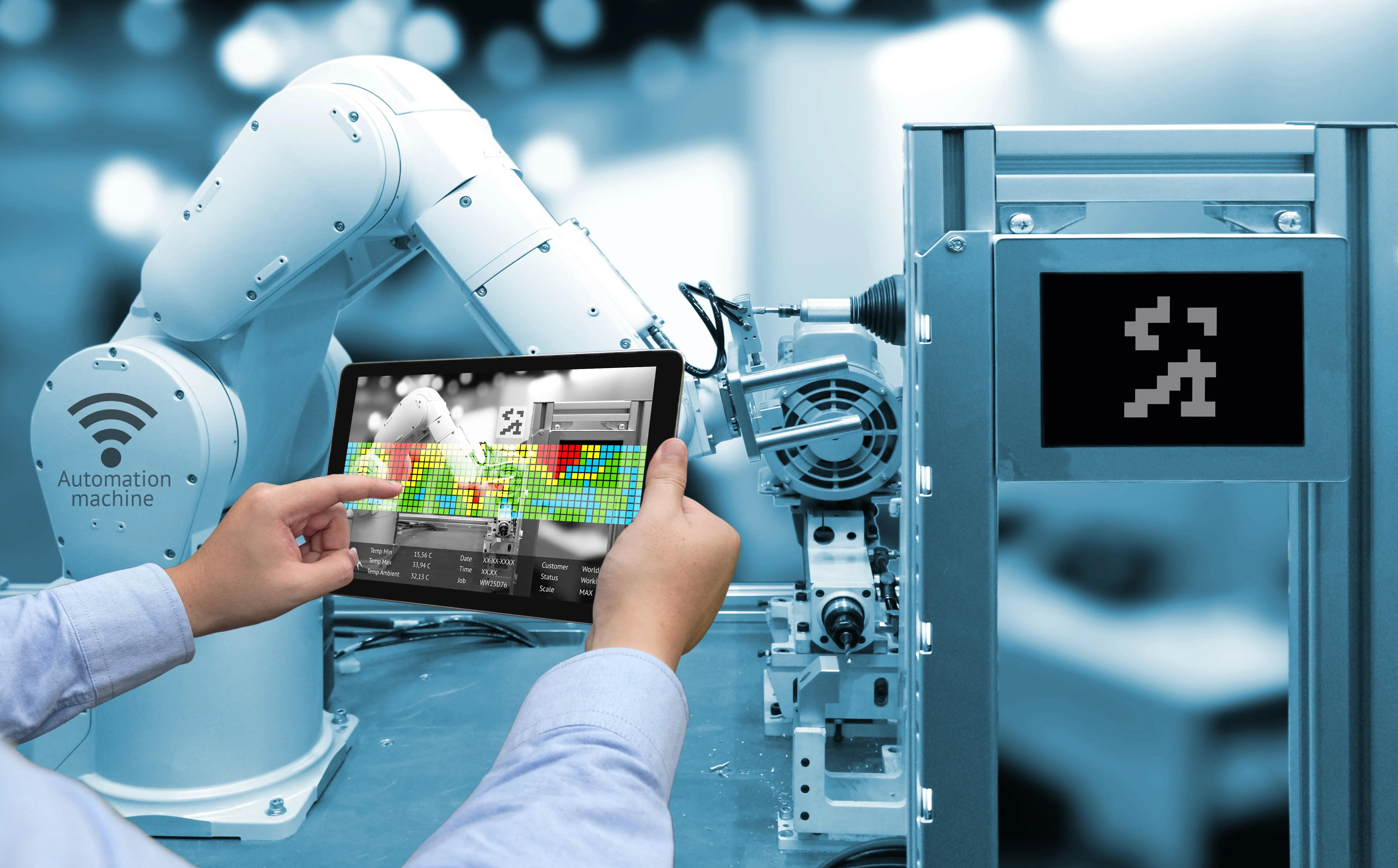
Part 2 of this two-part piece examines the potential benefits to be realized by pairing human Subject Matter Experts with smart silicon assistants, and what these new arrangements mean for semiconductor device manufacturing. Part 1 explores best-practice perspectives on collecting and utilizing smart data in industries outside semiconductor manufacturing, one of the important takeaways from the Smart Manufacturing panel discussion at SEMI ASMC 2018. So what does this observation (i.e. the field of medicine, in what seems at first glance a big data environment, is really just clusters and clusters of loose small data connected by the collective neural network of highly trained doctors and their colleagues) mean for semiconductor manufacturing? We think it means we need to apply the same level of intense focus that we already devote to instrumented data collection and analytics in the fab to something more: we need to better capture the vast expertise of our engineering and operational talent in semiconductor manufacturing. We think we need to record what the subject matter experts (SMEs) in the fab see, hear, and think as they investigate yield excursions or machine-down problems. We need to effectively combine product, process, equipment and component subject matter expertise / subject matter experts (SME) with big data analytics to more effectively solve manufacturing problems, be they killer or be they chronic. And we must provide structured methods for incorporating inputs from and active participation of SMEs throughout the data analysis lifecycle, from collection and aggregation, through filtering, feature extraction, analysis and optimization. Some of the challenge will be in just how do we make it easy to gather information from SMEs in real time, while standing in front of equipment in the fab. Internet of Things (Iot) devices are emerging to capture and label images and sounds to enable machine learning algorithms to recognize and help diagnose manufacturing problems based on sight and sound, complementing the instrumented data. But we also need to record the thought processes our human SMEs go through in those investigations – perhaps by the SMEs talking to a smart AI-based conversational assistant who helps make “rounds.” Doing contextual analysis on this added data, combined with the instrumented data, will create the equation Human + Machine = AI (Awesome Insight). Sounds reasonable, right? We think artificial intelligence becomes too artificial if you leave the human out of the equation. AI should be augmented intelligence, where we take the expertise and creativity of the human, and combine it with the rapid computational capabilities of the computer, in order to put problem identification and solutions on steroids. But with the already huge advancements to date in data analytics, cloud, and the emergence of AI, why do improvements in quality, machine utilization, and the implementation of predictive analytics in semiconductor manufacturing seem to be creeping along incrementally, and not appearing as dramatic, step-function improvements? Call it Smart Manufacturing, call it Connected Enterprise, call it Advanced Manufacturing, or Analytics, or Cloud, or the Digital Twin … there are no shortages of terms, philosophies, and technologies available, but why aren’t we seeing their rapid adoption? It could be it’s the downside that comes with needing people. “Good business leaders create a vision, articulate the vision, passionately own the vision, and relentlessly drive it to completion.” Jack Welch. We see from other industries that smart manufacturing conversations originating with the executives of a company thinking to implement smart manufacturing programs lead to vision; however, we also see from other industries, and from our own, that realizing this vision has often been a challenge. Why is that? One reason may be that the people who are personally vested in solutions they implemented in the past, as well as those who follow a pattern of ‘how we’ve always done things’, create, inadvertently or not, persistent internal barriers hindering innovative action. Another may be that engagements with the working engineers and managers charged to be smart manufacturing implementers leads to the pursuit of low-hanging fruit, and cautious investments, that often utilize solutions that ultimately cannot scale and integrate. Not to mention the disadvantage of dealing with the legacy equipment, the legacy networks, the traditional thinking, and the lack of consistency in metrics adding to the confusion. Addressing all these barriers requires an alignment in strategy and execution, along with a plan to support the overall vision, often across the entire enterprise, which is no small matter. And then there are the standards. Having and adhering to standards in control solutions, networks, and data becomes critical in achieving real benefits from smart manufacturing. And data security. One of the other big impediments in the smart manufacturing transformation is data and IP security, another key concern (maybe the most significant) preventing us from moving forward more quickly (e.g. to cloud-based solutions) in our industry. More about that in a follow-up. Achieving synergy across all of manufacturing, from connecting equipment horizontally, through the production system (machines processes), and vertically, through enterprise systems and across production facilities, can only occur if we build standards, security, infrastructure, and human engagement throughout our ecosystem and supply chain. In simple form, the steps to do so include connecting assets, collecting and contextualizing data, and then driving business transformation with actionable insights gained from the data. With impact on every function, and every person, in the enterprise, from equipment operators in the fab through the C-Suite in HQ. Maintenance, Engineering, R D, Operations, Scheduling, IT, Procurement, Finance, HR all contribute, collaborate and benefit. Regardless of the technology, from device level analytics to predictive maintenance and optimization, the people that reside in these disparate groups need to come together with the smart machines to create a common strategy to achieve transformational results. Aligning an enterprise’s goals with its human capital is paramount to success. Therefore, we must challenge our team members and ourselves to work outside our comfort zones, and we need to be forever aware of the need for us to grow with the technology. Smart manufacturing is not necessarily about having fewer people in the fab, but it does suggest having people in the fab, perhaps with different, or upgraded, skill sets, who are even more efficient in their roles as a result of the boost they are getting from Industry 4.0. Fortunately, we now have techniques that let us combine the best, brightest, and latest and greatest analytics with our invaluable SMEs throughout the data analysis lifecycle. We’ll not only be able to deliver higher quality semiconductor manufacturing solutions all in all, but we’ll also be providing methods to more easily distribute, scale, maintain, and continually refine those hard-earned solutions. We expect that subject matter experts will continue to put the “smart” in machine-based smart manufacturing today, and for the foreseeable future. SME contributions are not an option, but, rather, an imperative for ensuring a semiconductor manufacturer’s sustained prosperity, much less its survival. Nancy Greco (IBM Watson), Dave Mayewski (Rockwell Automation), James Moyne (University of Michigan / Applied Materials), and Paul Werbaneth (Intevac, Inc.), along with Julie Jacob (Ernst Young), and Carson Henry (Micron Technology), were members of the SEMI ASMC 2018 panel discussing Industry 4.0 and the Future of Commercial Semiconductor Device Manufacturing. All opinions here are purely our own. Please contact Paul Werbaneth via email at [email protected]. The SEMICON West (July 9-11, 2018, in San Francisco) Smart Manufacturing Pavilion features working production equipment on the floor and three full days of speakers providing insights on building the infrastructure needed to enable AI. Equipment from Bosch Rexroth, Cimetrix, Rudolph Technologies, INFICON, Final Phase Systems, OMRON, DISCO and Edwards Vacuum will showcase cutting-edge smart manufacturing technologies. For information on the SEMI Smart Manufacturing initiative and how to get involved, please click here.
Read More
Part 1 of this two-part piece explores best-practice perspectives on collecting and utilizing smart data in industries outside semiconductor manufacturing, one of the important takeaways from the Smart Manufacturing panel discussion at SEMI ASMC 2018. Part 2 examines the potential benefits to be realized by pairing human Subject Matter Experts with smart silicon assistants, and what these new arrangements mean for semiconductor device manufacturing. The spacecraft Discovery and its HAL 9000 computer system had a digital twin. Did you know? Stanley Kubrick’s seminal film “2001: A Space Odyssey” had its theatrical release 50 years ago this April. “2001” isn’t just a great science fiction film. Rather, it’s a great work of cinema overall, across any category. (The American Film Institute lists “2001” as #15 in the AFI Top 100; a bit below “Vertigo,” a bit above “It’s A Wonderful Life.”) It’s a film so distinguished and so prescient that its lessons can inform our thinking about smart manufacturing, Industry 4.0, and artificial intelligence (AI) today. Not to give too much away, but the earth-bound digital twin of Discovery / HAL identifies a diagnostic error the onboard, Jupiter-bound HAL 9000 has made, things go awry from there, and one of the mission pilots, astronaut Dave Bowman, is forced to intervene. At the recent SEMI Advanced Semiconductor Manufacturing Conference, ASMC 2018, on 02 May 2018 in Saratoga Springs, NY, five diverse panelists representing capital equipment, IDMs, academia, the semiconductor supply chain, and smart manufacturing best practices outside the semiconductor industry engaged in a lively discussion with the ASMC attendees. They explored where “smart” is in our industry today, where it’s headed, and what that’s going to mean for us -- the professionals who have brought semiconductor manufacturing to the current state of smart, and are looking to implement an ever-smarter tomorrow. Not to give too much away, but the panelists and audience agreed that there’s nothing artificial about pairing human intelligence with machine-based smart manufacturing. Implementing an ever-smarter tomorrow in semiconductor manufacturing requires smart people just as much as it requires smart machines. Moving towards “smart” means understanding how to derive useful information and actionable intelligence from the ever-increasing pool of big data created during semiconductor manufacturing. Modern manufacturing sites are extensively instrumented today, and create massive amounts of data to consume, decipher, base decisions upon, or discard. As we dig into this problem we realize that equipment and processes in our industry are both obviously complex, but, also, subtly complex. Semiconductor manufacturing tools easily contain 100s to 1000s of components working together to produce nanometer scale, angstrom scale, or even atomic scale features using complex chemical, physical, and plasma processes. There is a plethora of potential failure points and modes, and despite our best efforts to collect more data, many processes continue to be only poorly observable. On top of that, semiconductor fabrication processes are always drifting, and the operational context is continually changing as we change product mix, process maintenance swap-out kit components, and operating conditions and recipes. Sounds like … hospitals, and healthcare? When you see your doctor, she will collect and look at your instrumented data – blood work, blood pressure, weight, and other quantifiable factors. But, typically, your doctor won’t draw a conclusion based on that analysis alone. Rather, your doctor will sit with you, ask probing questions, and record what she asked, your responses, and what she saw, what she heard, and what she thought. Then she’ll build a hypothesis, combining the “anecdotal” data with the instrumented data, and derive from that data set both a likely diagnosis and an effective course of action. In this case, beyond the instrumented data, two humans, and their natural language input, are part of the equation: the patient, with his observations and thoughts, as well as the doctor, with hers. And it’s been a formula for success. Healthcare has made huge, step-function improvements across a spectrum of deadly diseases, as well as with less-deadly chronic afflictions, by harvesting this complex input, committing the proven disease presentation – disease diagnosis – and disease treatment models to medicine’s collective memory, and then teaching the next generation of healthcare providers both the general methods and the standard protocols essential to maintaining good health and successful outcomes. Maybe, in medicine, what seems a big data environment is really just clusters and clusters of loose small data connected by the collective neural network of highly trained doctors and their colleagues. Nancy Greco (IBM Watson), Dave Mayewski (Rockwell Automation), James Moyne (University of Michigan / Applied Materials), and Paul Werbaneth (Intevac, Inc.), along with Julie Jacob (Ernst Young), and Carson Henry (Micron Technology), were members of the SEMI ASMC 2018 panel discussing Industry 4.0 and the Future of Commercial Semiconductor Device Manufacturing. All opinions here are purely our own. Please contact Paul Werbaneth via email at [email protected]. The SEMICON West (July 9-11, 2018, in San Francisco) Smart Manufacturing Pavilion features working production equipment on the floor and three full days of speakers providing insights on building the infrastructure needed to enable AI. Equipment from Bosch Rexroth, Cimetrix, Rudolph Technologies, INFICON, Final Phase Systems, OMRON, DISCO and Edwards Vacuum will showcase cutting-edge smart manufacturing technologies. For information on the SEMI Smart Manufacturing initiative and how to get involved, please click here.

Read More
Emboldened by advances in self-driving and Internet of Vehicles (IoV) technologies, Taiwan’s microelectronics sector is investing heavily in manufacturing processes and equipment as engines of innovation and growth for autonomous driving, the world’s next market goldmine. But breaking into the self-driving vehicle industry can be a steep uphill climb. Semiconductor players hungry to secure their piece of the potentially massive market must know how to navigate the automotive industry’s unique ecosystem of suppliers, not to mention its lofty standards for safety and reliability.To explore opportunities and challenges in the automotive semiconductor market, SEMI recently organized Mobility Tech Talk – a gathering of experts from Strategy Analysis, Yole Développement, Renesas, X-FAB and IHS Markit who examined the evolution of sensors for autonomous cars, advanced driver-assisted system (ADAS) applications, and new energy vehicles (NEVs) in China. Nearly 200 participants exchanged in-depth, forward-looking insights and perspectives as the event helped forge stronger relations among various market segments. Here are four key takeaways from the conference. Lidar: The Hottest Sensing Technology for Smart AutomotiveLidar, mmWave radar, cameras and inertial measurement units (IMUs) are critical sensing devices for autonomous cars. With sensor and high-speed computing technologies maturing at their current pace, some 350,000 self-driving vehicles are expected to hit the road by 2027. But before a single autonomous vehicle takes to the roadways, self-driving technology must become expert at monitoring a vehicle’s environment.That’s where Lidar, the hottest of all sensing technologies and the key to the holy grail of safe self-driving, comes into the picture. Lidar’s versatility supports multiple essential functions such as mapping, object detection and object movement. The problem is that mass production is still impossible due to the technology's high costs. What’s more, technical issues must still be sorted out with solid-state lidar, mechanical lidar and MEMS. Both startups and traditional tier-1 semiconductor manufacturers are aggressively investing in related research and development in hopes of fulfilling lidar's promise and seizing the market opportunity. Smart Automotive Sets New Quality and Safety StandardsAs cars become smarter, so too must silicon. Chips must support vastly more data generated by in-vehicle connectivity, ADAS, electrification, autonomous driving and an array of other functions that rely on advanced automotive electronics components. With demand for smarter silicon surging, Taiwan semiconductor companies are turning to the automotive chip industry for expertise and serving as OEMs for major automakers.Quality and safety for automotive applications is paramount. In-vehicle semiconductors must meet strict requirements for vehicle control, robustness, liability, cost and quality management to meet the automotive specifications necessary to securing certifications. Smart silicon must also pass all AEC-Q liability standards promoted by North America automakers and score “zero defect” for the ISO/TS 16949 Automotive Quality Management System.China’s New Energy Vehicles To Fuel Semiconductor GrowthTo promote NEVs and reduce fuel consumption of cars with internal combustion engines (ICEs), late last year the Chinese government introduced the Measures for the Parallel Administration of the Average Fuel Consumption and New Energy Vehicle Credits of Passenger Vehicle Enterprises. With China the world’s largest market for NEVs, the policy is forcing automakers in Japan, the U.S. and Europe to accelerate moves towards NEVs that, in turn, will fuel growth in the semiconductor and automotive battery industries. NEVs in China are expected to number 2 million by 2020 before more than doubling to 4.9 million by 2025. Today, most cars still run on ICEs as environmentally friendly motor drives are still under development. In unit shipments, motor drives are expected to surpass ICEs by 2025.Cross-field Collaboration is KeyThe rise of smarter, fully autonomous vehicles – a disruptive Car 2.0 – is unlikely to happen overnight. Rapid growth of the global automotive semiconductor market will continue, with safety and powertrain applications driving the strongest chip demand. Meanwhile, automakers are focusing more on innovations from startups and non-traditional suppliers, and some have even started to develop their own IP and solutions. These paradigm industry shifts are diversifying the automotive supply chain into a cross-domain collaborative network of suppliers, pushing the closed, one-way automotive supply chain into lesser relevance. In the near future, rivals and partners may become indistinguishable as traditional turf wars begin to wane. As ADAS and autonomous cars evolve, and the era of electric cars nears, automotive semiconductors are emerging as the engine of growth for the global semiconductor industry. The automotive semiconductor market is expected to grow at a CAGR of 5.8 percent, reaching US$48.78 billion by 2022.For its part, the SEMI Smart Automotive special interest group connects professionals from the microelectronics and automotive industries. The group promotes the semiconductor industry's development of automotive technologies and cross-domain collaboration to help drive autonomous vehicle innovation.
Read More