downloadGroupGroupnoun_press release_995423_000000 copyGroupnoun_Feed_96767_000000Group 19noun_pictures_1817522_000000Member company iconResource item iconStore item iconGroup 19Group 19noun_Photo_2085192_000000 Copynoun_presentation_2096081_000000Group 19Group Copy 7noun_webinar_692730_000000Path
Skip to main content
Default Banner Image

microelectronics

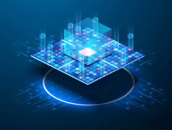
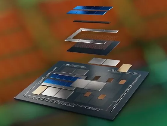
Throughout the current millennium, System-on-Chip (SoC) has been the gold standard for optimizing performance and cost of complete electronic systems. By incorporating practically all the phone’s digital plus analog capabilities onto a single, giant chip, the mobile phone processor serves as a near-perfect exemplar of SoC. But today’s leading integrated circuits (IC) are pushing up against the upper limit of a chip’s size which is limited by the manufacturing equipment’s optical reticle size. This has proven difficult to increase and has grown only slowly over the years. Yet market pressure continues unabated for bigger, more capable electronic systems with more integrated memory, more digital logic, and more analog/mixed signal circuitry. An emerging solution to this tension is 3D and 2.5D multi-die chip assemblies – often referred to as 3D-IC. The key technology breakthrough of 3D-IC is that it makes it possible to spread a system out over multiple, smaller chips that are then assembled close together and interconnected with high-speed, low-power interconnect technologies. By abandoning the need to integrate an entire system on a single SoC and instead allowing it to be disaggregated over multiple chips, 3D-IC enables Moore’s Law to break through the reticle size barrier, improves yield by shrinking the size of individual chips, and makes it possible to mix different process technologies optimized for each function. The Four Engines Driving Semiconductor Design The road forward is not without its challenges, however, and we are seeing design companies making significant efforts to adapt and come to grips with the following four technology and market drivers: The requirement for concurrent multiphysics analysis to ensure reliable and efficient electronic systems The blurring of the lines between silicon and system The need for open and inclusive multiphysics platforms that interoperate with the multitude of design platforms The need for, and value of, bespoke silicon for hyperscalers and system companies Blurring of Silicon and System Design The advent of 3D-IC opens up new horizons for solutions that can be implemented in silicon. But it also forces a closer integration between two distinct technology markets that have co-existed symbiotically for many decades: IC design and printed circuit board (PCB) design. These markets use different tools, different data formats, different manufacturing back-ends, operate at different computational and geometric scales, and focus on different physical concerns. Yet, 3D-ICs share many aspects of both markets: They include monolithic chips but also board-like substrates to stitch the chips together. And in between the two disciplines is packaging, a completely different domain that is requiring companies to re-imagine their design capabilities and flows, as well as their organizational structure. Open, Extensible Multiphysics Platforms The siloed isolation of chip design from PCB design and package design means that each of these markets has developed insular data structures that are ill-suited to deal with the breadth of multiphysics analysis for 3D-IC design. Many different physical disciplines, including computational fluid dynamics, mechanical stress, and electromagnetic radiation, all need to work together based on open and extensible multiphysics platforms. These platforms must embrace the modern cloud compute paradigm and enable an ecosystem by allowing individual design platforms to connect for comprehensive multiphysics analysis. Bespoke Chips Today’s market-leading companies are heavily dependent on technology for their continued success and market differentiation. Everybody from online retailers to telecommunications to social networking companies and hyperscalers are moving away from off-the-shelf solutions and turning to custom-built silicon to give them an edge. Many of these companies are seeking to gain market share by leveraging proprietary AI/ML algorithms trained on their extensive troves of market data – but this requires huge amounts of compute power and specialized chips. Access to high-quality silicon solutions is vital in today’s world and the demand is for continually more complex and powerful electronics. 3D-IC an Inflection Point in Electronic Design To be sure, 3D-IC design is at an inflection point in electronic design and presents major challenges that are realigning the electronic design industry around this new reality. For more insights on this topic from a semiconductor industry leader, please view the Keynote Address 2.5D and 3D – The Road Ahead by Vicki Mitchell, VP Engineering, Arm Central Engineering Systems Group presented at the latest Ansys IDEAS Forum. And for an EDA perspective, please view Successful 2.5D and 3D Multi-die Silicon System Design Using Synopsys’ 3DIC Compiler and Ansys’ Multiphysics Analysis from Synopsys SNUG World 2021. About John Lee John Lee is general manager and vice president of the Ansys Electronics and Semiconductor Business Unit. Lee co-founded and served as CEO of Gear Design Solutions (now Ansys), developer of the first purpose-built big data platform for integrated circuit design. He cofounded two other startups (Mojave Design and Performance Signal Integrity), which successfully exited into companies now part of Synopsys. He holds undergraduate and graduate degrees from Carnegie Mellon University.
Read More
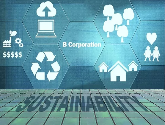
Becoming a Certified B Corporation™ comes with many benefits, most of them extending beyond the walls of the company and into the hands of employees, community members, and industry partners. The designation makes the meticulous and rigorous process to certification well worth the endeavor. In 2021, Brewer Science announced that it’s the first company in the semiconductor industry to become a Certified B Corporation. Our journey to become a Certified B Corporation inspired us to share our top five reasons for meeting the high standards the designation sets for both environmental and social responsibility. 1. Pave a pathway for continuous improvement B Lab™, the certifying organization for B Corps, believes in continuous improvement, and B Corps must create an improvement plan to demonstrate the areas of social and environmental performance they focus on in the coming years. Brewer Science will hold B Corp certification for three years before submitting to a renewal process. In order to be recertified, a company must score higher on recertification than on the previous certification. The assessment evaluates all facets of the company, and it’s a learning process to help the company target and identify ways to improve business practices. Brewer Science has already identified improvement areas for the recertification. We’ve implemented several human resource initiatives that are not written into policy yet, such as flexible and expanded work options. Additionally, we have expanded our use of a cloud-based learning platform to provide employees with more training options and performance conversations held quarterly instead of annually. Brewer Science scored many points for community involvement and charitable giving. However, we are still expanding community engagement by supporting or donating to a new local organization each month. Brewer Science became Certified Employee-Owned in 2020, but since it was the first year of the ESOP and shares were not yet dispersed, B Lab didn’t fully recognize the program. 2. Share the values of your stakeholders In 2006, Brewer Science started externally reporting environmental, safety, and health performance every year through its annual Corporate Sustainability Report in order to be transparent with customers, suppliers, and employees. The impact of this report on all of our stakeholders motivated us to pursue other ways to promote sustainability and inclusion as a shared asset for our customers and suppliers. In 2016, Brewer Science became GreenCircle Certified Zero Waste to Landfill, an annual certification that we have achieved every year since then. Certified B Corporations are businesses that meet the highest standards of verified social and environmental performance, public transparency, and legal accountability to balance profit and purpose. The standard is highly respected standard, in part because of B Lab’s rigor with the questionnaire and certification process. Not only does becoming a B Corp show your stakeholders that you care, and that you are walking the walk, but it also allows you to show how much your company cares through your B Corp Impact Area. Brewer Science pursued the impact area of environmentally innovative manufacturing, a category that required detailed evidence of how Brewer Science manages the manufacturing waste and minimizes its carbon footprint. The B Impact Area Scores reflect the five areas where the business excels. 3. Be competitive in an industry that demands sustainability and social responsibility Sustainability is of growing importance in the semiconductor industry. A company can convey its commitment to sustainability by becoming a Certified B Corp. The B Impact Assessment requires benchmarking to other companies in the industry in areas of social concern, such as sustainability, inclusion, and diversity. While benchmarking was nearly impossible for Brewer Science since we rank high as an innovator in these areas, we were able to not only set the benchmark for ourselves, but other industry partners who pursue B Corp certification in the future through our collaboration with B Lab. 4. Connect with a community that cares Becoming a Certified B Corporation instantly opens companies up to a network of other B Corps across the world. The more than 4,000 B Corps in 150 industries and 74 countries enables makes it easy to network in the areas such as environmental initiatives, attracting top talent, and even just using business as a force for good in the semiconductor industry. Knowing that a business is actively trying to make a positive social change will help attract top talent looking to find meaning in their careers. B Corp certification validates a company’s employee-centric culture, which can help beef up employee retention. What’s more, an exclusive job posting board called B Work, sponsored in part by B Lab, helps connect job seekers with companies that share their values. Employees are connected through an exclusive B Corporation community platform, B Hive, enabling them to collaborate and share ideas with other B Corp employees. There is also a section within the B Hive where other B Corps can share benefits with other B Corp member employees. With such a diverse range of companies that are Certified B Corps, shared benefits can include anything from discounted clothing to travel deals or even free consultations. Additionally, employees of B Corporations can collaborate on local recycling events and community engagement. 5. The bottom line Companies don’t pursue the Certified B Corp designation to drive improvements to their bottom line. Yet by sharpening their focus on environmentally sustainable initiatives and diversity and inclusion, most companies could indirectly see significant return on investment. For example, having a pathway for continuous improvement, sharing the values of your stakeholders, being competitive in the industry, and connecting to clientele and employees that value social responsibility all enable your business to grow. In the long run, becoming certified as a B Corp can save a company money by giving companies access to community data that provides insights into cost-effective ways to be more sustainable. Plus, the certification process helps companies identify wasteful spending. For more information about Certified B Corporations, and to get started on your company's application, visit the Certified B Corporation website. Jessica Albright is a content marketer at Brewer Science, Inc.
Read More
As monolithic scaling slows down, the semiconductor industry is increasingly relying on advanced packaging technologies to extend Moore’s law through heterogeneous integration. Higher on-package bandwidth, improved yield resiliency and the need to integrate diverse IP from multiple foundries are driving demand for advanced packaging technologies that address these issues but introduce challenges of their own such as efficient power delivery to all the different domains in a heterogeneous system. SEMI spoke with Kaladhar Radhakrishnan, Intel Fellow at Intel, about heterogeneous system integration trends and new developments in the semiconductor industry. Radhakrishnan shared his views ahead of his keynote at the SEMI Connecting Heterogeneous Systems Summit, 1-3 September 2021, an online event. Join the summit to meet experts from Intel and other key industry influencers. Registration is open. SEMI: What is driving the adoption of electronics and semiconductor devices nowadays and why is the development of new and innovative technologies important? Radhakrishnan: We are living in an increasingly data-driven world where devices have become an integral part of our lives. A recent study estimated that in the United States alone, 13.6 connected devices per capita consume an average of 300 gigabytes worth of data every month. In the workplace, COVID-19 has driven fundamental business changes that has sped up the adoption of digital technologies such as virtual conferencing, remote work, and e-commerce. Organizations are realizing that a high-quality video conference can be an adequate substitute for many in-person meetings. As a result, businesses are accelerating the digital transformation in order to adapt and thrive in this new environment. Five decades of sustained exponential growth in semiconductor performance has conditioned the average digital consumer to expect more from their devices. However, there are some headwinds ahead as traditional scaling slows down and power density rises. Because consumers and businesses are now generating data at a faster rate than they can consume it, technologists need to scale compute, storage, and bandwidth even faster to keep pace. Without investments in research and development of new and innovative technologies to address these challenges, the full potential of this data will go unrealized. SEMI: What forces are heightening the importance of heterogeneous system integration? What are the implications for increased on-package bandwidth, improved yield resiliency and the need to integrate diverse IP from multiple foundries? Radhakrishnan: The semiconductor industry increased transistor density and scaled performance through classical Dennard scaling until the turn of the century. By then, the gate oxide thickness had scaled down to atomic dimensions and the exponential increase in sub-threshold leakage signaled the end of scaling through traditional methods. Since that time, the chip industry has been relying on innovations in transistor materials and structures such as high-k metal gate, strained silicon, and FinFETs to keep pace with Moore’s law. However, this alone will not be sufficient to continue scaling and the industry needs to explore other vectors to augment improvements in transistor technology. Heterogeneous integration through advanced packaging is one key technology that can help drive these gains. Technologies like Foveros can enable device density scaling by creating a 3D stack of multiple die using high-density interconnects. Heterogeneous integration enables chipmakers to move from a monolithic system designed on a single large chip to a heterogeneous system comprised of a number of smaller chiplets. The main benefit of using smaller chiplets is that they improve yield and enable application based customization of the foundry processes. However, if the disaggregation to smaller chiplets is not accompanied by an increase in on-package bandwidth, the power and performance penalties associated with chiplet-to-chiplet communication will hobble system performance. This is why advanced packaging technologies that improve die-to-die communication are key enablers for heterogeneous integration. SEMI: What are some of the key technology challenges in developing heterogeneous systems? Radhakrishnan: The obvious challenge that most people focus on is the need for improved on-package bandwidth. However, as we rely on 3D stacking to continue device scaling at the package level, it is important to comprehend power delivery and thermal challenges as well. Power to the top die has to be delivered through TSVs on the bottom die, which not only adds resistance but also reduces the useful area available on the bottom die. This problem is further exacerbated when we stack more than two die. Excessive noise on the power delivery network can cause timing issues that limit the maximum operating frequency of the transistor. Similarly, when we stack multiple die, we must take into account associated thermal challenges. For example, each interface of the multi-die stack adds thermal resistance, which makes it harder to cool the chips at the bottom. SEMI: What are some of the key global market trends that driving demand for heterogeneous and system-level integration? Radhakrishnan: The number of artificial intelligence (AI) and machine learning applications have grown dramatically due to their ability to solve highly complex problems across a wide range of segments. AI and machine learning models require more memory bandwidth and compute capabilities that are difficult to achieve without some form of heterogeneous integration. Another market trend driving demand for heterogeneous integration is the increasing reliance on custom hardware accelerators. To combat the slowdown in frequency scaling and single-core performance, we have moved to multi-core architectures by tackling the inherent parallelism in our workloads. However, Amdahl’s law tells us that such an approach will hit a bottleneck when we reach the limits of the serial portion of the workload. As these constraints slow the performance of general-purpose processors, the reliance on custom hardware accelerators to boost performance for specific workloads is growing. Heterogeneous integration at the system level with a combination of CPUs, GPUs, FPGAs and other accelerators can optimize system power and performance. SEMI: What solutions is Intel developing to address these market needs? Radhakrishnan: Intel is actively involved in the development of the industry ecosystem for heterogeneous integration. We have developed a number of innovative advanced packaging solutions such as the EMIB and Foveros that are used in products today. Intel is also developing the next generation of advanced packaging technologies, Foveros Omni and Foveros Direct, which will dramatically scale the IO density by using direct Cu-Cu bonding technology. Foveros Omni is a crucial building block technology to enable high-voltage power conversion on the package for efficient power delivery. Intel is uniquely positioned to predict the design needs for future systems and deploy its resources to develop the technology building blocks needed to continue performance scaling. Our IDM 2.0 strategy enables us to leverage our leadership in packaging technologies to design the best products and use the best IP to deliver leading products across a broad range of categories. SEMI: What do you expect from your participation at SEMI Connecting Heterogeneous Systems Summit? Radhakrishnan: I’m hoping to shed some light on some of the new technologies we have been developing at Intel to enable heterogeneous system integration. I also want to bring awareness to the power-related challenges we are facing with heterogeneous systems. I also look forward to listening to what other industry leaders have to say on the topic. Kaladhar Radhakrishnan is an Intel Fellow and a Power Delivery Architect with the Technology Development group at Intel. He plays a significant role in shaping and driving power delivery technologies for Intel microprocessors. His areas of expertise include integrated voltage regulators, advanced packaging and passives technologies. Kaladhar is a two-time recipient of the Intel Achievement Award, the highest Intel honor an individual or small team can receive. He has authored four book chapters, over 40 technical papers in peer-reviewed journals, and has been awarded 35 U.S. patents. He has also served as an adjunct professor at Arizona State University. Kaladhar joined Intel in 2000 soon after receiving his Ph.D. in Electrical Engineering from the University of Illinois at Urbana-Champaign. Serena Brischetto is senior manager of marketing and communications at SEMI Europe.
Read More
Taking aim at advancing smart medtech innovation, the SEMI Nano-Bio Materials Consortium (NBMC), in collaboration with the U.S. Air Force Research Laboratory (AFRL), in March 2020 identified 12 organizations from industry and academia as recipients of $20.4 million in funding, leveraging $10.7 million of cost-share from award recipients. Unique to this round – the sixth in NBMC’s eight years – is a pilot program for NBMC and AFRL to collaborate more closely and share more resources. As part of that effort, AFRL is contributing additional funding to seven of the 12 projects to enable its researchers to work alongside industry on the projects in the new AFRL-Industry Co-Development Program. After being matched to a project during pre-RFP discussions – also known as the White Paper Stage – AFRL researchers were designated as NBMC Consortium Project Investigators before collaborating with industry on the second stage of proposal development. Once contract negotiations between NBMC and the proposing entity wrap up, the AFRL investigators will participate in the development of smart medtech innovations. “This is a new way for AFRL researchers to participate as project performers responsible for contributing to project milestones and deliverables, in addition to providing program management oversight that AFRL has employed for past NBMC projects,” said Dr. Jeremy Ward, past NBMC government lead and current participant in the AFRL Entrepreneurial Opportunity Program. “This program should enable technical risk-reduction for industry by leveraging AFRL competencies and U.S. Air Force aeromedical and airmen performance mission connectedness and ultimately help speed the development of dual-use smart medtech,” added Matt Dalton, AFRL Materials and Manufacturing Directorate program manager and NBMC Governing Council member. “We need efficient mechanisms to leverage research being done outside of AFRL,” said Sharma, who is also senior technical lead for Cognitive Neuroscience at AFRL's 711th Human Performance Wing. “If someone is developing a groundbreaking technology that can be helpful for our airmen, then let’s work with them so that we have an opportunity at an early stage to actively shape that research for Air Force-relevant use cases. Similarly, with this co-development initiative, external researchers will also get an opportunity to work alongside world-class researchers at AFRL and, through those interactions, get insights into the needs of the operational community.” “The AFRL-Industry Co-Development Program strengthens the work between AFRL and industry to better target the strategic needs of the Air Force for dual-use technologies while more closely aligning with commercial market requirements,” said Dr. Melissa Grupen-Shemansky, SEMI CTO and Executive Director of NBMC. “This new collaboration will enable the growth of the ecosystem critical to bringing the latest smart medtech innovations to market while making the technology’s supply chain more sustainable and resilient.” SEMI NBMC connects military, industry and academia for research and development into the practical use of nano-biomaterials. The 2020 RFP targeted nano-bio materials for wearables, flexible and alternative power sources for wearables, and open concepts for wearables for diagnostics and ambulatory monitoring. These technologies address the critical need to monitor, evaluate and mitigate stress experienced by workers in high-pressure occupations – such as aviation, emergency, critical care and aeromedical evacuation – to enhance their warfighter performance and help ensure their well-being. For more information on SEMI NBMC, our R D funding projects, and how you can help shape the direction of our funding programs, visit our website or contact me at [email protected]. Learn more about our projects at the 2021 Global Smart MedTech Symposium July 28-29 and August 4-5, 2021. For more information about the NBMC-AFRL collaboration, see the 2020 Smart MedTech Virtual Workshop agenda. This article borrows from a U.S. Air Force press release on May 27, 2021. Rene Krantz is program manager for SEMI NBMC Smart MedTech.
Read More
As the global economy is constantly transformed, the need for new skills has never been higher. The microelectronics industry is thoroughly affected by this urgent need. To develop a workforce fit for the future, it is crucial to invest not only in reskilling and upskilling, but also in skills anticipation and inclusivity. To tackle this need, the European microelectronics ecosystem has adopted many bottom-up initiatives and good practices supporting lifelong learning. Many companies collaborate with universities and training institutes to offer work-based training, and numerous events take place to support women participation in STEM and to attract more young talent to a microelectronics career. Despite these great efforts, further pooling of investments is necessary if Europe is to develop efficient lifelong learning programs. Creating strong skills partnerships is vital for sustainable upskilling and reskilling initiatives. According to the World Economic Forum (2021), greater private-public collaboration on large-scale upskilling and reskilling initiatives could boost global GDP by $6.5 trillion and lead to the creation of 5.3 million net new jobs by 2030. What is the Skills Partnership? Against this backdrop, SEMI Europe is launching the Skills Partnership for Microelectronics. The partnership brings together industrial and education partners from the microelectronics ecosystem to implement the Pact for Skills, an EU initiative which aims to boost upskilling and reskilling investments in key ecosystems for Europe’s competitiveness. Following the high-level roundtable with SEMI Europe’s Advisory Board, hosted by European Commissioners Thierry Breton and Nicolas Schmit, the microelectronics sector was selected in November 2020 as one of the key ecosystems for the first wave of implementation of the Pact, alongside automotive and aerospace/defense. Read more details about the October 2020 roundtable. 59 partners have already endorsed the Pact for Skills for Microelectronics. The Skills Partnership for Microelectronics aims to: Exchange good practices of upskilling and reskilling initiatives of the microelectronics industry Develop sustainable collaboration mechanisms that will monitor microelectronics skill needs, learning from the examples of the METIS blueprint project Promote the microelectronics sector as a career choice Boost the presence of women and other under-represented groups in the sector. The partners will have the opportunity to liaise not only with European, but also with national and regional authorities and clusters, so that a pan-European holistic approach to microelectronics skills development is achieved, and a significant flux of public and private investments on skills is mobilized. To launch this ambitious partnership, SEMI Europe held an initial workshop on March 17. Participants included representatives from the European Commission’s DG Connect, DG Employment and DG Grow, national and regional authorities, and over 70 industry and education partners. The workshop opened with representatives from the European Commission informing all stakeholders about the Pact for Skills initiative, as well as about EU skills-related funding opportunities. In the framework of the Pact for Skills, the Commission will support the ecosystems with a Networking Hub, a Knowledge Hub and a Guidance Resources Hub. These platforms will be available later in 2021 and will act as a one-stop-shop to support the partners and provide information on EU policies and funding opportunities. Other presentations went on to set the scene, presenting the main priorities of the partnership. Françoise Chombar, CEO of Melexis, highlighted the skills challenge experienced by the microelectronics industry. She emphasized the importance of lifelong learning and the danger of the gender disbalance in the sector and underlined the huge innovation potential and profitability that could be unleashed for Europe if the gender gap is successfully addressed. Moreover, the preliminary results of the METIS Microelectronics Skills Strategy were presented, to offer the basis for the partnership’s approach to skills anticipation. The partnership will establish working groups that will investigate the industry needs, leading to a better connection with the offer of education and training programs. Last but not least, the partnership aims to promote national and regional funding of upskilling and reskilling initiatives. In this regard, representatives from national and regional authorities and clusters participated in the meeting. The government of the Basque region had an active role, presenting the region’s priorities, incentives and main actions on promotion of lifelong learning initiatives. The next steps The meeting concluded with an overview of the next steps for the newly launched partnership. In the next workshop, the partners will align on the specific KPIs, as well as on the focus areas where they would like to engage (skills anticipation in semiconductor manufacturing, skills anticipation in semiconductor design, gender balance, etc.). In that framework, the executive board will be established, as well as the working groups that will lead the work of the partnership and set targeted objectives. If you want to take active part in the creation of this large-scale initiative, please fill in your details here. To learn more about the initiative, click here or contact [email protected]. Stefania Gavra is public affairs manager at SEMI Europe.
Read More
MEMS actuators transform electronic signals into something that can be sensed or touched by the end user of an electronics device. A case in point: MEMS actuators such as print heads in inkjet printers transform electronic files into text or beautiful images. In 3D printers, actuators can produce real objects. Inside smart glasses, tiny MEMS mirrors can create virtual objects. Little surprise, then, that integrating these powerful devices into the end products is a multidisciplinary enterprise. STMicroelectronics has been successfully leading the deployment of dedicated MEMS actuator solutions with customer products in various market segments. SEMI spoke with Anton Hofmeister, group vice president and general manager of the MEMS Actuator Division at STMicroelectronics, about MEMS actuator trends. Hofmeister shared his views at the SEMI MEMS Imaging Sensors Forum as part of the virtual SEMI Technology Unites Global Summit. Watch the STMicroelectronics’ presentation on-demand until March 26, 2021. Registration is open. SEMI: What is the difference between MEMS devices that sense and MEMS devices that actuate? Hofmeister: MEMS sensors gather data from the world around us including motion, pressure and air temperature and transform them into an electrical signal. Actuators work the other way round. They receive an electrical signal and transform it into some well-controlled actuation such as ejecting a fluid, moving a membrane or deflecting a laser beam. SEMI: How can MEMS actuators’ integration be simplified to be embedded in new applications so they appeal to consumers? Hofmeister: The challenge of integrating MEMS sensors into devices has been simplified by demo kits and evaluation boards, which customers use to embed the sensor into a system. MEMS actuators are more difficult to integrate. They often power the core function of a system and therefore require deep system understanding. Reference designs are a big step forward in simplifying integration. My presentation at the SEMI MEMS Imaging Sensors Forum showcased some examples. MEMS micro-mirror projection for augmented reality (AR) glasses is an example of a complex system that requires multiple types of components to function. Together with several partners, STMicroelectronics recently announced the LaSAR Alliance, which will develop reference designs to enable the AR glasses market. SEMI: MEMS sensors and actuators are considered the backbone of many consumer products. Are MEMS actuators also mostly used in automotive? Hofmeister: The widest use of MEMS actuators has so far been in print heads for inkjet printers. In recent years, we have seen actuators adopted in emerging applications ranging from piezo heads for 3D printers to MEMS mirrors for laser beam scanning systems or 3D sensing solutions for consumer applications. The first high-volume application in automotive will likely be MEMS mirrors for LIDAR systems. SEMI: What market growth trends do you see for MEMS sensors and actuators? Hofmeister: The sensorization trend, which aims to collect data from homes, cities, factories, cars and personal devices, continues to drive the adoption of sensors and actuators for a wide variety of applications. While the last wave of MEMS growth was triggered by one end product – the smartphone – the next wave will be driven by multiple applications and use cases in industrial, medical, automotive and personal electronics. SEMI: How can technology unite us? Hofmeister: In recent months, we have all experienced vividly how vital technology has become. MEMS, and semiconductors in general, are an integral part of many products and services that make our lives easier. Communications technologies have been particularly important during this pandemic, whether using the personal devices as our interface to the digital world or the complex infrastructure that they operate through. I hope that my participation at the summit helped increase awareness of the new possibilities and opportunities that technologies like MEMS actuators have to offer to create products and services that further improve people’s lives. Anton Hofmeister is group vice president at STMicroelectronics, general manager of the company’s MEMS Actuator Division and managing director of its German subsidiaries. Hofmeister has been with STMicroelectronics for more than 30 years, working in Germany, France, the U.S. and Italy. He has held managerial positions in key account management, product and strategic marketing, advanced R D and general management. For the past 10 years, he has managed various product divisions in the MEMS sector. Hofmeister has also served as a board member of the Singapore-based molecular diagnostics company Veredus Laboratories. Serena Brischetto is senior manager of Marketing and Digital Engagement at SEMI Europe.
Read More
For the first time in its 20-year history, the FLEX Conference dedicated an entire session to the important and timely twin topics of environmental sustainability and power consumption of electronic devices. The event planning committee recognized the urgent need to increase the awareness of how technology and electronics devices can help reduce greenhouse gas emissions (GGE) overall and meet aggressive targets to curb the impacts of climate change. Dr. Christine Ho, CEO of Imprint Energy, delivered the keynote for the session, focusing on the need for powering billions of sensors that will be deployed annually, and their role in reducing fossil fuel emissions through becoming aware of issues, monitoring our resources over time, and intervening early and often to combat waste in multiple sectors and industry. Quoting extensively from the organization Exponential Roadmap Initiative (ERI), Ho noted that “the digital sector has the potential to directly reduce fossil fuel emissions 15% by 2030 and indirectly support a further reduction of 35% by influencing consumer and business decisions and systems transformation.” The initiative’s playbook for reaching net zero carbon emissions by 2050 and limiting global warming to 1.5° Celsius outlines how the digital sector can help remove 13 of the 27 gigatons (GT) of CO2 needed to reach this goal. Ho stated that the rapidly emerging Internet of Things (IoT), devices, software systems, and data insights are the backbone of this digital transformation. The IoT's vast network of sensors can transform multiple sectors, such as the logistics industry, which on an annual basis moves and ships more than 10 billion tons of products worldwide by ships, airplanes, long haul trucks, and train - contributing 17% of GGE and more than 4 gigatons of CO2 annually. Always-connected IoT sensors used by the logistics industry can reduce waste and damage in the supply chain, which is especially problematic for temperature-sensitive and damage prone pharmaceutical and food products, mitigating the need for producing high volumes of buffer inventory to replace damaged goods Noting that the attendees of 20 Years of FLEX Conferences were a big part of the current advancements of low-cost printed, active, shipping tags, Ho said that Imprint Energy’s flexible and thin, Zinc based batteries are ideal for IoT devices, since they boast a significantly smaller carbon footprint than Lithium-Ion (Li-ion) batteries. Imprint Energy is working with systems designers and integrators to design the battery as an integral part of the device package and use low-power strategies to extend device lifetimes. Imprint recommends co-locating battery printing alongside the device integration to further minimize shipping and logistics. When manufactured separately, Imprint’s small footprint, low-operating temperature process line (less than 80°C) provides significant carbon footprint advantages over other technologies. Ho challenged the attendees, saying “we all need to participate in protecting our earth. We need to eliminate waste and contribute to reducing half of our current greenhouse gas emissions by 2030, and we can do that by deploying a global digital skin with more than 100 billion IoT devices in 2030 and up to 1 trillion by 2050. We can minimize the device carbon footprint and maximize its longevity by considering the power capability, as well as design for re-use and re-cycling of the critical materials.” Following Dr. Ho’s presentation, FLEX kicked off a spirited panel discussion with experts from PowerRox, ITN Energy Systems, Birla Carbon, and Auburn University and chaired by Bob Praino and Eric Forsythe, from Chasm Advanced Materials and the Army Research Labs, respectively. The speakers summarized their on-demand presentations and looked at what is being done today to recycle Lithium-Ion batteries, how IoT devices are currently being powered, and drew comparisons between the early days of the Internet and development of the IoT. The speakers generally agreed that the power requirements of wireless cellular and Blue-tooth devices were still too high and run times too short. FLEX 2021 was a virtual event in the 2021 SEMI Technology Series. It was organized by SEMI FlexTech, SEMI NBMC, and NextFlex. Major sponsors included E Ink and Novacentrix. The event covered technical developments in flexible, printed and hybrid electronics, featuring more than 100 presentations and networking opportunities. Technical proceedings are available until March 26 at http://flex.semi.org. Heidi Hoffman is senior director in Corporate Marketing at SEMI.
Read More
With each transition to a new technology node, fab requirements for metal and particle contamination become more stringent, posing challenges for existing coating methods such as anodization or plasma spray that may not provide complete protection against contamination especially on critical chamber components with complex geometry. SEMI spoke with Beneq business executive Sami Sneck about common metal and particle contamination issues with critical chamber components, coating methods to protect against corrosion, and properties to look for when selecting the optimal protective coating solution. Sneck discussed the unique benefits of atomic layer deposition (ALD)anti-corrosion coatings with Aluminiumoxide (Al2O3) and Yttrium Oxide (Y2O3) and offered recommendations on how to work with original equipment manufacturer (OEM) partners to design, test and implement an ALD coating solution for semiconductor equipment. To learn more, visit Beneq at its digital booth at SEMI Technology Unites Global Summit, available on-demand until March 26, 2021. Registration is open. SEMI: How does ALD compare with other coating methods such as anodization and plasma spray? Sneck: ALD enables conformal dense and pinhole-free coatings on complex shapes. We can deposit various ALD coating materials on parts made of various materials. All other coating techniques have limitations. For instance, anodization is conformal, but porous and is suitable for Al2O3 used for aluminum parts. Plasma Spray is a line-of-sight method and not conformal on complex shapes, such as holes in showerhead parts. SEMI: Which substrate materials work for ALD coatings? Sneck: In general, parts made of common metal materials, such as aluminum, stainless steel or titanium, all work well with ALD coatings. Commonly used ceramic materials work well with ALD too. Plastic materials need to be coated generally at a lower temperature, which limits the coating material selection, but materials such as Al2O3 can be applied as well. SEMI: What is the maximum coating thickness you can reach with ALD? Does this depend on the material? Sneck: Yes, indeed. The maximum coating thickness does depend on the material of the part that we are coating. Polymer materials for example, have a very large coefficient of thermal expansion, which limits the practical coating thickness to the 100-nanometer level. On metal and ceramic parts, coatings of several micrometers are possible too. Typically, ALD coating thickness on chamber components range from a few hundred nanometers to one micrometer. SEMI: Which aspect ratio can you coat with ALD? Sneck: Basically, ALD can coat aspect ratios of 1000:1, but this would be extremely slow. In practice, some of the most complex parts are showerhead parts with small holes. Typically, these have an aspect ratio of around 100:1, which is perfectly commercially feasible for ALD. An extreme example would be gas lines: In this case, the aspect ratio may be also around 100:1, but the physical distance from one end to the middle may be half a meter. In this respect, it is not practical to wait for gas diffusion to reach such a depth level. Instead, the gas lines can be coated by forcing the ALD precursor gas flow into the gas line parts. This works well but needs part-specific manifolds to guide the gases. SEMI: What is the lifetime of ALD coating compared to other coatings? Sneck: ALD coatings differ from other coatings a couple of ways. First of all, ALD coatings generate less particle contamination since they are non-porous. Secondly, and most importantly, ALD coatings can cover areas that other coatings cannot. What is considered the lifetime of a certain part depends on various factors. Ultimately, the lifetime needs to be confirmed by testing parts in actual process chambers by running a lot of wafers through the chamber and monitoring critical parameters such as particle level and yield. SEMI: If you have multiple shelves with parts in the reaction chamber, how does the shelf position affect the coating uniformity? Is center shelf better than top and bottom shelf? Sneck: Uniformity depends on many parameters, including the part geometry, part holder geometry, batch size and coating material. When the shelves supporting the parts are optimally designed and the gas flow is well-distributed to all shelves, all shelves from top to bottom show similar uniformity. SEMI: Is there any risk of cross-contamination? Sneck: Cross-contamination could potentially be caused by the parts themselves or by different coating materials. The batch setup is fixed in production use, which means the parts are the same in every batch. The only variation is that the batch may not be full in some cases, but then we do not fill the empty part of the batch with other parts that could cause contamination in order to prevent contamination from one part type to another. Cross-contamination from one coating material to another is not a usual concern but can be prevented by using dedicated reaction chambers for different coating materials. This is very easy to do with Beneq P800. Sami Sneck manages Beneq’s semiconductor part coating business. He joined Beneq in 2005 and since then has held various professional and management positions including product manager, application manager, director of ALD group, head of sales, and head of Asia. He earned his MSc degree in Chemical Engineering in 2001 from Helsinki University of Technology. Sneck has special expertise in Atomic Layer Deposition technology and business development. He has played a vital role in introducing various ALD production concepts and solutions to several industries ranging from jewelry to photovoltaics, electronics and semiconductors. Access the free webinar recording and discover the latest anti-corrosion coating solutions and the unique benefits of ALD (atomic layer deposition). This webinar is particularly helpful for process engineers, equipment engineers and others responsible for contamination control and equipment yield. Serena Brischetto is senior manager of Marketing and Digital Engagement at SEMI Europe.
Read More
Ride the Wave of Smarter Manufacturing The year 2020 sparked a tremendous acceleration in the digital transformation worldwide, driving a sharp rise in demand for semiconductors and escalating pressure on chip factories to reduce manual functions on the shop floor. The mindset of the semiconductor industry saw a remarkable shift as it recognized with heightened urgency the need to deploy data-driven visualization, analysis, scheduling and dispatching solutions to increase automation to improve production speed and efficiency. Amidst the new excitement around Industry 4.0, chip manufacturers are rapidly deploying new technologies including IIoT, big data, machine learning and Autonomous Intelligent Vehicles (AIVs). Yet for many chip manufacturers, the path to building a smart factory is far from clear because they lack an overall digital transformation strategy. Smart manufacturing is a broad concept covering an array of technologies and solutions, making a holistic, mid- to long-term digitalization strategy rooted in the overall business strategy crucial. There are no shortcuts that can move a manufacturer instantly to Industry 4.0. Instead, this transformation is a step-by-step undertaking with a natural evolution. Some Factory Tasks Must Remain Manual – For Now The semiconductor industry has reached a point where manual processes are no longer efficient enough to support mass chip customization and remote operations. The many technological and standardization advances behind automation can help streamline some of a factory’s most labor-intensive tasks including the loading or unloading of machines or lot tracking and data collection while reducing operational costs. Still, some tasks remain very difficult to automate. For example, handling errors and exceptions presents the greatest challenge since some errors are hard to anticipate. What’s more, the cost of automating error handling can be prohibitive. Eliminating Gaps in Connectivity Often, critical data sources aren’t available due to lack of equipment integration, incomplete product quality monitoring or gaps in material tracking. Closing these gaps in connectivity enables the collection of data and provides rich, reliable information for analysis and reporting that can drive continuous operational improvements, optimizations and efficiencies throughout a factory. But keep in mind that data integration alone can be a challenging task. The selection and proper enrichment of relevant data is, in many cases, not just a technical problem but requires a detailed and in-depth knowledge of the manufacturing steps to be analyzed and optimized. Even when data is available, it might be still difficult to make decisions or implement improvements if it is in siloed systems that require manual processes to integrate and translate into useful information. Problem solving at this level is possible but extremely time-consuming. Manual integration is not only ineffective but costly, draining time, human resources and money from the factory. The right contextual information for the data is vital to unleash its potential and make improvements possible. Dispersed solutions cannot control processes because they span functional areas and people, physical and business entities. Backbone software for shop-floor operations that controls all other applications is central to smart manufacturing. Data-Driven Manufacturing The semiconductor industry is expert in data collection and leads many other industries in this area. The problem is often that chip companies use only a fraction of the information they collect for the analysis and insights needed to improve operational efficiency. By comprehensively integrating all distributed data into a single version of truth – in one location where it is always available – companies can make data analysis and problem solving almost frictionless. Keep in mind that data platforms and edge solutions, within the context of manufacturing, will not be adopted as part of a greenfield initiative. Building a solid automation architecture is only feasible and beneficial by deploying new technologies such as machine learning and artificial intelligence (AI). Analysis of historical data provides important context and reveals deviations such as unexpected process time, uncommon material accumulations or issues with material transport. By integrating swift control actions for new data point collected, manufacturing operations can shift from reactive problem-solving to proactive analysis and operational improvements. The tremendous increase in interest and investment in AI for manufacturing automation only became possible with the availability of low-cost sensors that generate huge volumes of data and solutions for storing and processing that at low cost. AI and other leading-edge technologies transform the tedious but critical process of extracting insights from data, making it instantaneous, streamlined and achievable for every manufacturer. The maturity of smart manufacturing hinges on the extent to which a factory is data-driven. This requires foundational investments to improve traceability, connectivity and real-time operations – and finally making sure that data helps us what to do and when to do it. Ricco WALTER is managing director of SYSTEMA Automation in Singapore.
Read More
SEMI spoke with Andreas C. Zimmer, Executive Search and Selection Consultant at ZIAN Co industrial consulting and recruitment, about strategies for attracting and retaining talent and promoting careers in semiconductor industry. Zimmer shared his views ahead of his presentation at the SEMI Fab Management Forum, 17 February, as part of the SEMI Technology Unites Global Summit, 15-19 February 2021, an online event. Join us to meet experts from ZIAN Co. and other key industry influencers. Registration is open. SEMI: What makes the semiconductor industry such a great career destination? Zimmer: The semiconductor industry is an interesting world for anyone involved in or just fascinated by high-end technology. But if we think about our mobile phones, personal computers or cars, we should all ask ourselves what technology is behind these devices we use in our daily life. The classical Newtonian physics does not reveal the source of the pixels in our mobile phones or why a navigation system knows where I currently am and how I’m supposed to drive to avoid the traffic jam ahead. The semiconductor industry truly is the technological pacesetter. The technologies and applications developed by SEMI and its members are the multipliers directly impacting our daily life. Moore's law not only affects the development of chips themselves, but also how we use the applications and devices they enable. Think about the size-performance ratio of modern smartphones compared to the first- and second-generation devices in the 1970s and 1980s, or compare today's BMW with one from the 1960s. The problem is that the industry is too hermetic. We perceive a lack of willingness to go out and tell in a generally understandable way what this industry is all about! Everyone knows Apple, Samsung, Nokia, but who, besides the specialists, knows NXP, Infineon, TSMC or LFoundry? Many companies are largely unknown to the general public! So why should a graduate from a technical university choose a company such as Applied Materials, TEL or ASML? During their studies students will inevitably have come in touch with IC or MEMS companies, but do they also know what is behind them? Do they really know the value chain that leads to the end product? SEMI: What can the chip industry do to better attract talent? Zimmer: Our industry is extremely attractive for anyone who is interested in technology and would like to push things ahead, but unfortunately access to this industry is almost reserved to the initiated who, in whatever way, came in touch with the industry at some point. Let me get this straight: This is not a conscious, willful attitude. It is just the result of our industry’s hermetic attitude. In my opinion, there is no overarching, uniform strategy in marketing, communications or advertising to promote the potential of the semiconductor industry to a wider audience. That’s why SEMI and the cooperation of its members in attracting talent is essential. SEMI: What concrete actions do you suggest for attracting and retaining talent? Zimmer: In German there is the saying “Do good and talk about it!” – and this is exactly what should be implemented. It is not enough to place an ad when necessary, to promote something here and there, perhaps to sponsor a chair or to provide a device free of charge. These are certainly all reasonable actions, but rather random and not long-term or strategic. Furthermore, these actions will reach only a relatively small group of people. The industry should organize structured recruitment activities under a long-term plan, over 10 years or even extending to the next generation. This shouldn't be a rigid corset, but rather a guideline closely informed by the chip industry’s technology roadmap and companies across the supply chain. If it is the task of an organization’s board and the management to define the strategic direction and to set specific goals, it should be the task of technical management to ensure that these goals can and will be achieved. However, this will only succeed if human resources is involved from the very beginning and can plan appropriate personnel resources accordingly. Employees retire, quit and change employers. New materials, technologies, applications and processes are being developed and require new, specific knowledge. Market requirements change. All of these components need to be recognized and considered in early planning. SEMI: What is your experience as a consultant? Zimmer: As consultants, we experience how organizations literally fall out of the clouds when the situation within the organization itself drastically changes, because a strategically important colleague is retiring or suddenly leaving the team for whatever reason. Then, quite surprisingly, the question “Where and how quickly can we find the suitable replacement?” arises. Instead, that departure should be considered as a possible development up front in overall talent planning – a plan B to keep in the drawer. Developing and implementing a long-term HR development roadmap, aligned with the technology roadmap, enables a company to anticipate when specific resources are needed, identify the right people and get them onboard without gaps. It is also important to keep your team informed and involved in all decisions and process changes, and to make sure they get the respect and appreciation they deserve. Employer-employee cooperation over the long term only works when the relationship is a win-win for both parties. If an organization sees the relationship as one-sided to its exclusive benefit, sooner or later the worker will be terminated or quit at the expense of the organization. Truly live the statement “Our people are our best and most valuable resources!” SEMI: When should organizations start attracting young talent? Zimmer: The sooner, the better! Communications aimed at attracting future employees should be designed to reach people of all ages and levels of education. For many years, the tobacco industry targeted young people by demographic, considering their age, education and cultural mindset to ensure they perceived cigarettes as cool. The result? Many people became addicted, mostly for life, just because some clever communications expert touched the right spot! Our industry will not attract teenagers like tobacco corporations did, but the strategy is basically the same: arouse the curiosity of your target group and speak their language. A possible scenario: A company starts and establishes a relationship with neighboring technical, middle and high schools by providing equipment, documentation, and employees who serve as teachers or coaches, and organizing guided tours, seminars and workshops in coordination with the school management. The cooperation continues with the university, where the respective chairs are supported and financed. With a little creativity there are endless possibilities! In our day-to-day business, we observe that large, well-known companies such as Bosch and Daimler are practically sitting on the lap of students in key universities and institutes, yet are unable to identify talent very early and bind them to their company. SEMI: How can organizations capitalize on shifting retirement patterns to help narrow their talent gap? Zimmer: The answer to this arises from considerations related to personnel planning in connection with a company’s technology roadmap. If the roadmap is linked to HR plans, you automatically have an overview of the time-critical moments when personnel gaps might arise. Then you can easily close these gaps, for example by arranging the onboarding of a successor for a specific position long before the job holder leaves. Considering notice periods and approval processes, a period of at least two years should be planned in order to be prepared for personnel changes. Of course, much of this varies depending on the importance of the position to the organization and the size of the talent pool. For example, it will probably be easier and faster to hire and train a sales engineer than the successor for a development manager, when you know there are maybe only 10 people worldwide who are, professionally speaking, at his level. And this is equally true for internal promotions: Always keep an eye on your own people and try to discover their greatest talent! Senior people tend to look outside the organization rather than just around the corner. Maybe the right talent is sitting next to you. Stay tuned and talk to your people to implement a strategic knowledge transfer as part of your organizational culture. Another aspect that is often overlooked is the deputy function: We often find functions in organizations that literally have a unique selling proposition. But there is no deputy, no one who can step in case of an emergency, because no other colleague possesses the knowledge and information to take over if necessary. Usually this is not a problem during a vacation or illness, but what do you do if a key job holder suddenly cannot work from one day to the other? SEMI: What is the role played by artificial intelligence? Zimmer: AI is both a risk and an opportunity. A new technology can always mean danger if it is used incorrectly, and I am not talking about job losses! This has always proven to be a mistake in the past. On the contrary, new technologies create new jobs! New technology accelerates communication, creates new platforms for interaction, shortens decision-making processes, and turns the world into a small village. In your interview with David Meyer CEO of Lynceus, he hits the nail on the head: The great advantage of AI in our industry is likely to be the management, handling, analysis and drawing of conclusions from an incredible amount of information at an unbelievable speed. Without AI, information cannot be controlled to this extent, not to mention accurately evaluated in real time. The mastery of these processes and the learning curve that results from them – for example for the determination of quality levels – should set completely new manufacturing standards. SEMI: How can technology unite us? What do you expect from your participation at SEMI Technology Unites Global Summit? SONAR GmbH has been in this industry as a personnel and business consultant firm for 25 years now. We have experienced many pig cycles since 1995 and accompanied our customers through all the ups and downs, only to have learned one thing in the end: The semiconductor industry is unfortunately still too fixated on technology and overlooks the fact that this technology is made by people for people. The EU's latest Pact for Skills, which was presented at end of November 2020 by Commissioners Schmidt and Breton, foresees 2 billion € investment to generate 250,000 new jobs in the electronics industry throughout Europe! In 2013, we aimed to sensitize semi industry executives, managers and CEOs to the importance of human resources to the well-being and success of organizations. It’s vitally important to invest in day-to-day relationships with your employees to foster their careers and address their needs. The SEMI Fab Management Forum will feature leading game changers of semiconductor operations to highlight best practices for achieving sustainable operations beyond 2020 and exploring the latest solutions for smarter tools and smarter processes. Andreas C. Zimmer is executive search and selection consultant at ZIAN Co industrial consulting and recruitment, specializing in recruiting talent for high-end technologies in areas such as LED, PV, semiconductors, electronics, and test and measurement. A personnel and industrial consultant with more than 20 years of experience, Andreas is active throughout Europe, the United States and Asia. For more insights about workforce and skills strategies, please see SEMI Workforce Development activities and the European METIS project. Serena Brischetto is senior manager of Marketing and Communications at SEMI Europe.
Read More