downloadGroupGroupnoun_press release_995423_000000 copyGroupnoun_Feed_96767_000000Group 19noun_pictures_1817522_000000Member company iconResource item iconStore item iconGroup 19Group 19noun_Photo_2085192_000000 Copynoun_presentation_2096081_000000Group 19Group Copy 7noun_webinar_692730_000000Path
Skip to main content
Default Banner Image

electronics

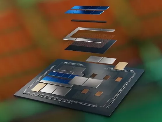
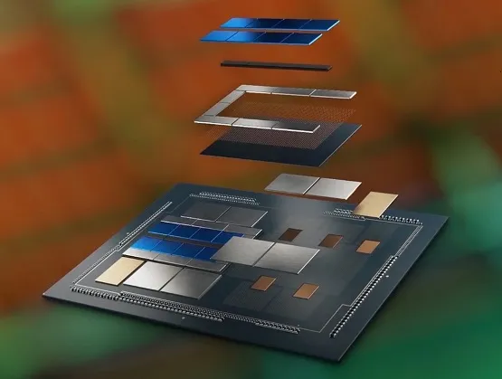
Throughout the current millennium, System-on-Chip (SoC) has been the gold standard for optimizing performance and cost of complete electronic systems. By incorporating practically all the phone’s digital plus analog capabilities onto a single, giant chip, the mobile phone processor serves as a near-perfect exemplar of SoC. But today’s leading integrated circuits (IC) are pushing up against the upper limit of a chip’s size which is limited by the manufacturing equipment’s optical reticle size. This has proven difficult to increase and has grown only slowly over the years. Yet market pressure continues unabated for bigger, more capable electronic systems with more integrated memory, more digital logic, and more analog/mixed signal circuitry. An emerging solution to this tension is 3D and 2.5D multi-die chip assemblies – often referred to as 3D-IC. The key technology breakthrough of 3D-IC is that it makes it possible to spread a system out over multiple, smaller chips that are then assembled close together and interconnected with high-speed, low-power interconnect technologies. By abandoning the need to integrate an entire system on a single SoC and instead allowing it to be disaggregated over multiple chips, 3D-IC enables Moore’s Law to break through the reticle size barrier, improves yield by shrinking the size of individual chips, and makes it possible to mix different process technologies optimized for each function. The Four Engines Driving Semiconductor Design The road forward is not without its challenges, however, and we are seeing design companies making significant efforts to adapt and come to grips with the following four technology and market drivers: The requirement for concurrent multiphysics analysis to ensure reliable and efficient electronic systems The blurring of the lines between silicon and system The need for open and inclusive multiphysics platforms that interoperate with the multitude of design platforms The need for, and value of, bespoke silicon for hyperscalers and system companies Blurring of Silicon and System Design The advent of 3D-IC opens up new horizons for solutions that can be implemented in silicon. But it also forces a closer integration between two distinct technology markets that have co-existed symbiotically for many decades: IC design and printed circuit board (PCB) design. These markets use different tools, different data formats, different manufacturing back-ends, operate at different computational and geometric scales, and focus on different physical concerns. Yet, 3D-ICs share many aspects of both markets: They include monolithic chips but also board-like substrates to stitch the chips together. And in between the two disciplines is packaging, a completely different domain that is requiring companies to re-imagine their design capabilities and flows, as well as their organizational structure. Open, Extensible Multiphysics Platforms The siloed isolation of chip design from PCB design and package design means that each of these markets has developed insular data structures that are ill-suited to deal with the breadth of multiphysics analysis for 3D-IC design. Many different physical disciplines, including computational fluid dynamics, mechanical stress, and electromagnetic radiation, all need to work together based on open and extensible multiphysics platforms. These platforms must embrace the modern cloud compute paradigm and enable an ecosystem by allowing individual design platforms to connect for comprehensive multiphysics analysis. Bespoke Chips Today’s market-leading companies are heavily dependent on technology for their continued success and market differentiation. Everybody from online retailers to telecommunications to social networking companies and hyperscalers are moving away from off-the-shelf solutions and turning to custom-built silicon to give them an edge. Many of these companies are seeking to gain market share by leveraging proprietary AI/ML algorithms trained on their extensive troves of market data – but this requires huge amounts of compute power and specialized chips. Access to high-quality silicon solutions is vital in today’s world and the demand is for continually more complex and powerful electronics. 3D-IC an Inflection Point in Electronic Design To be sure, 3D-IC design is at an inflection point in electronic design and presents major challenges that are realigning the electronic design industry around this new reality. For more insights on this topic from a semiconductor industry leader, please view the Keynote Address 2.5D and 3D – The Road Ahead by Vicki Mitchell, VP Engineering, Arm Central Engineering Systems Group presented at the latest Ansys IDEAS Forum. And for an EDA perspective, please view Successful 2.5D and 3D Multi-die Silicon System Design Using Synopsys’ 3DIC Compiler and Ansys’ Multiphysics Analysis from Synopsys SNUG World 2021. About John Lee John Lee is general manager and vice president of the Ansys Electronics and Semiconductor Business Unit. Lee co-founded and served as CEO of Gear Design Solutions (now Ansys), developer of the first purpose-built big data platform for integrated circuit design. He cofounded two other startups (Mojave Design and Performance Signal Integrity), which successfully exited into companies now part of Synopsys. He holds undergraduate and graduate degrees from Carnegie Mellon University.
Read More
AEM Holdings Ltd, a Singapore-based multinational corporation, is listed in Forbes Asia’s 200 Best Under A Billion 2019 and 2020 spotlighting small and midsized companies in the Asia-Pacific region with sales under $1 billion. AEM clinched the Singapore Business Review Technology Excellence Award 2020 for Analytics-Semiconductor and the Singapore Business Awards Enterprise Award 2019/2020. These achievements are testament to AEM’s vision and innovation and the company’s contributions to the increasingly complex testing of chips in a rapidly evolving technological world. I spoke with AEM CEO Chandran Nair, a new Regional Advisory Board (RAB) member of SEMI Southeast Asia, about the company’s intelligent test and handling solutions, its role in digital transformation, the company’s key role in the smart manufacturing movement and the growth prospects for Singapore’s electronics sector. SEMI: AEM’s application-specific, intelligent system test and handling solutions for semiconductor and electronics companies serve the advanced computing, 5G and AI markets. How do you differentiate your solutions from those offered by competitors? Nair: A key differentiation for AEM is that we work closely with our customers to develop application-specific integrated test and handling solutions that meet their needs in a scalable manner from lab to production. We offer our customers customized, full-stack test and handling solutions that give them the agility to accelerate their delivery cycles and enhance product quality. Over the years, AEM has developed and acquired world-class technologies in instrumentation, test, automation, robotics, optical inspection, high-end thermal control, and software. These technology pillars, along with our deep know-how to customize test and handling solutions using the technology pillars as a platform, enable AEM to meet the fast-changing needs of our customers faced with the challenges of testing heterogeneous and complex devices. In addition to investing in technology, AEM has also invested in delivering application-specific solutions to meet customer demand. Our recently announced acquisition of CEI with its manufacturing capabilities in Vietnam and its specialization in low-volume, high-mix manufacturing increases our geographical reach and our ability to quickly turn application-specific test and handling solutions to be deployed. We have a unique and differentiated approach that enables our customers to test high-performance computing devices, automotive devices, and mobility devices with maximum test coverage, cost-effectively, in a manufacturing environment. Our experience in serving the high-performance computing market that traditionally drives advancements in thermal control also puts us at the forefront of delivering comprehensive thermal management, vision, and deep automation and test solutions for the computing, automotive, and mobility markets. AEM also has a strong instrumentation portfolio, including high-density digital instruments and mixed-signal and protocol-aware instrumentation that is well-suited for ATE solutions for SoC, high-power devices, and CMOS image sensors. Over the last few years, we have also established leadership positions in developing and deploying application-specific test solutions for MEMS devices and offering wafer and frame probing stations suitable for R D, wafer sort, and final test. We form strong partnerships with our customers, provide them with end-to-end support in product development, and take them through the entire life cycle process from concept to mass production. Chandran Nair and Goh Meng Klang, vice president of operations, at the AEM manufacturing site in Singapore. (Photo credit: AEM) SEMI: Digital transformation is powering strong growth of advanced computing, 5G and AI. Will AEM be expanding its AEM manufacturing plants in China, Malaysia and Singapore to meet rising demand for these technologies in the coming years? Nair: In regards to manufacturing, AEM currently has manufacturing facilities in Singapore, Malaysia, the U.S., Finland, and China. With our recently announced acquisition of CEI, we will add manufacturing capability in Vietnam and Indonesia. AEM will continue to expand manufacturing appropriately to give our customers cost-effective solutions while maintaining our proven track record of delivering on time and scaling rapidly in times of crises like the pandemic or geopolitical disruptions. As for advanced technologies, the three key factors that will bring the full potential of 5G to fruition are 1) cost-effective, high-powered processing devices at the edge, 2) easy access to high-bandwidth communications, and 3) cost-effective sensor technology. Semiconductors are the primary drivers of these three key success factors. As devices become more complex and our reliance on semiconductor-powered devices in all aspects of our lives deepens exponentially to include mission-critical applications, AEM’s role is to ensure that our customers' electronic and semiconductor devices are shipped thoroughly tested, safe to use, and highly reliable. It is imperative that, as a testing company, we find innovative ways to help our customers test their products with maximum coverage and minimum cost. To do this, we are focusing our R D efforts and investments to continue building on our key technology pillars to ensure that we stay ahead of the curve when it comes to test and handling solutions. We prepare our customers to test increasingly complex devices manufactured on the latest process node. SEMI: During your career you’ve driven projects in test and automation and more recently robotics solutions for ports, logistics warehouses and transport. With robotics and automation a key part of Industry 4.0, what role do AEM solutions play in powering the smart manufacturing movement? Nair: The smart manufacturing movement is powered by semiconductors, software and increasingly by artificial intelligence (AI). Test is at the heart of the process of ensuring that semiconductor and electronics devices reach the consumer well-tested for reliability. With our vision of enabling A Zero Failure World, AEM addresses the necessity for safe, highly reliable devices. The semiconductor companies themselves are adopting smart manufacturing methods. AEM’s tools are Industry 4.0-ready, and we continue to invest in machine learning and data analytics, which are integral to the future of test. Our tools are automated and feature embedded sensors to provide our customers with data about tool usage, the state of a machine’s health, and more. Our tools are connected to our customers’ manufacturing automation platforms. Additionally, we continue to invest in our ability to better slice and dice test data to understand trends and patterns to help our customers analyze data and make decisions faster. SEMI: You also have experience heading autonomous vehicle projects. With the COVID-19 pandemic hastening digital transformation, do you see an acceleration in the development of fully autonomous vehicles and smart manufacturing? Research and development efforts for autonomous vehicles (AV) continue at a fast pace worldwide. With shutdowns and restricted movement rules globally, the pandemic has hastened digital transformation in many ways. The delivery of goods and services is transforming, and AV will surely play a part, especially in secure environments for autonomous transport. The pandemic has accelerated the development of autonomous vehicles and smart manufacturing technology in automation-friendly environments like factories and ports. SEMI: At the recent Global Technology Summit hosted by SEMI, you spoke about testing innovations to meet the demands of highly complex devices. Please elaborate on innovative testing solutions versus traditional testing? Nair: AEM offers a disruptive and differentiated solution, one that is driving a paradigm shift to asynchronous, modular, highly parallel, smart testing solutions. ​ The traditional approach of ATEs to test increasingly complex devices on advanced nodes has reached a point of diminishing returns as it gets exponentially more expensive to increase test coverage to acceptable levels. Additionally, as devices get more complex and companies are rapidly adopting heterogeneous packaging technologies, the realization that System Level Test (SLT) is necessary is forcing a rethink of the entire test process. AEM’s provides asynchronous, modular, highly parallel test cell solutions that enable each test cell to run SLT, final test, or burn-in all in one system and its ability to handle hundreds of test cells independently with each test cell testing multiple devices. Our solutions suddenly make comprehensive testing of every complex device cost-effective. Freeing us from legacy ATE allows AEM to provide these innovative solutions to our customers. AEM engineering and manufacturing teams in Singapore at work on semiconductor test and handling systems for global deployment at world-class semiconductor facilities. (Photo credit: AEM) SEMI: Singapore seems to be in the sweet spot of digital transformation. Singapore’s industrial production grew 8.6% year-over-year in January 2021, an expansion driven mainly by a surge in sectors including electronics, and more growth is seen in the year ahead. Digital technologies such as 5G technology and cloud computing together with continued demand for work-from-home equipment is behind this growth. What are the growth prospects for the region’s electronics sector? Nair: Singapore is well-poised to benefit from the current digital transformation accelerated by the adoption of these technologies during the pandemic. Being a safe, well-governed country with strong IP protection, excellent infrastructure, and the rule of law, Singapore is in a great position to play a central role in cloud-based services, 5G, and the semiconductor industry. Singapore’s semiconductor sector output is at a record high, and the prospects for renewed growth in the region are very good. SEMI: As a new Regional Advisory Board member of SEMI Southeast Asia, how is your industry experience relevant to the scope of this role? What opportunities lie ahead for the region? Nair: I am honored to represent AEM in the SEMI’s Southeast Asia RAB. The SEMI RAB can influence policymakers with ideas and information on the current and future needs of the industry. I also believe that SEMI Southeast Asia can cultivate a strong innovative semiconductor ecosystem that helps regional and global growth. I look forward to working with other very experienced and accomplished board members. Bee Bee Ng is president of SEMI Southeast Asia.
Read More
As monolithic scaling slows down, the semiconductor industry is increasingly relying on advanced packaging technologies to extend Moore’s law through heterogeneous integration. Higher on-package bandwidth, improved yield resiliency and the need to integrate diverse IP from multiple foundries are driving demand for advanced packaging technologies that address these issues but introduce challenges of their own such as efficient power delivery to all the different domains in a heterogeneous system. SEMI spoke with Kaladhar Radhakrishnan, Intel Fellow at Intel, about heterogeneous system integration trends and new developments in the semiconductor industry. Radhakrishnan shared his views ahead of his keynote at the SEMI Connecting Heterogeneous Systems Summit, 1-3 September 2021, an online event. Join the summit to meet experts from Intel and other key industry influencers. Registration is open. SEMI: What is driving the adoption of electronics and semiconductor devices nowadays and why is the development of new and innovative technologies important? Radhakrishnan: We are living in an increasingly data-driven world where devices have become an integral part of our lives. A recent study estimated that in the United States alone, 13.6 connected devices per capita consume an average of 300 gigabytes worth of data every month. In the workplace, COVID-19 has driven fundamental business changes that has sped up the adoption of digital technologies such as virtual conferencing, remote work, and e-commerce. Organizations are realizing that a high-quality video conference can be an adequate substitute for many in-person meetings. As a result, businesses are accelerating the digital transformation in order to adapt and thrive in this new environment. Five decades of sustained exponential growth in semiconductor performance has conditioned the average digital consumer to expect more from their devices. However, there are some headwinds ahead as traditional scaling slows down and power density rises. Because consumers and businesses are now generating data at a faster rate than they can consume it, technologists need to scale compute, storage, and bandwidth even faster to keep pace. Without investments in research and development of new and innovative technologies to address these challenges, the full potential of this data will go unrealized. SEMI: What forces are heightening the importance of heterogeneous system integration? What are the implications for increased on-package bandwidth, improved yield resiliency and the need to integrate diverse IP from multiple foundries? Radhakrishnan: The semiconductor industry increased transistor density and scaled performance through classical Dennard scaling until the turn of the century. By then, the gate oxide thickness had scaled down to atomic dimensions and the exponential increase in sub-threshold leakage signaled the end of scaling through traditional methods. Since that time, the chip industry has been relying on innovations in transistor materials and structures such as high-k metal gate, strained silicon, and FinFETs to keep pace with Moore’s law. However, this alone will not be sufficient to continue scaling and the industry needs to explore other vectors to augment improvements in transistor technology. Heterogeneous integration through advanced packaging is one key technology that can help drive these gains. Technologies like Foveros can enable device density scaling by creating a 3D stack of multiple die using high-density interconnects. Heterogeneous integration enables chipmakers to move from a monolithic system designed on a single large chip to a heterogeneous system comprised of a number of smaller chiplets. The main benefit of using smaller chiplets is that they improve yield and enable application based customization of the foundry processes. However, if the disaggregation to smaller chiplets is not accompanied by an increase in on-package bandwidth, the power and performance penalties associated with chiplet-to-chiplet communication will hobble system performance. This is why advanced packaging technologies that improve die-to-die communication are key enablers for heterogeneous integration. SEMI: What are some of the key technology challenges in developing heterogeneous systems? Radhakrishnan: The obvious challenge that most people focus on is the need for improved on-package bandwidth. However, as we rely on 3D stacking to continue device scaling at the package level, it is important to comprehend power delivery and thermal challenges as well. Power to the top die has to be delivered through TSVs on the bottom die, which not only adds resistance but also reduces the useful area available on the bottom die. This problem is further exacerbated when we stack more than two die. Excessive noise on the power delivery network can cause timing issues that limit the maximum operating frequency of the transistor. Similarly, when we stack multiple die, we must take into account associated thermal challenges. For example, each interface of the multi-die stack adds thermal resistance, which makes it harder to cool the chips at the bottom. SEMI: What are some of the key global market trends that driving demand for heterogeneous and system-level integration? Radhakrishnan: The number of artificial intelligence (AI) and machine learning applications have grown dramatically due to their ability to solve highly complex problems across a wide range of segments. AI and machine learning models require more memory bandwidth and compute capabilities that are difficult to achieve without some form of heterogeneous integration. Another market trend driving demand for heterogeneous integration is the increasing reliance on custom hardware accelerators. To combat the slowdown in frequency scaling and single-core performance, we have moved to multi-core architectures by tackling the inherent parallelism in our workloads. However, Amdahl’s law tells us that such an approach will hit a bottleneck when we reach the limits of the serial portion of the workload. As these constraints slow the performance of general-purpose processors, the reliance on custom hardware accelerators to boost performance for specific workloads is growing. Heterogeneous integration at the system level with a combination of CPUs, GPUs, FPGAs and other accelerators can optimize system power and performance. SEMI: What solutions is Intel developing to address these market needs? Radhakrishnan: Intel is actively involved in the development of the industry ecosystem for heterogeneous integration. We have developed a number of innovative advanced packaging solutions such as the EMIB and Foveros that are used in products today. Intel is also developing the next generation of advanced packaging technologies, Foveros Omni and Foveros Direct, which will dramatically scale the IO density by using direct Cu-Cu bonding technology. Foveros Omni is a crucial building block technology to enable high-voltage power conversion on the package for efficient power delivery. Intel is uniquely positioned to predict the design needs for future systems and deploy its resources to develop the technology building blocks needed to continue performance scaling. Our IDM 2.0 strategy enables us to leverage our leadership in packaging technologies to design the best products and use the best IP to deliver leading products across a broad range of categories. SEMI: What do you expect from your participation at SEMI Connecting Heterogeneous Systems Summit? Radhakrishnan: I’m hoping to shed some light on some of the new technologies we have been developing at Intel to enable heterogeneous system integration. I also want to bring awareness to the power-related challenges we are facing with heterogeneous systems. I also look forward to listening to what other industry leaders have to say on the topic. Kaladhar Radhakrishnan is an Intel Fellow and a Power Delivery Architect with the Technology Development group at Intel. He plays a significant role in shaping and driving power delivery technologies for Intel microprocessors. His areas of expertise include integrated voltage regulators, advanced packaging and passives technologies. Kaladhar is a two-time recipient of the Intel Achievement Award, the highest Intel honor an individual or small team can receive. He has authored four book chapters, over 40 technical papers in peer-reviewed journals, and has been awarded 35 U.S. patents. He has also served as an adjunct professor at Arizona State University. Kaladhar joined Intel in 2000 soon after receiving his Ph.D. in Electrical Engineering from the University of Illinois at Urbana-Champaign. Serena Brischetto is senior manager of marketing and communications at SEMI Europe.
Read More
Electronics innovation is inching tantalizingly closer to the day when treating neurological disorders such as epilepsy and migraine could be as easy and convenient as dropping into a medical clinic for a minor medical procedure – brain surgery. What today is highly invasive surgery promises to be reduced to a doctor’s office visit as chip engineers work to tether the delicate, complex neurochemical workings of the human brain to the hard wiring of electronics. The goal is to use electrical stimulation to trigger the release of therapeutic doses of natural brain chemicals using small implantable devices in order to restore normal brain functioning, reduce human suffering and help slash the financial burden to economies around the world. The advances come as neurological disorders remain the leading cause of disability worldwide, afflicting up to 1 billion people, a number projected to rise sharply in the years to come, according to the World Health Organization. In 2015, conditions including dementia, epilepsy, multiple sclerosis, Parkinson’s disease and stroke accounted for more than 94 million disability-adjusted life years (DALYS), the number lost globally to ill-health, disability or early death – a total expected to swell to over 103 million by 2030. In the U.S. alone, brain diseases cost nearly $800 billion each year, according to a paper published in the Annals of Neurology in 2017. Bioelectronics Innovation Outpaces Drug Development The trendlines are heightening the urgency to develop new, effective medical treatments, yet traditional drug development alone may not be able to keep pace: The journey to create drugs ready for pick-up at your local pharmacy takes, on average, 10 years from the time they are hatched in the lab. “Unfortunately, pharma is unlikely to help address this problem because drug discovery is becoming slower and more expensive,” George Malliaras, Prince Philip Professor of Technology at the University of Cambridge, noted in his presentation, Electronics on the Brain, at last month’s virtual FLEX 2021 conference. In marked contrast, microelectronics are “becoming cheaper and faster every year.” Dating back to the 1950s with the development of implantable pacemakers to re-establish normal heart rhythms, bioelectronics medicine could help demystify how the brain processes information and lead to more effective treatments for neurological disorders. The field has come a long way since devising cochlear implants to treat hearing impairments in the 1970s, designing spinal cord stimulators to relieve chronic pain in the 1980s and targeting the brain with electrical impulses to help relieve Parkinson’s disease symptoms and neuropsychiatric disorders in the 2000s. ​Deep Brain Stimulation Implants Help Treat Neurological Disorders Deep brain stimulation involves implanting electrodes in the brain through small holes in the skull to send electrical impulses to specific target areas. Used in the U.S. since 1997 to treat Parkinson’s disease, deep brain stimulation can improve motor skills in patients suffering from other conditions too such as dystonia, tremors and epilepsy, enabling them to “function normally, with the flip of a switch,” Malliaras said. Researchers are even testing the technology to treat autoimmune and other disorders not originating in the brain. But the large, rigid electrodes used in the surgery are hostile to the soft, subtle confines of the brain. What’s more, implanting the devices is invasive, with multiple follow-up surgeries typically needed to replace batteries, reposition electrodes or replace deteriorating electrical leads. To overcome these drawbacks, engineers are now designing electronics that can process complex neurological signals to treat brain disorders while conforming to its soft tissue. Malliaras said that means developing electronics capable of interacting with the diverse chemicals the brain uses to bridge the tiny gaps between neurons, called synapses, in order to transmit the neurochemical impulses that give rise to thinking and behavior. Mixed Conductors Form Key Connection Between Electronics and Brain Mixed conductors, materials that can transmit brain signals both ionically and electrically, promise to form this key connection by enabling the development of high-resolution cortical electrodes that monitor neurons without penetrating the brain. They’re also a springboard to the development of flexible pin-sized electronic devices that make neurosurgery much less invasive. That brings new hope for more effective treatments of neurological disorders like epilepsy. Traditionally, the first line of defense against seizures has been antiepileptic drugs, an ineffective treatment since 30% of patients are resistant to the medications, Malliaras said. Another drawback are side effects that include short-term memory loss, fatigue, blurred vision, speech impairments dizziness, nausea and weight loss. Resective surgery – disconnecting the diseased portion of the brain that causes seizures – is often the next option, but is not possible in cases when the procedure would risk damaging circuitry that controls cognition and behavior. Flexible Substrates Fuel Development of Tiny, Expandable Bioelectronics Devices With recent advances, studies on lab rats show that the miniature electrodes designed using flexible substrates made possible by photolithography can conform to the brain’s curvatures and creases to measure the slight electrical signals emitted by individual neurons without penetrating brain tissue and deliver drugs to prevent seizures in animals. Measuring just micrometers in width, these horseshoe-shaped microfluidic devices can pump GABA, a natural neurotransmitter that acts as a brake against neuronal excitability throughout the nervous system, through their minute perforations into the ion exchange membrane of the brain to prevent epileptic seizures. “The data from the research is very exciting, but the path to the clinic is long,” Malliaras said. Still, the findings are a step forward in better understanding the brain and treating its pathologies. Today, microfluidic devices are under development to localize drug delivery in order to bypass the blood-brain barrier and destroy remaining brain cancer cells after a tumor is removed. The devices promise not only to improve cancer treatment since a broad array of cancer drugs can’t cross the protective barrier, but to enable doctors to administer cancer-fighting drugs in smaller doses to help reduce side effects. Implantable electronics today are used to bring relief to sufferers of chronic pain. However, the sizeable paddle-type electrodes involve invasive surgery under general anesthesia and a hospital stay of a few days. An alternative is to implant smaller flexible devices through an outpatient spinal tap with local anesthesia, an approach with its own disadvantages. The devices are less efficient than paddles in delivering electrical stimulation and tend to shift position as the body moves, so are seen as an unreliable solution. That leaves patients to choose between an effective treatment requiring invasive surgery and a less intrusive but less effective alternative. One promising solution combines bioelectronics with soft robotics to enable expandable implants containing microfluidic channels that can be activated mechanically. The device’s malleable paddle electrode can be rolled up inside a needle, inserted with a final tap and then pneumatically unrolled for treatment. While the device so far has been tested only on human cadavers, it could spur the design of a broader category of expandable microfluidics devices that minimize the invasiveness of neurosurgery and get patients back on their feet sooner. The tiny flexible electronics could be available to veterinarians to treat dogs in as soon as next year, Malliaras said, and “hopefully someday in the not-to-distant future they’ll be used to treat human patients.” Michael Hall is a marketing communications manager at SEMI.
Read More
For the first time in its 20-year history, the FLEX Conference dedicated an entire session to the important and timely twin topics of environmental sustainability and power consumption of electronic devices. The event planning committee recognized the urgent need to increase the awareness of how technology and electronics devices can help reduce greenhouse gas emissions (GGE) overall and meet aggressive targets to curb the impacts of climate change. Dr. Christine Ho, CEO of Imprint Energy, delivered the keynote for the session, focusing on the need for powering billions of sensors that will be deployed annually, and their role in reducing fossil fuel emissions through becoming aware of issues, monitoring our resources over time, and intervening early and often to combat waste in multiple sectors and industry. Quoting extensively from the organization Exponential Roadmap Initiative (ERI), Ho noted that “the digital sector has the potential to directly reduce fossil fuel emissions 15% by 2030 and indirectly support a further reduction of 35% by influencing consumer and business decisions and systems transformation.” The initiative’s playbook for reaching net zero carbon emissions by 2050 and limiting global warming to 1.5° Celsius outlines how the digital sector can help remove 13 of the 27 gigatons (GT) of CO2 needed to reach this goal. Ho stated that the rapidly emerging Internet of Things (IoT), devices, software systems, and data insights are the backbone of this digital transformation. The IoT's vast network of sensors can transform multiple sectors, such as the logistics industry, which on an annual basis moves and ships more than 10 billion tons of products worldwide by ships, airplanes, long haul trucks, and train - contributing 17% of GGE and more than 4 gigatons of CO2 annually. Always-connected IoT sensors used by the logistics industry can reduce waste and damage in the supply chain, which is especially problematic for temperature-sensitive and damage prone pharmaceutical and food products, mitigating the need for producing high volumes of buffer inventory to replace damaged goods Noting that the attendees of 20 Years of FLEX Conferences were a big part of the current advancements of low-cost printed, active, shipping tags, Ho said that Imprint Energy’s flexible and thin, Zinc based batteries are ideal for IoT devices, since they boast a significantly smaller carbon footprint than Lithium-Ion (Li-ion) batteries. Imprint Energy is working with systems designers and integrators to design the battery as an integral part of the device package and use low-power strategies to extend device lifetimes. Imprint recommends co-locating battery printing alongside the device integration to further minimize shipping and logistics. When manufactured separately, Imprint’s small footprint, low-operating temperature process line (less than 80°C) provides significant carbon footprint advantages over other technologies. Ho challenged the attendees, saying “we all need to participate in protecting our earth. We need to eliminate waste and contribute to reducing half of our current greenhouse gas emissions by 2030, and we can do that by deploying a global digital skin with more than 100 billion IoT devices in 2030 and up to 1 trillion by 2050. We can minimize the device carbon footprint and maximize its longevity by considering the power capability, as well as design for re-use and re-cycling of the critical materials.” Following Dr. Ho’s presentation, FLEX kicked off a spirited panel discussion with experts from PowerRox, ITN Energy Systems, Birla Carbon, and Auburn University and chaired by Bob Praino and Eric Forsythe, from Chasm Advanced Materials and the Army Research Labs, respectively. The speakers summarized their on-demand presentations and looked at what is being done today to recycle Lithium-Ion batteries, how IoT devices are currently being powered, and drew comparisons between the early days of the Internet and development of the IoT. The speakers generally agreed that the power requirements of wireless cellular and Blue-tooth devices were still too high and run times too short. FLEX 2021 was a virtual event in the 2021 SEMI Technology Series. It was organized by SEMI FlexTech, SEMI NBMC, and NextFlex. Major sponsors included E Ink and Novacentrix. The event covered technical developments in flexible, printed and hybrid electronics, featuring more than 100 presentations and networking opportunities. Technical proceedings are available until March 26 at http://flex.semi.org. Heidi Hoffman is senior director in Corporate Marketing at SEMI.
Read More
Even though microchips continue to get smarter, vital security gaps continue to be exposed through such hack attacks as Meltdown, Spectre, and in recent weeks, Plundervolt. Researchers continue to discover open doors in chip architectures for malicious players to steal increasingly sensitive data, hide the identity of counterfeits, or tamper with electronics systems most anywhere along the global microelectronics supply chain. Today, it’s impossible to have full visibility of the distributed chip making process – from design and fabrication to packaging, testing and delivery. That’s why our industry’s future hinges to a large degree on establishing a hardware root of trust throughout the silicon’s operational lifecycle. Trust but verify! It’s easy to say, but how do we do it?To gain insights, SEMI interviewed Dr. Mark Tehranipoor, currently the Intel Charles E. Young Preeminence Endowed Chair Professor in Cybersecurity at the University of Florida’s Electrical and Computer Engineering Department. A foremost authority on microelectronics security and trust, counterfeit electronics detection, and supply chain risk management, Dr. Tehranipoor will be a keynote speaker at the SEMICON Taiwan Security on Chip Summit, Friday, September 25, where a full program of industry leaders will address key security challenges and solutions involving IoT, systems on a chip (SoCs), integrated circuits, physical unclonable function (PUF) technology, future design, certifications, managed services, and more.For additional insights and to hear Dr. Tehranipoor’s full presentation, register for SEMICON Taiwan 2020, which SEMI is holding as a hybrid event with both a virtual format and an in-show program September 23-25.SEMI: What are the major uncertainties in providing the hardware root of trust within the cyber domain?Tehranipoor: One of the most critical issues we’re dealing with now is loss of control over the process of designing and fabricating integrated circuits and systems. This has happened along with globalization and the movement of supply chain operations overseas to lower costs of nearly all goods, including electronics products and semiconductors. As skill sets, talent, design and fabrication have all shifted offshore, concerns have also risen about security controls across the many different segments of the microelectronics supply chain.For example, when you think about the security of military, space, transportation, power grids, financial or other networks, it becomes a major concern if you cannot trust the underlying electronics system that runs them. New SoCs are also holding more sensitive data around encryption keys, biometrics, personal information or banking data. And as reports escalate about cybersecurity gaps at the electronics part level, it’s increasingly important to establish a hardware root of trust. Today, it’s not enough for a buyer to just call up the design house and verify the electronic ID of an asset. The ID might match, but the device could have been tampered with or replaced with a counterfeit somewhere along its end-to-end journey. Unlike software or networks where problems can be automatically identified, upgraded and fixed, verifying electronic hardware is a costly and time-consuming process, especially when they’re as complex as microchips. It can take months to deconstruct, reverse engineer, inspect, and authenticate a chip. By then, discovery of any security breaches is too late.When addressing the security of electronics systems, there are three important features to keep in mind. First, there’s confidentiality. The device shouldn’t leak information to an unauthorized user. Second, there’s integrity. Unauthorized users should not be able to manipulate an SoC’s sensitive data. The third feature is availability, which can be a result of Denial of Service (DoS) attacks. If the device is under attack and can’t access your online service or network, you must still have security measures for your electronics system to be available in a safe mode while you simultaneously identify the problem, recover from it, and return to normal functions.SEMI: What framework should be followed to establish greater trust and confidence across the entire microelectronics supply chain?Tehranipoor: In the United States, we recognize it may not be possible to bring all manufacturing, design, and delivery teams back to this country and have them certified by the U.S. Department of Defense. You could do some of it, but it would be very costly and complex to bring back all the design, fab, testing, and packaging operations involved with electronics systems and still have complete control.The most practical approach is to make sure we design electronic systems with security and trust in mind from the start. We need to provide security features up front throughout the extended supply chain – into the design flow, fab flow, and out into the field to make it easier and faster for anyone at any point to verify the authenticity of an electronic system as well as identify and mitigate a problem. Finally, we have to remember that we are all in this together – designers, developers, packaging facilities and fabs. We can’t just blame semiconductor manufacturers or any other single entity. As a result, we must be cooperative and collaborative by focusing on this issue as a consortium. Everyone in this ecosystem must come to the table, share best practices, establish standards, and initiate best practices for device to system authentication.SEMI: How can SEMI and the SEMI Electronic System Design (ESD) Alliance help the industry meet these challenges?Tehranipoor: It’s certainly of utmost importance for members of organizations like SEMI and its ESD Alliance committees to jointly develop and adhere to standards or guidelines that establish hardware root of trust across all participants in the global supply chain. At the same time, such alliances should make it a high priority to protect each company’s intellectual property (IP). Collectively, we need resolutions that allow us to develop unique IPs and more easily trace, identify, and verify the authenticity of electronics systems as they flow throughout the end-to-end electronic supply chain. Great efforts are under way and progress is being made. But it’s not enough. Clearly, more needs to be done to establish root of trust standards at the chip level.I can’t emphasize enough the importance of consortia like the SEMI ESD Alliance to create an environment where industry, government, and academia can come together, share best practices and even case studies on how they handled security vulnerabilities and breaches. We understand that not everyone wants to share their security problems, vulnerabilities, or attack surfaces, but learning from each other’s experiences can have a tremendous impact on industrywide progress. If you don’t know what you need to address, you won’t be able to address it when it happens.I also encourage organizations like SEMI to create standards or guidelines that reduce the complexity of microchip designs for security purposes. Realtors often say there are three things to consider in finding a home that will appreciate in value: Location, location, location. To build more secure electronics systems, my mantra is: Automation, automation, automation. Complexity is the enemy of security. By using automation to simplify security mechanisms and detect inconsistencies, it will be easier to find and fix security problems, not to mention lower costs at the same time. SEMI: What will an attendee take away from your talk at SEMICON Taiwan?Tehranipoor: I have a large team of researchers who day and night spot vulnerabilities by attacking and assessing data from different electronic systems set up in our labs. Attendees will see real-world examples and lab animations that show how electronics systems can be hacked most anywhere across the supply chain. They will also learn about step-by-step security solutions we have developed at the microchip level. We need to do a better job of protecting the security of our semiconductor assets and the electronic solutions or services they power. My call to action will be that we need to invest more in research and foster an environment of more open trust and cooperation. We can do this by bringing together different countries, companies, and organizations in the microelectronics ecosystem to overcome this major challenge.Dr. Mark Tehranipoor is currently the Intel Charles E. Young Preeminence Endowed Chair Professor in Cybersecurity at the ECE Department, University of Florida. He is currently serving as Director for Florida Institute for Cybersecurity Research (FICS), National Microelectronics Security Training Center (MEST), CYAN Center of Excellence, and ECI Transition Center. He also serves as Program Director of Cybersecurity for UF Herbert Wertheim College of Engineering. His current research interests include IoT security, hardware security and trust, and reliable circuit design.Samer Bahou is senior manager of corporate communications at SEMI.
Read More
In the first part of this double feature, we looked at the automotive industry’s transition toward a mobility ecosystem and the shifting business model perspective from selling vehicles to miles. At the core of these changing dynamics are four trends represented by the acronym ACES: Autonomous, Connected, Electric, and Shared mobility. Each of these trends is largely enabled by microelectronics through computer processors, sensor units, and communication architectures. Part 2 of this series explores the business opportunities at the transition from automotive to mobility, and the specific role SEMI can play as a natural bridge between the two ecosystems.Electronics and Software as Drivers for Automotive InnovationThe ACES trends represent an acceleration of the shift in automotive from the industry’s traditionally strong focus on mechanics and hardware toward electronics and software. This transition to electronics and software as drivers for automotive innovation already started in the 1970s with electronic fuel injection, anti-lock brakes, trip computers, and many other attributes that are now considered standard features. As a result, there are now hardly any automotive systems that are not computer-controlled. A vehicle without power windows and locks, electronic climate control, or MEMS-reliant airbags are basically unimaginable in many markets.As shown in the graphic[1] depicting the electronics share of total vehicle cost, the numbers paint a clear picture of the continued growth of electronics over time, with a 44% share today expected to grow to 50% by 2030. McKinsey Company estimates the automotive software and electrical/electronic (E/E) components markets combined will grow at a 7% CAGR from USD 238 billion in 2020 to US$469 billion by 2030[2].The assumption of continued and sustained growth presents a promising outlook for semiconductor and sensor content in vehicles over the next decade, which is particularly strong in the electrification space. Hybrid electric vehicles (HEVs) already contain $900 worth of semiconductor content, and battery-based electric vehicles (EVs) contain $1,000 worth of semiconductors – much higher than the average of approximately $450 of content in conventional vehicles[2]. Other business opportunities in the mid-term (3-5 years) include software, battery technology, infrastructure (charging stations, other hardware components, etc.), as well as vehicle-to-vehicle (V2V) and vehicle-to-environment (V2X) communication. These technologies also demonstrate how the industry’s business focus is expanding beyond the confinement of an individual vehicle to increasingly contemplating the evolving ecosystem around it, resulting in real mobility solutions. Image credit: Continental AG This creates significant opportunities for a large number of SEMI members in the semiconductors and sensors business by connecting them with new customers and partners in the automotive and mobility supply chains, primarily vehicle manufacturers and Tier 1 suppliers, and together realizing new business in new automotive applications such as: Autonomy, including ADAS (GPUs, LiDAR, radar, camera, accelerometers...) Connectivity (link to outside infrastructure and in-cabin devices, roadside units...) Electrification (power electronics, battery monitoring, H2 detection in fuel-cell...) Sharing (customizable vehicle interior, trackable mobility devices such as scooters...) In-cabin experience (media systems, displays, VR/AR, occupant detection...) Vehicle architecture (flex-ray, automotive ethernet, diagnostics, smart parts...) Safety and security (HW/SW firewall, parts authentication, upgradability...) In these partnerships, the vehicle manufacturers and component suppliers clearly benefit from leveraging semiconductor capabilities including: Device and system reliability/robustness/quality (“Zero Defect”), which creates opportunities for new SEMI Standards (e.g. wafer-to-device/system traceability) New design architectures for added functionality, safety and security New packaging solutions (automotive OEMs are already participating in the Heterogeneous Integration Roadmap, seeking to collaborate with device manufactures and Original Semiconductor Assembly Test (OSAT) companies to reduce costs and differentiate on automotive-grade solutions Sensors and imaging (cameras) SEMI Smart Mobility Initiative – Connecting Mobility and ElectronicsSEMI launched its Smart Mobility Initiative in 2018 based on the mandate of providing “SEMI members with access to new business opportunities and collaborative platforms in the automotive electronics supply chain.” The initiative is currently focused on synchronizing the automotive and microelectronics supply chains for automotive electronics innovation – in particular semiconductor devices, sensors, and related products manufactured for this space and sold to vehicle OEMs and Tier 1s. To facilitate closer dialogue among stakeholders from this combined ecosystem, SEMI formed the Global Automotive Advisory Council (GAAC) which now has five regional chapters and represents dozens of companies. Collectively, GAAC members discuss and act on a wide range of topics, from Silicon Carbide (SiC) standardization to new design architectures and closing the OEM requirement gap.While continuing to build on the strong automotive foundation, SEMI’s Smart Mobility Initiative is now expanding its reach and scope of activities to broader mobility themes, such as infrastructure and battery technology and Smart City, to infuse SEMI member communities and the GAAC with new stakeholders and new ideas. These are exciting times!Please contact Bettina Weiss, Chief of Staff at SEMI, at [email protected] for further information about SEMI’s Smart Mobility Initiative, the Global Automotive Advisory Council, and how SEMI can help your organization navigate electronics in the automotive industry to drive innovation in the mobility space.[1] see graphic, created with data from NXP / Freescale[2] Source: McKinsey Company, 2019Microelectronics Power the Future of Mobility – Part 1: Autonomous, Connected, Electric and SharedBettina Weiss is Chief of Staff and Global Smart Mobility Lead at SEMI. Sven Beiker is Smart Mobility Consultant at SEMI.
Read More