downloadGroupGroupnoun_press release_995423_000000 copyGroupnoun_Feed_96767_000000Group 19noun_pictures_1817522_000000Member company iconResource item iconStore item iconGroup 19Group 19noun_Photo_2085192_000000 Copynoun_presentation_2096081_000000Group 19Group Copy 7noun_webinar_692730_000000Path
Skip to main content
Default Banner Image

18FDS

Since the beginning of the year, there’s been a steady stream of excellent news around Samsung Foundry’s 28FDS, their highly successful 28nm FD-SOI offering. Let’s take a look at what’s been happening, as things do seem to be accelerating. By way of reminder, they announced the industry’s first eMRAM (embedded MagnetoResistive RAM) testchip tape-out milestone on 28FDS in September 2017 (you can read the press release here) - which was just a year after they had announced mass production of 28FDS process technology.At the end of 2018, Arm announced the industry’s first Embedded MRAM (eMRAM) compiler IP built on Samsung Foundry’s 28FDS process technology. Follow that with this announcement at the beginning of 2019: Soitec Expands Collaboration with Samsung Foundry on FD-SOI Wafer Supply. The two companies announced that Samsung had secured a high-volume supply of FD-SOI technology to meet industry's current and future demands especially in consumer, IoT and automotive applications. In March came two more big announcements. First: Samsung Electronics Starts Commercial Shipment of eMRAM Product Based on 28nm FD-SOI Process. As they noted in the PR, “Samsung’s 28FDS-based eMRAM solution offers unprecedented power and speed advantages with lower cost. Since eMRAM does not require an erase cycle before writing data, its writing speed is approximately a thousand times faster than eFlash. Also, eMRAM uses lower voltages than eFlash, and does not consume electric power when in power-off mode, resulting in great power efficiency.”Hard on the heals of that came the news that Arm and Samsung Announce IP Platform including eMRAM for 18nm FD-SOI. At the SOI Consortium’s Silicon Valley Symposium in April, Tim Dry (he’s Samsung’s Director of Foundry Marketing for Edge and End Point), gave a terrific presentation. Entitled Samsung’s FDS with MRAM: Enabling Today’s Innovative Low Power Endpoint Products, it details the company’s FDSOI roadmap for the IoT Endpoint Platform (and yes, you can download in its entirety). Then in May at the big Samsung Foundry Forum in Silicon Valley, Arm, in collaboration with Samsung Foundry, Cadence, and Sondrel, demonstrated the first 28nm FD-SOI eMRAM IoT test chip and development board. The Musca-S1 test chip demonstrates a new choice in SoC design for IoT solutions, said Arm. (Sondrel, btw, is Europe's largest independent IC design consultancy.)In parallel, Cadence announced: Cadence Custom/AMS Flow Certified for Samsung 28nm FD-SOI Process Technology. Especially aimed at digitally-assisted analog designs, what’s new here is that the Cadence custom and analog/mixed-signal IC design flow is now Samsung Foundry certified for 28FDS. Samsung’s 28FDS PDK techfile is Mixed-Signal OpenAccess ready, enabling customers to deploy OpenAccess-integrated, fully interoperable Virtuoso-Innovus implementation flows. For its part, at its Foundry Forum, Samsung unveiled extensions of the company’s FD-SOI (FDS) process and eMRAM together with an expanded set of state-of-the-art package solutions. They indicated that the development of the successor to the 28FDS process, 18FDS, and eMRAM with 1Gb capacity will be finished this year.And finally, companies like NXP are shipping exciting new products fabbed on Samsung’s 28FDS. Ron Martino, VP GM of NXP’s i.MX Application Processor Product Line covered key products in his presentation at the SOI Consortium’s Silicon Valley Symposium (see our coverage here). Among them: the i.MX7ULP for long battery life with 2D 3D graphics for wearables and portables in consumer and industrial applications; the i.MX 8 and 8X subsystems for automotive and industrial applications; and the i.MX RT series of “cross-over” processors. The i.MX RT ULP (real-time, ultra-low-power) series, which Martino says is the “new normal”, deals with a high number of sensor inputs. The i.MX RT 1100 MCUs, which have been qualified for automotive and industrial applications, are breaking the gigahertz performance barrier.In July, linuxgizmos.com reported that, “In June, NXP began volume shipments of its super power-efficient i.MX7 ULP, which it announced in 2017. The SoC is billed as the most power-efficient processor on the market that also includes a 3D GPU. […] the ULP version includes a 3D graphics capable Vivante GC7000.” (Vivante, btw, is a VeriSilicon company, which is an SOI Consortium member and a leading proponent of FD-SOI design and IP in China and worldwide.) This is leading to some really nice wins for NXP. For example, they’ve got Amazon's Alexa Voice Service (AVS) leveraging the i.MX RT crossover processor, enabling developers to quickly and easily add Alexa voice assistant capabilities to their products. The RT series has rapidly been expanded, with versions for voice-controlled devices and offline face and expression recognition capabilities for smart home, commercial and industrial devices.Also announced this summer: NXP and Microsoft Bring Microsoft Azure Sphere Security to the Intelligent Edge with a New Energy-Efficient Processor. That collaboration includes development of a new crossover applications processor in NXP’s i.MX 8 series integrating Microsoft’s Azure Sphere security architecture and Pluton Security Subsystem. Their customers “will be able to harness the high-performance and energy efficiency of NXP’s i.MX 8 applications processors combined with Microsoft’s unequaled security and assurance provided by Azure Sphere certified chips”. As Martino concluded in his presentation, “The future of embedded processing [is] enabled by FD-SOI.” And Samsung Foundry’s FD-SOI offerings are clearly a massive enabler of that future.
Read More
Editor's note: Arm and Samsung Foundry are extending their collaboration on FD-SOI, which they'll be highlighting at the SOI Consortium's Silicon Valley Symposium April 9th. In the meantime, Arm Senior Product Marketing Manager Umang Doshi described the range of projects in a recent Arm Community / Developer physical IP blog. We thank Arm for sharing this blog with ASN readers.~ ~~ Samsung Foundry and Arm FDSOI collaboration announced By Umang Doshi The challenge with designing at newer and more advanced process nodes is that things generally don’t get less complex and expensive, much as we might want this. Still, the upside to each new process node, generally, is that you can build more highly efficient and targeted devices to address more markets and applications in a timely fashion. 
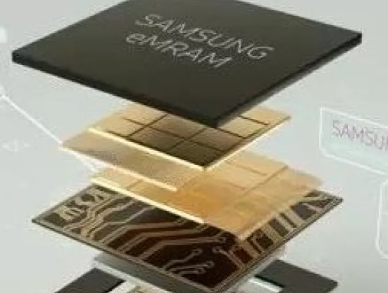
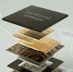
For the complexity and cost challenges, however, there’s good news: Arm and Samsung Foundry just announced a comprehensive, foundry-sponsored physical IP platform, including an eMRAM compiler at 18FDS (18nm FDSOI). In addition, the Arm offerings for 18FDS include three POP IP packages for Arm Cortex-A55, Cortex-R52 and Cortex-M33 processor IP. The platform will help drive new leading-edge designs in power-sensitive applications in 5G, artificial intelligence (AI), automotive, Internet of Things (IoT), and other market segments. It’s the industry’s first, fully comprehensive physical IP platform that includes an eMRAM compiler at 18FDS. 28nm: Before the breakthrough One of the most widely embraced nodes, 28nm the so-called “forever node,” has done wonders for industry innovation over the years. However, leakage power is still challenging for planar transistors. Engineers deployed high-K metal gate (HKMG) at 28nm, to combat leakage, but it’s still an issue. That’s because the channel underneath the gate is too deep and too far from the gate to be well-controlled, which results in higher leakage power. Solutions for the leakage issue have prompted designers to embrace FinFETs and FDSOI (fully-depleted silicon-on-insulator) with thinner channels that enable greater control by the gate. Indeed, FDSOI is gaining traction in the market place. By construction, 28nm FDSOI enables much better transistor electrostatic characteristics versus conventional bulk technology. 28nm FDSOI offers: Wide Forward/Reverse Body-bias range and flexible Poly bias (PB) range to tradeoff power/performance. Better performance and power than bulk process technology. Better resistance to radiation and SER. Less sensitive to variability because there’s no channel doping. Ultra-low power voltage (operating at low voltages in the hundreds of millivolts range). Easy migration from bulk versus the previous SOI version, PDSOI (partially-depleted silicon-on-insulator), required unique timing and power models. What’s more, there are cost benefits today and more forecast for the future. Arm and Samsung Foundry extend FDSOI leadership from 28FDS to 18FDS In 2018, Arm announced the industry’s first Embedded MRAM (eMRAM) compiler IP built on Samsung Foundry’s 28FDS process technology. Since the announcement, Arm has engaged with several Samsung Advanced Foundry Ecosystem (SAFETM) partners on a landscape-changing collaboration to deliver the industry’s first 28FDS eMRAM-enabled IoT silicon system demonstrator telling the Arm IoT story on Samsung Foundry silicon. Coupled with Arm’s IoT ecosystem, Pelion IoT Platform and Platform Security Architecture (PSA) solutions, this 28FDS eMRAM-enabled IoT demonstrator will showcase a new-generation of secure and energy-efficient IoT edge devices which integrates software stacks offering secure boot, firmware updates, on-chip storage, chip to cloud communication and device/software provisioning. The combination of 28FDS and eMRAM non-volatile memory brings new opportunities for a new class of highly integrated and energy-efficient designs. We’re thrilled that Samsung Foundry has extended its successful collaboration on FDSOI technology from 28FDS process to 18FDS. With the new platform, 18FDS is a cost reduction solution with lower power and same back end of line (BEOL) as 14nm FinFET. It has RF and eMRAM support to enable the widest range of different applications. “18FDS is the next-generation node on Samsung's FD-SOI roadmap with enhanced power, performance, and area (PPA)," said Jaehong Park, executive vice president of Design Platform Development at Samsung Electronics. “The relationship between Samsung Foundry and Arm stretches back more than a decade and has helped put the right design technology in the hands of the world’s leading designers. The enhanced PPA from our 18FDS process combined with Arm cores and Artisan Physical IP will again bring the cost and time-to-market advantages to enable the competitive and differentiated SoC designs.” Highlights on Arm-Samsung 18FDS platform Includes seven memory compilers, three logic libraries, two (1.8 and 3.3V) GPIO libraries, three POP IPs and the eMRAM memory compiler. Supports automotive AEC-Q100 Grade 1 design requirements, and comes with ASIL-D support and a complete automotive safety package. Utilizes back biasing supported by the FDSOI technology to help achieve low leakage by using reverse body-bias technique or a performance boost using forward body-biasing. This is a key differentiation of 18FDS platform. Supports Logic Corner Generator (LCG) and Memory Compiler Corner Generator (MCCG). LCG and MCCG products allow designers to generate custom corners with body-bias voltages to take the maximum advantage of body biasing power-performance flexibility. 18FDS will help enable the development of new devices connecting consumers in entirely new ways, whether it’s in AI, 5G mobile, automotive or other areas. The platform will be available in late 2019. Arm's Physical Design Group has a track record of successful implementations with Samsung Foundry across multiple generations of process nodes and products. Besides 28/18FDS, Samsung Foundry and Arm also have 14LPP/LPC, 11LPP, 7LPP and 5LPE platform collaborations. Interested in knowing more about Artisan Physical IP at 28/18FDS? Come join us at SOI Silicon Valley Symposium on April 9 at Double Tree by Hilton, San Jose, California. During the event, you will have the opportunity to hear how Arm and other industry leaders work together to accelerate the adoption of FDSOI technologies including products and applications. Alternatively, you can also reach out to us with your inquiry.
Read More
Per Arm, the industry's first eMRAM compiler IP is now on Samsung's 28nm FD-SOI technology. The announcement was made in a post by Kelvin Low, VP Marketing for ARM's Physical Design Group (read it here). He said that ARM has successfully completed their first eMRAM IP test chip tapeout. The Arm eMRAM compiler IP will be available from 4Q 2018 for lead partners. Samsung Foundry’s 28nm FD-SOI process technology is called 28FDS. eMRAM (which stands for embedded MagnetoResistive RAM) is a novel non-volatile memory (NVM) option positioned to replace incumbent NVM eFLASH, which has hit its limits in terms of speed, power, and scalability. Arm's new eMRAM compiler IP gives Samsung's 28FDS customers the flexibility to scale their memory needs based on the complexity of various use-cases, explains Low. “What drives the cost-effectiveness of this compiler IP is that eMRAM can be integrated with as few as three additional masks, while eFlash requires greater than 12 additional masks at 40nm and below,” he says. “Also, the eMRAM compiler can generate instances to replace Flash, Electrically Erasable Programmable Read-Only Memory (EEPROM) and slow SRAM/data buffer memories with a single non-volatile fast memory – particularly suited for cost- and power- sensitive IoT applications.” [caption id="attachment_11972" align="alignleft" width="300"] A key slide shown by Arm at the 2017 SOI Consortium's Silicon Valley Symposium (Courtesy: Arm and the SOI Consortium)[/caption] At the SOI Consortium's 2017 Silicon Valley Symposium, Arm said that they were stepping up their support of FD-SOI (read about that here) – and clearly they are! At that event, Arm VP Ron Moore gave a great presentation, which is freely available on our website: Low Power IP: Essential Ingredients for IoT Opportunities. Samsung, btw, has been offering 28FDS for about three years now. (ASN did a 3-part interview with Kelvin Low back in 2015 when he was a senior director of marketing for Samsung Foundry. It's still a useful read – you can get it here.) As of last fall, Samsung said it had taped out more than 40 products for various customers. And at the SOI Consortium's 2018 Silicon Valley Symposium, Hong Hoa, SVP said they'd already taped out another 20 this year (read about that here). https://youtu.be/EB14K8Gq5-w Samsung says the write speed of their eMRAM is 1000x faster than eFlash. They actually announced the industry's first eMRAM testchip tape-out milestone on 28FDS in September 2017 (you can read the press release here). They also did an eMRAM test chip with NXP. (BTW, Samsung has a really nice video explaining their eMRAM offering – you can see it above or on YouTube here.) As noted in ASN's Silicon Valley 2018 symposium coverage, the basic PDK for the Samsung 18nm FD-SOI process (18FDS) will be available in September 2018, with full production slated for fall of 2019. It will deliver a 24% increase in performance, a 38% decrease in power, and a 35% decrease in area for logic. RF for the 18FDS platform will be ready by the end of this year, and eMRAM beginning in 2019.
Read More
Big News: Samsung has officially revealed that their next FD-SOI node is 18nm. The announcement was made at the recent Samsung Foundry Forum, which showcased a number of new technologies that the company says will help enable the development of new devices connecting consumers in entirely new ways. (You can read the full press release here.) Samsung also announced new features for its 28nm FD-SOI offering, which is called 28FDS. Noting that it is well suited for IoT applications, Samsung said it will gradually expand its 28FDS technology into a broader platform offering by incorporating RF and eMRAM(embedded Magnetic RAM) options. 18FDS is the next generation node on Samsung’s FD-SOI roadmap with enhanced PPA (Power/Performance/Area). [caption id="attachment_10762" align="alignnone" width="705"] Kinam Kim, President of Samsung Electronics’ Semiconductor Business, introduces the company’s newest foundry process technologies and solutions. (Courtesy: Samsung)[/caption] The FD-SOI news was part of an announcement covering Samsung's newest process technology roadmap. “The ubiquitous nature of smart, connected machines and everyday consumer devices signals the beginning of the next industrial revolution,” said Jong Shik Yoon, Executive Vice President of the Foundry Business at Samsung Electronics. “To successfully compete in today’s fast-paced business environment, our customers need a foundry partner with a comprehensive roadmap at the advanced process nodes to achieve their business goals and objectives.”
Read More