They're calling it, “The most advanced, lowest power-consuming GPU-enabled MPU on the market.” It's NXP's new i.MX 7ULP general-purpose processor, and it's on 28nm FD-SOI. They've got a nifty video summing it all up – you can watch it here.
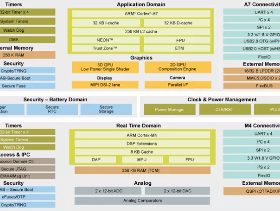
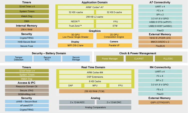
[caption id="attachment_10388" align="alignleft" width="300"] NXP is first to market with a general-purpose processor on FD-SOI: the i.MX 7ULP. It's got both ultra-low power consumption and rich graphics for battery powered applications. (Courtesy: NXP)[/caption]
With the i.MX 7ULP, NXP is first to market with an FD-SOI applications processor offering the industry’s lowest power consumption. The debut was made at the recent Embedded World Conference in Nuremberg, Germany, and it made a big splash in media across the globe. (Read the full press release here.) In deep sleep mode, it boasts power consumption of just 15 uW or less: 17 times less than previous (and highly successful) low power i.MX 7 devices. Dynamic power efficiency is improved by 50 percent on the real-time domain.The i.MX 7ULP applications processor family is currently sampling to select customers. Broader availability of pre-production samples is scheduled for Q3 2017.Hello, IoT!The high-performance, low-power solution is optimized for customers developing applications that spend a significant amount of time in standby mode with short bursts of performance-intense activity that require exceptional graphics processing. Sounds like IoT – and indeed it is, and more.With the i.MX 7ULP, NXP's targeting wearables, portable healthcare, smart home controls, gaming accessories, building automation, general embedded control and IoT edge solutions. Bottom line: it's designed to enable ultra-low-power and secure, portable applications – especially those demanding long battery life. (Read the current fact sheet here.)The detailsThe i.MX 7ULP features an advanced implementation of the ARM® Cortex®-A7 core, the ARM Cortex-M4 core, as well as a 3D and 2D Graphic Processing Units (GPUs). It's got a 32-bit LPDDR2/LPDDR3 memory interface and a number of other interfaces for connecting peripherals, such as WLAN, Bluetooth, GPS, displays, and camera sensors.
[caption id="attachment_10387" align="alignnone" width="834"] (Courtesy: NXP)[/caption]
NXP says this new design, based on FD-SOI’s lower voltage capability, enables rich user experience through extremely power-efficient graphics acceleration, a fundamental requirement in many of today’s consumer and industrial battery-operated devices that incorporate robust graphic interfaces. Further enablement includes rich Linux or Android ecosystem with the real-time capability supported by FreeRTOS.Leveraging body biasing and moreNXP credits the design’s extreme low leakage and operating voltage (Vdd) scalability to that FD-SOI specialty: reverse and forward body biasing (RBB/FBB) of the transistors, and its smart power system architecture.In presenting the new i.MX 7ULP to the tech press, the company highlighted the following FD-SOI design advantages:
Large dynamic gate and body biasing voltage range
Domain and subsystem optimization with custom standard cell library with mixed voltages
Low quiescent current (Iq) bias generators
Enhanced ADC performance with unique FD-SOI attributes
Fail Safe I/O for simplified low power system design
To that, add a note about security. As the chip's fact sheet says, “The processors deliver hardware-enabled security features that enable secure e-commerce, digital rights management (DRM), information encryption secure boot, and tamper detection.” Those are just the sort of things that demand the bursts of high performance that dynamic forward body biasing delivers where and when it's needed.Samsung fabs, Verisilicon adds IPTwo other SOI Consortium members – Samsung and Verisilicon – are particularly pleased with NXP's results.“We are excited that NXP is the first to bring the benefits of FD-SOI (28FDS) technology to the general purpose market,” says Ryan Lee, VP of the Foundry Marketing Team at Samsung Electronics. “28FDS technology will satisfy a growing and critical need for ultra low power designs that require power-performance at very low voltages. We plan to evolve 28FDS technology to a differentiated low-power single platform by implementing RF and embedded Non-Volatile Memory (eNVM) solution for our customers’ success.”NXP’s processor design enables robust low power graphics for the IoT and wearable markets through two graphic processor units (GPU) from Vivante: the GC7000 NanoUltra 3D GPU with a low power single shader, and the GC320 Composition Processing Core (CPC) for 2D graphics. The 3D GPU plays a critical role in enabling rich 3D based user interfaces, while the CPC can accelerate both rich 3D and simpler 2D user interfaces. Processors based on the combination of the two GPUs enable efficient display systems which offload and significantly reduce system resources, in turn providing rich user interfaces at low power levels to extend the battery life of devices.“Our 3D GPU is a result of a joint collaboration between Vivante and NXP to deliver industry-leading 3D capabilities with the lowest power consumption,” said Wei-Jin Dai CEO at Vivante Corporation and Chief Strategy Officer and GM of the IP Division at Verisilicon. “The power savings from using the right GPU in an ultra low power processor is one of the major attributes and advantages of the architecture.”So, now shall we dig in a little deeper into the “why FD-SOI” question? Read on in Part 2 of this article.-- By Adele Hars, ASN Editor-in-Chief