downloadGroupGroupnoun_press release_995423_000000 copyGroupnoun_Feed_96767_000000Group 19noun_pictures_1817522_000000Member company iconResource item iconStore item iconGroup 19Group 19noun_Photo_2085192_000000 Copynoun_presentation_2096081_000000Group 19Group Copy 7noun_webinar_692730_000000Path
Skip to main content
Default Banner Image

SOI Consortium

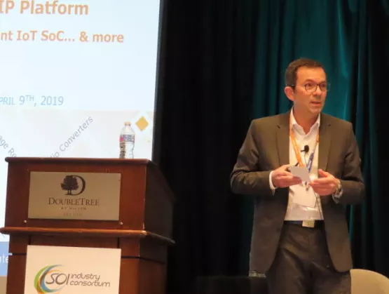
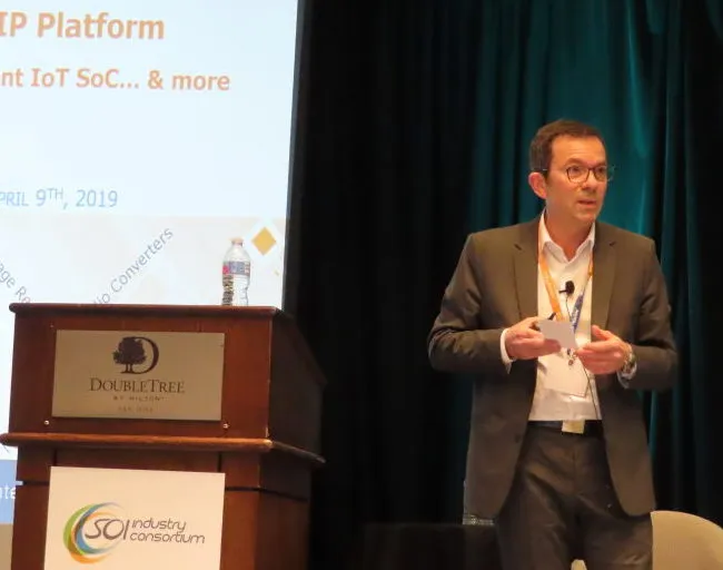
VeriSilicon provides platform-based, all-round, one-stop custom silicon services and semiconductor IP. For two years running, they’ve been the #1 Chinese IP provider and well into the Top 10 worldwide (per IPnest 2020). They’re also an FD-SOI design powerhouse. Founded in 2001, VeriSilicon first began work on FD-SOI in 2013. Now they’re headed for listing on the Shanghai STAR exchange. SOI News talked to President CEO Dr. Wayne Wei-Ming Dai about his company’s innovative business model, and opportunities for FD-SOI.SOI News (SN): You call the VeriSilicon business model “SiPaaS”, for Silicon Platform as a Service. Can you tell us what that means? Is it particularly well-suited to designs based on FD-SOI? Dr. Wayne Wei-Ming Dai (WD): We see SiPaaS as the third transformation in the semiconductor industry. If you take a minute to look at the evolution, first was the IDM model of the 1960’s and 70’s, largely based in the US and Japan and driven first by the US military, then home appliances and consumer electronics. The second transformation was the foundry model, driven heavily by the PC and cellular communication, with a geographic center heavily based in Taiwan and Korea. That solved the CAPEX challenge. Now with the IoT, we solve the OPEX – operational expenses – challenge. Although 60% of our business comes from outside China, we do see particularly good opportunities for China. With AI and AIoT, there’s a lot of custom designs. You have a new model with the chip as a system, with lots of IP – but it also is much more expensive. The VeriSilicon SiPaaS model covers everything from IP to final tape-out, delivers packaged and tested parts, and that accelerates time to market and saves money. If you consider the share of R D expenses as a percentage of chip revenue, for leading fabless companies, they can be 20-30%, and you need to have a gross margin of 50% and higher. But if your gross margin is 40% or below, you might out of business. The VeriSilicon model seeks to transform the design-heavy model, where designers use their own IP, to the next wave, which is design-lite. When you’ve got a design-lite model for A/IoT, you don’t need such a big team. This is the third transformation. You first saw this starting in a major way in Israel, where going to design-lite enabled fabless companies to move very quickly. But you still need IPs, and for those working under a traditional model, we have those. In SiPaaS, we offer IP platforms. Chip design is kind of like building a house. If you want, we can just give you the kitchen – so that’s some specific IP. But we can also give you the entire house. The IPs form the solutions. For each type of application, there are similar IPs that need to be integrated. Sets of IPs form subsystems for IoT, automotive, medical, wearables, audio, video, etc. There are no boundaries on the platforms, but each have typical elements. In this industrial transformation, and now especially for AIoT, you’ll need many more chips in many different places. We have a lot of IP that we created organically, but we also made some major acquisitions over the years. For example, 13 years ago we bought a Dallas based DSP division from LSI Logic. Our design-lite platform approach plays particularly well in FD-SOI, where designers want to maximize the advantages of the technology. Remember that much of the original IP for FD-SOI comes from ST or Samsung. When Samsung first licensed 28nm FD-SOI from ST, we got a whole set of 28nm FD-SOI IP from ST with modification rights. So we started to play with them. Then that IP went to Synopsys. We have modified, optimized and customized it for customers. And with GlobalFoundries’ 22nm FD-SOI, when the IP comes out, we're the first ones invited to test it. So we focus on those IPs. We do benchmarks on ARM and others. And we’ve designed our own IPs for RF and more. We’ve done the body biasing circuits and software control, so we support design methodologies. People often ask us to show them how good FD-SOI is. So we do a lot of benchmarking. At 28 bulk, we can do apple-to-apple comparisons. And 28 bulk or 22 FD-SOI, it’s the same team, so we can do those comparisons, so they can compare the two nodes. And we’re partnering with more 3rd party IP companies – including smaller players – providing FD-SOI IP, which is great. [bctt tweet="Our design-lite platform approach plays particularly well in #FDSOI, where designers want to maximize the advantages of the technology - @VeriSilicon CEO Wayne Dai #IoT #edgeAI #wearables" username="SOIConsortium"] SN: You have been a very vocal champion of FD-SOI. Why? WD: We’re not against FinFET – that a really big part of our business and we’re very advanced in it. We were the first to do a tape-out on Samsung’s 7nm UV FinFET test chip and are working on 5nm. While overall we tape out over 30-50 chips a year, we are foundry neutral. But we recognize that FinFETs are not for everything: there are some things that FD-SOI does much better. Integrating RF, for example – it’s not impossible but it’s not natural in FinFET. Yes, if you’ve got a big digital chip running at high speed most of time, FinFET is better. But if you’re running high speed some of time, say around 20%, especially integrating RF, FD-SOI is better. And back biasing is impossible in FinFET. In the end, we “walk on two legs”. SN: What do designers need to know about FD-SOI? WD: Body biasing can sound complicated, but the thing is, you don't play with each transistor. In theory, you can control each transistor with body bias, but in reality, you do it region by region. With body biasing, you can dynamically make different parts of the chip behave differently. This is key. Some parts are reverse biased. Some parts are forward biased. You play with this block by block, and kick it in as-needed by software after the chip comes back. So in IoT, for example, where it's very serious low power, you may want to shut down certain parts when you're not using them, while other parts always need to be on. If you choose one of our platforms, we’ve taken care of that. There may be parts you only need to bring up and run at high-speed for certain tasks. So body biasing gives you all sorts of controls. With FinFETs you can't do that, you can just play with voltage scaling. You can drive up the speed – the dynamic power – when needed with forward biasing. During that time, you're not really worrying about leakage power because when the task is done you can completely shut down those parts again. It also changes tape out. Typically designers do worst case. But you might not need to design for the worst case: you leave too much on the table. With body biasing, if you solve for typical, when the chip comes back, you can tune and make adjustments post-silicon. So you can do an aggressive tape-out, which is much more effective than starting off with a worst case. True, if you sign off worst case, your chip can always run very fast, but sometimes you don't need that. And in order to solve for worst-case, you put in a lot of buffers or whatever for timing closure, which is unnecessary effort. What's more, for different applications, the worst case can be different: some applications may need some higher speeds and sometimes less. If you solve for typical, then depending on the application you can software-tune the device. In the past, you never had that kind of thing. With body biasing in FD-SOI, you can solve for typical, so you can save a lot of area and a lot of design cycle in terms of timing closure, in terms of use of buffers. If silicon comes back, and it's missing something – say you need it to go a little faster – I’ve done body biasing, so I adjust the timing. Most times it's probably ok, it's good enough. Of course, some applications you need some combination of fast and slow, and you can leverage the body-biasing post silicon to change what's fast and what's slow on the fly. Like in wearables, power is very critical – some parts are always on, and some parts are sometimes on. For the parts that are always on, you need to reduce the leakage, and you do that with reverse body biasing. For other parts, you bring them up and you run as fast as you can for a short period of time – in this case leakage isn't as important because most of the time it's shut down. But dynamic power is important. High performance is important. For that part you need forward biasing. With different parts of the chip, you can play with different things. Before, you had to do this before tape-out, and sometimes had to do worst-case, which should never happen: you leave too much margin on the table, because after silicon you couldn’t do anything. But now with body biasing in FD-SOI, you have the capability – you don't need to do worst case – if needed you can always adjust. And for different applications in the chip, you might need a different kind of operating frequency, right? So you can create different chips from the same chip. With body biasing, you can always tune to whatever you want. If I’m short of something, I can do some body biasing bring up the speed. Now that's different from voltage scaling. You cannot dynamically achieve voltage scaling. You might have two voltages – one's high, one's low. But you cannot continuously change. In FD-SOI the same die maybe has different applications with different performance requirements, so we don't need to do worst case design. They can come up with different performance chips in the same silicon. SN: What do you see as the drivers? WD: IoT, AIoT and automotive. Also RF, mmWave and connectivity. And at the edge, where you need very low power. FinFET and FD-SOI both solve the leakage problem. But if you need sleep mode most of the time and high performance 20% of the time, it is more energy efficient to use FD-SOI. There are a lot of applications in this category. In 12nm FD-SOI, you’ll reach almost the same performance as 7nm FinFET at 14nm cost. [bctt tweet="#FinFET #FDSOI both solve the leakage problem. But if you need sleep mode most of the time and high performance 20% of the time, it is more energy efficient to use FD-SOI /@VeriSilicon CEO #edgecomputing" username="soiconsortium"] You’ve seen some stagnation of IoT at the 40/55nm process nodes because at those nodes the performance was not as good as expected. You needed two AA batteries. The value of the IoT data was not generated, collected or analyzed. What you need is AI at the edge to pre-process the raw data so you lower network capacity requirements. AI at the edge is a great opportunity for FD-SOI. SN: How do you see the role of the SOI Consortium? WD: We work with the consortium for these big forums; in particular VeriSilicon co-founded and has now co-sponsored the Shanghai FD-SOI Forum for seven years. They’re the most visible and high quality. The consortium knows the people that need to know each other. There are a lot of meetings during these events, and a lot of deals are sealed; one signature event is the river dinner cruise where “everyone is on the same boat”. ~ ~ ~ Related VeriSilicon press releases: VeriSilicon Releases Most Advanced FD-SOI Design IP Platform on GlobalFoundries 22FDX for Edge AI and IoT Applications (2019-10-24). The VeriSilicon 22FDX IP Platform includes over 30 low-power, low-leakage and high-density memory compiler IPs and various key mixed signal IPs. VeriSilicon provides a one-stop silicon design service to customers designing for AIoT with mature IPs to shorten custom design cycles and reduce their R D costs. FD-SOI Body-Bias technology allows the user to adjust device threshold even after silicon is manufactured: it can enable dynamic tuning between High-Performance and Low-Power, and enhance the design flexibility without extra cost. Advanced ATSC 3.0 Chip Launched for Mobile and Broadcast Applications (2019-01-08). The demodulator SoC was designed and developed by Saankhya Labs with ASIC turnkey design and manufacturing services from VeriSilicon, using Samsung Foundry’s state of the art 28FDS (its Fully Depleted SOI process technology), chosen for its unique low power capabilities offered by the back bias option. (See more in-depth coverage on this announcement from SOI News here.) VeriSilicon Announces Ultra Low Power BLE 5.0 RF IP based on GLOBALFOUNDRIES 22FDX FD-SOI Process for IoT Applications (2018-11-01). The IP includes a transceiver that is compliant with the BLE 5.0 specification and supports GFSK modulation and demodulation. The silicon measurement shows that the sensitivity can be tested up to -98dBm with less than 7mW power dissipation in typical conditions. It largely improves battery life for low power IoT applications. In addition, the RF transceiver saves 40% area compared to a similar implementation on 55nm bulk CMOS. Besides the RF transceiver, this IP integrates on-chip balun, TX/RX switch and 32K RC OSC driver to save the BOM. Moreover, high efficiency DC/DC and LDOs are also available for power management. “Wearable and IoT markets especially the wireless earplug market are growing rapidly, and it will surge through consumer use, hearing aids, personal care and other industrial applications.” said Dr. Wayne Dai, Founder, Chairman, President and CEO of VeriSilicon. “By taking advantage of integrated RF capabilities of FD-SOI, in particular GF’s 22FDX, our BLE 5.0 RF IP will significantly reduce the system cost and greatly boost the growth momentum of wearable products such as wireless earplugs.” GlobalFoundries and VeriSilicon to Enable Single-Chip Solution for Next-Gen IoT Networks (2017-07-13). The integrated solution leverages GF's 22FDX technology to decrease power, area, and cost for NB-IoT and LTE-M applications. VeriSilicon's Artificial Intelligence Engine Delivers Multi-Sensory Experiences in NXP's i.MX 8 Flagship Applications Processor. (2017-06-08).
Read More
SOI News spoke with Philippe Berger, CEO of chip silicon IP design / power management specialist Dolphin Design. Here’s what he told us about the work they’re doing on FD-SOI.SOI News (SN): Dolphin Design has been offering IP solutions for bulk technologies since 1995. What is your specialty, and why are you expanding your offering to FD-SOI? Philippe Berger (PB): Low power is part of Dolphin’s DNA since its inception and we work hand-in-hand with our customers to offer IPs that enable design of Energy Efficient SoCs while allowing our customers to focus their design activity on their core competencies. Technology scaling is no longer the only answer for the next generation of Energy Efficient SoCs. FD-SOI is one of the attractive technologies to address the upcoming energy efficiency challenges of next SoC generations, be it for IoT or automotive among several other applications. FD-SOI offers the opportunity to deal with a complex SoC architecture, made of multiple power domains, including RF, including digital processing with AI, and sensor interfaces, all together with a complete power management on a single chip. [caption id="attachment_33090" align="alignright" width="175"] Philippe Berger, CEO, Dolphin Design.[/caption] This is a great opportunity for Dolphin Design. Adding the deep expertise of our engineers in this technology and our turnkey design platforms, we can really help companies targeting FD-SOI implement easily, quickly and safely an energy-efficient SoC. We have two complementary offerings for companies that want to leverage FD-SOI: A sensor-centric MCU subsystem as a configurable RTL design platform. This design platform, named Chameleon, allows achieving the best energy efficiency by turning the CPU off whenever possible and by eliminating latency and congestions on the memory bus. A power management design platform as a total solution to implement fast and safely a power management network that leverages low power techniques to meet the energy efficiency targets. This design platform, named Spider, combines a library of configurable power management IPs, including adaptive body biasing, with a scalable power controller enabling to control power and clock activity autonomously, even with the CPU off. We can intervene at a very early stage of our customers’ design cycles thanks to our system-level utilities rather than just IP bits and pieces. The figure below describes the components of our Spider power management design platform which is a key turnkey solution to leverage some unique capabilities of FD-SOI, such as the capability to operate at a very low voltage with a decent speed or the capability to support as high as 5V input voltage. ASN: What’s driving that business? PB: The emergence of new IoT and automotive markets is driving the business forcing IC design teams to pursue tough objectives: zero power consumption in off modes while maximizing the performance in active modes at minimal power consumptions. Unfortunately, scaling down to the next technology node makes it even harder to reduce power in off modes and is an expensive choice - too expensive - for many applications to achieve the energy efficiency targets in active modes. As a result, design teams must now pursue their gains by deploying increasingly complex power management techniques to meet the stringent requirements of the new IoT markets. This is particularly tricky in advanced IoT where near-sensor processing must be efficiently combined with RF connectivity, together with advanced power management. In addition, designers must confront the complexity of supporting high input voltage for interfacing with 4.2V/4.4V Li-Ion batteries or 5V USB charging mode that rely on 1.8V IO transistors. The need for solutions that enable to select fast and to implement safely the power management network which allows a seamless system-level integration while meeting power consumption targets in each SoC power mode -- that drives our business. SN: What do you see as the biggest benefits – and challenges – for designers moving to FD-SOI? PB: Its biggest benefit is its high integration capability. One of its key challenge is the ”so-far” relatively more complex design methodology that is required to take advantage of all FD-SOI characteristics, namely for example the biasing of the bulk to either reduce leakage or improve energy efficiency depending on working mode and technology centering. And ultimately, assuming the FD-SOI design flow is no longer a point of discussion, we need to get all designers “Thinking FD-SOI”. By that I mean to be aware of the breadth of FD-SOI advantages, so they are using it at every possible opportunity: in RF, in switches, in A/D converters (ADC) – in everything! FD-SOI’s double gate lets you think about more than decreasing noise and energy consumption. There are many opportunities for many blocks – especially analog. [bctt tweet="We need to get all designers “Thinking FD-SOI” so they’re using it at every possible opportunity: in RF, switches, ADC – in everything! Body biasing is usually thought of in the digital context, but it is also very useful in analog. – DolphinDesign CEO" username="soiconsortium"] SN: What does Dolphin Design offer designers moving to FD-SOI? PB: In order to ease these tasks, we developed the turnkey Spider platform based on power management IPs and system-level utilities. It speeds-up the design of energy efficient power management systems to weeks instead of months. Spider obviously exists in FD-SOI technology. It enables chip-architects to explore many power architectures and to select the best one to match the targeted PPA. It bridges the complexity gaps of designing fast and safely a power controller that can deal with numerous power domains and several operation modes for each domain and that can operate even when the CPU is off. Then, it bridges the gap between standard RTL and GDS flow, as it is able to generate the UPF backbone of the SoC. It offers a standardized and predictable power management flow, securing first silicon success. As an example, one of our key customers doing a ULP MCU shared that they have been able to design a complete power controller in less than one week instead of a couple of months. SN: You announced design kits with Adaptive Body Bias (ABB) solutions for GlobalFoundries’ 22FDX technology at the end of 2019. What challenges is that solving? PB: In the race for higher energy efficiency, digital designers face the impact of process variations. Chip designers have added margins all along their design to ensure the future chip will work fine whatever the technology centering after fabrication. Performance or size tradeoffs are necessary to cope with extreme variation cases (the so-called “corners”). At low voltage, SoC designers often use compensation techniques to limit the impact on the SoC energy efficiency. Through the control of transistor threshold voltage in FD-SOI technology, body biasing acts as a fantastic and automated control method to offset all variations. Designers can design their SoCs with reduced design corners for process, temperature and aging, boosting the PPA trade-off up to 10x at low voltage. We have been cooperating with GlobalFoundries over the last two years to provide the market with an Adaptive Body Bias (ABB) IP solution. The ABB feature allows designers to leverage forward and reverse body bias techniques to dynamically compensate for process, supply voltage, temperature (PVT) variations and aging effects. Our ABB IP embeds the body bias voltage regulation, PVT monitors and aging sensors, and a control loop. From standard-cell library to sign-off verification, our customers will continue to use their usual standard flow. For IoT on GF 22FDX, the design kits are available for production. For automotive, it will be in the next months. SN: Looking to the future, will there be a need for more application-specific FD-SOI IP? Where are the growth opportunities? Which ones will you be working on? PB: We anticipate new needs along the time as new applications will emerge in FD-SOI. We have a roadmap to enrich the catalog of power management IPs for addressing each market vertical with the most complete offering. But where we see the biggest growth for us is the growing adoption of power management IPs even by companies that were used to make voltage regulators on their own. Power management is no longer an issue of designing some good voltage regulators, like LDOs. Fabless companies face the challenge of dealing with the growing complexity of SoC power management network. It absorbs a significant portion of their design “energy”, in logic and in analog domains. They need to customize voltage regulators for each SoC and to maintain their design to keep them competitive. They also face the challenge of complex and sensitive power controller design. Finding the right design expertise to make such complex SoCs is a challenge in itself and in many cases power management complexity is the cause of a design respin. With the emergence of solutions such as Spider, that streamline and secure the selection and the implementation of the power management network, fabless companies start to question whether their core competency is power management IP design or if they can focus their design resources where they are the best at. The addition of body biasing into this picture makes it even more obvious for fabless companies that relying on a solid IP partner is a strong option. For Dolphin Design another opportunity for growth will mainly come from our capability to expand our offering for complementary design platforms for various FD flavors. We will communicate a lot in the coming months on our design platforms. We are also looking for diversification to other SoC functionalities. Processing is definitely an area in which we are significantly investing (MCU sub-systems and their associated DSPs), but energy harvesting and RF could also be good candidates in the future. SN: Dolphin Design is a member of the SOI Consortium. What do you see as the advantages of membership? PB: The 2019 Silicon Valley SOI Symposium was my first participation in an SOI Consortium event. [Note: you can get his full presentation here.] My first impression was good! I was positively surprised by the wide diversity of material shown. But really the key advantage was the opportunity to meet with so many different companies, all involved, from near or from far, with an FD-SOI tape out. It really helped me understand what I needed to put my teams to work on next!
Read More
Let’s celebrate! As of April/May 2020, Advanced Substrate News – or ASN for short, and now aka the SOI Consortium newsletter – has been bringing you news for 15 years. I hope you’ll forgive me if this post has a personal angle, as I have been the Editor-in-Chief since Day 1 back in 2005. One of the things I’ve learned over my career covering technology in general and SOI in particular is that “new” technologies are never really new. They don’t pop out fully formed like Venus Boticelli-style. They take years – decades, even. SOI is no exception. What is exceptional about SOI imho is that the ecosystem – from the substrate providers to the end-product designers – keeps finding new things to do with it. There have always been naysayers – and for a while it took on an quasi-fanatic ferocity. There were those who quipped that SOI was the technology of the future...and always would be. But as it turns out, SOI’s is, has been and will be the right technology at many right moments, and I don’t see any sign of that changing in the years to come. We Need a Newsletter! [caption id="attachment_32012" align="alignright" width="189"] My Design News piece on SOI from June 2000 - it changed my life![/caption] As so much in the SOI story, ASN began with Soitec. I first encountered Soitec when I was working as Contributing Editor in Europe for Semiconductor International in the mid 1990’s. It was a start-up of just a few people that made silicon-on-insulator aka SOI wafers. Most of us at the time had barely a notion of what that was all about, but they had an intriguing story to tell about higher performance and lower power. It so happened a few years later (circa 2000) I was also writing for another publication called Design News – not about chip design, but product design, for folks designing cars and consumer electronics and washing machines and such. I kept hearing a new requirement added to the product-design mantra of faster-smaller-cheaper: lower power. It seemed to me that these SOI wafers could go a long way in solving some of product designers’ challenges. I pitched a story to my editor and it wound up on the cover (those were the days some might remember when trade magazines were on paper…). The big players were IBM for digital (in a current-events aside, DKY that those big iron machines at the US national labs cranking on the solutions for the current pandemic use IBM FinFET-on-SOI chips? Just saying…), Philips (now NXP) for power/analog, and Soitec for wafers – and of course Honeywell for aerospace and the big electronics players in Japan for all sorts of things automotive and ultra-low power. Top management at Soitec read the piece and saw that I “got it”. They brought me on board as a consultant, writing early websites, PR, brochures and such. But also most importantly, they invited me “in” – I sat in on sales reviews and attended the big shin-digs they sponsored on the Riviera and in the Alps. The people I met there – and stayed in touch with – were many of the ones that drive the industry today. (Of course, that was then, this is now: I don’t have that insider status any more, but I’ve kept in touch with and often still rely on the expert advice of people I met during that heady time.) Anyway, one day at the end of 2004, the Soitec folks said to me, “We need a newsletter.” They asked me to come up with a concept they could pitch to the Board. Since Soitec was also doing GaN SiC at the time, I thought it should be called Advanced Substrate News – ASN for short. And we agreed it should involve the entire ecosystem: end users, equipment manufacturers, academics, suppliers of all sorts, and especially: chip designers. But it was not an easy pitch. Who’d want to read about SOI wafers, they asked? Wouldn't we run out of things to say after two or at most three editions? But the idea was a solid one: ASN could be a bully pulpit for the nascent SOI ecosystem. Happily it won the day. I was named Editor-in-Chief, and have held that title ever since. Our very first edition (we were a print quarterly then) had about a dozen articles on SOI, including automotive with Philips, ultra-low power FD-SOI with Oki for Casio’s G-Shock watches (oh yes – it goes back a long ways!), low-power (by a company that Arm then bought), high-performance, high-resistivity SOI wafers for RF…it was all there. And if you look at what we cover now, it’s still all there – albeit better than ever and growing fast. (I just listened to the most recent Soitec Q4'20 quarterly financial report audiocast – announcing that they’d just had their best quarter ever – largely driven by RF-SOI.) We Need a Consortium! In 2007, the SOI Consortium was created with 19 members (a dozen of whom are still members today). As ASN Editor-in-Chief, I was honored to be part of that effort, participating in the meetings where we hashed out what it was all about and what a consortium would do. It was a great opportunity to meet the movers and shakers across the industry, many of whom I’m still in touch with. We published steadily, as the years, technologies and applications came and some went, but ASN readership continued to grow worldwide. Then in 2015, I got an email from the head of the Shanghai Academy of Sciences, which had recently spun off an SOI wafer maker called Simgui. He was (and is!) an ASN reader (though now he’s China’s Vice-Minister of Science Technology). Would I come to Shanghai and present some of the SOI-based applications ASN had been covering to his team there? They’d been working on SOI in parallel for many years, and were interested in where it was going in Europe and America. That was exciting! My first trip (of many, now) to China, it coincided with Semicon China 2015 and the announcement of the “Big Fund”. It was hall upon massive hall of stands immense and tiny, and the level of excitement was nothing short of amazing. (I was one of the only Western journalists there, and essentially broke the story in a piece I wrote for Consortium member Applied Materials’ customer magazine). That trip opened a lot of doors for me and ASN. As the SOI Consortium teamed up to with partners in China to host symposia there, we devoted more and more extensive coverage in ASN to those exciting events. [caption id="attachment_32041" align="alignright" width="328"] Here's some of our core players at the SOI Consortium: Executive Co-Directors Carlos Mazure (also of Soitec) and Jon Cheek (also of NXP) on the far left and right, respectively, Event Manager Iris Rith in the middle, me (Adele Hars) next on the right. We're joined here by Lucy Dai (2nd from left) of Simgui.[/caption] Eventually in 2016, ASN moved under the aegis of the SOI Consortium. We’re quite a jolly band that I have the privilege of working with. Granted at the time of this writing, the world is a difficult place, with so much uncertainty. But there are exciting times ahead with new products and technologies enabled by SOI, and you can be sure we’ll be covering them. RF-SOI will continue its juggernaut path in 5G mmWave. FD-SOI is steadily defining the new mainstream at the edge. The huge amounts of data the world is generating is driving photonics (which is all about SOI) to new heights. SOI for power (meaning high-voltage – think smart power) and imagers continues to grow. [caption id="attachment_32045" align="alignleft" width="99"] That's me - Adele Hars, ASN Editor-in-Chief - at the SOI Consortium's 2019 FD-SOI Symposium. (Photo courtesy VeriSilicon)[/caption] I’m honored to have brought you ASN for the last 15 years. Our archives are truly a treasure trove, and our mailing list of over 2500 really is an industry who's who. We’ve published well over a thousand (!) pieces in that time, most of which I’ve written with guidance from many an expert. However, we of course encourage our readers to pitch stories and/or submit SOI articles for publication consideration - so please, don't hesitate! I want to thank you all for your interest and your continued support. And thank you especially to all the SOI experts out there who so generously – and so patiently – share their time and enthusiasm with me and our readers. Stay safe! With warm regards, - Adele P.S. If you're not already on our emailing list and would like to join, just fill in the form at the bottom of this page. Thanks!
Read More
Here is our second post about the SOI Consortium’s Japan Symposium this past fall. This will provide summaries of eight very informative presentations on SOI in IoT and automotive by NXP, Dolphin Design, Leti, Silvaco, Arm, I-fuse and Secure-IC. There’s a lot of content to summarize, so this post is about twice as long as those we usually do. But you’ll want to read right to the end, for sure! In case you missed our previous post on the 5G/RF-SOI presentations given at the Japan event, you can read it here. Our next and final post on the Japan event will cover photonics presentations by Cisco/Luxtera, TowerJazz, GlobalFoundries, Leti, Cadence and Soitec. By way of reminder, the Japan SOI Symposium was a great success, with both days well attended. If your company is a member of the SOI Consortium, you can now access most of these presentations on our website. You can also click on the illustrations in this post to see them in enlarged versions. [caption id="attachment_28106" align="alignleft" width="366"] (Courtesy: NXP SOI Consortium)[/caption] The IoT World Enabled Through SOI - Jon Cheek, NXP Sr. Director, Front-End Innovation For NXP, FD-SOI introduced the ability to easily add different functionalities to the technology node like ULP, eNVM, support for high-voltage and embedding RF. For them, said Cheek, it’s about the range, and with adaptive back bias, you can “get crazy”, so you can really achieve amazing things. In fact, they think they now have the lowest leakage SRAM in the industry, thanks to body biasing. The i.MX 7ULP is finding significant success in wearables. Their “crossover” chips are the latest beneficiaries of FD-SOI with body biasing. The “new normal”, they offer huge improvements for real-time operating systems – which is of course key for edge computing. (As you can imagine, the audience was intently taking notes throughout -- this was a really excellent talk!) It also is great for machine learning, as it is designed to unlock the potential of voice-assisted end nodes. The IP they needed is now available from multiple vendors, noted Cheek, such as Tensilica and VeriSilicon. Another key play will be in visuals for industrial computing. He concluded by observing that the automobile is the ultimate IoT machine, with 10x the amount of code now found in leading edge airplanes. That’s where the i.MX8 and 8X come in. [caption id="attachment_28104" align="alignright" width="323"] (Courtesy: NXP SOI Consortium)[/caption] High-Voltage SOI – Enabling Automotive- NXP Jon Cheek gave this presentation on the second day of the Japan event. Long-time followers of SOI will know that NXP has been excelling in high-voltage (HV) SOI for well over two decades now (including the pioneering work done by Philips, now part of NXP: their EZ-HV SOI patent dates back to 1993). It’s probably safe to say that NXP's SOI-based automotive chips are used by virtually every carmaker on the planet. HV follows well behind the leading edge – it’s currently mostly around 130nm (the limits are related to metalization). Reason #1 it’s on SOI? SOI-based technologies are incredibly reliable, especially in the automotive culture targeting the three zeros (0 emissions, 0 accidents and 0 time wasted). Today’s car manufacturer’s are going to a distributed environment, and SOI still provides a huge advantage, making parts that are smaller, lower power and more reliable – so it drives a lower BOM for automakers.In conclusion, said Cheek, NXP’s leadership through SOI innovation enables scalable solutions, high voltage analog integration, sensor integration, and reliable safe passenger experience. [caption id="attachment_28101" align="alignleft" width="432"] (Courtesy: Dolphin Design SOI Consortium)[/caption] Improving SoC Energy-Efficiency with Dolphin Design Platforms – Nicolaus Gaude, BizDev Product Marketing, Dolphin Design Dolphin has a series of platforms, techniques and IP for increasing speed and drastically improving energy efficiency in SoC design. Gaude introduced their Speed Platforms, which include a Power Management Platform and a Processing platform, both of which make dramatic improvements in energy efficiency. The Power Management Platform keeps control of power management from architecture to design, resulting in a 10x improvement in energy efficiency. The Processing Platform comprises configurable RTL clusters for best-in-class (100x) energy-efficiency. Gaude then turned to the Dolphin’s Adaptive-Body Bias (ABB) IP for breakthrough energy-efficiency with FD-SOI. This is real-time, “on-the-fly” body biasing: the IP does it all. It is silicon-proven on GlobalFoundries’ 22FDX with Arm cores and Invecus standards cells SRAM, with breakthrough energy efficiency. [caption id="attachment_28108" align="alignright" width="363"] (Courtesy: Silvaco SOI Consortium)[/caption] Platform Infrastructure for SOI-IP Ecosystem – Thomas Blaesi, VP of Global Marketing, Silvaco The massive use of IP is both an advantage and a challenge, began Blaesi. There are solutions out there, but they are disconnected. Typically SoC/IP designers, IP librarians and support folks use various systems, while procurement, finance and legal use others. This is a problem for both the providers and the consumers of IP. Silvaco has a new system called Xena that centrally organizes all IP data: it’s an IP repository for tracking accounts, products, contracts, devices, support, compliance and reporting. One of the first beneficiaries of Xena will be the SOI ecosystem, as providers of SOI IP are already signing on. Beyond the organizational advantages, Xena has patented “finger printing” and “DNA analysis”, so there is a digital representation of each IP on an SoC that can’t be reverse engineered. Each fingerprint contains list of unique signatures of each file in an IP or SoC. A file’s unique signature is created from the entire file content, and that signature is guaranteed to be unique to that content. It enhances support for all versions of common design files: hard IP, soft IP, and embedded software. Because it’s cloud or enterprise based, it will be particularly useful for large organizations. Fingerprinting and DNA analysis are vendor agnostic, universal, and easy-to-use tools and methodologies for IP lifecycle management, he concluded. [caption id="attachment_28103" align="alignleft" width="463"] (Courtesy: Leti SOI Consortium)[/caption] Ultra-low power, FD-SOI based IP, in the space of IoT, Health Care, Smart Connectivity 5G – Michael Tchagaspanian, EVP Industrial Partnerships, CEA-Leti This presentation began with a review of the explosion in devices with IoT and related investments, then connected all the ways in which innovations powerhouse Leti is contributing – from the SOI wafer level to the chip level – which is to say practically everywhere! Especially hot topics in FD-SOI included: the roadmap to sub-10nm; CoolCube monolithic 3D; new embedded memories; power amplifiers; Ultra-Wide Range DSP; smart sensing local processing (including haptics, imaging, infrared advanced processing); local processing with edge AI; and spike coding for deep neural networks. He showed information on two always-on/on-demand transmission 28nm FD-SOI IoT test chips that taped out in mid-2019: the Warrior and the Samurai. And finally, he covered silicon-proven IP that Leti has for FD-SOI including power management blocks, lots of RF IP (including low-power RF wake-up), sensor interfaces, clockless network-on-chip and new SRAM technologies. These and more will be covered at the next Leti Innovation Days in Grenoble (June 2020) – during which in parallel, btw, there will also be a European SOI Summit hosted by the SOI Consortium. [caption id="attachment_28099" align="alignright" width="475"] (Courtesy: Arm SOI Consortium)[/caption] FDSOI Enablement for a Total Compute Future – Manuj Rahor, Director Emerging Technologies Product Marketing, Arm Subtitled A perspective on system optimization with Arm FDSOI IP, this presentation reviewed how Arm is enabling system gains through optimization across IP boundaries. This is work happening in the Arm Artisan Physical Design Group (PDG), which provides logic, memory and POP (processor optimization package) IP as well as various products to help ease implementation challenges for advanced nodes. In this case the focus is on Total Compute enablers on Samsung 28nm FD-SOI (called 28FDS) – specifically three building blocks recently launched on FD-SOI. The first is the 128Mb Wide Capacity embedded MRAM (an eNVM to replace eFlash) compiler for storage delivered to Samsung in July `19. It was demonstrated in silicon in the Musca-S1 Smart IoT Device Demonstrator on 28FDS, an energy efficient IoT device with eMRAM secure boot on-chip storage. [Read our coverage from March 2019 here.] The second is a novel design developed with Spin Memory. It recently taped out on 28FDS and is slated for delivery in 2020. Adding an “Endurance Engine to the eMRAM that was delivered in 2019, the ARM-Spin innovation delivers RAM-like performance with increased speed and endurance. What’s at issue here is a change in use cases. Use cases served by eFlash were not written to that often; now with sensors (as in IoT) that continually gather and write data, eFlash endurance is not sufficient. The third is billed as an SRAM replacement compiler. Its MRAM as RAM in A-class systems, with significant energy and performance gains. Again, this is a use-case issue: retention is lower (this is for weeks months, whereas the other solutions are for 10 years). But you can get more RAM than SRAM into the same footprint, so you get a 60% reduction in DRAM traffic and increased performance. Delivery for this is marked as 2020+. [caption id="attachment_28100" align="alignleft" width="294"] (Courtesy: Attopsemi SOI Consortium)[/caption] I-fuse™: A Disruptive OTP Technology – Dr. Shine Chung, Chairman, Attopsemi I-fuse is a disruptive OTP (One-Time Programmable) technology without disrupting a fuse. The goal was a 100x increase in reliability at 1/100th of the cell size and 1/10th the power. It has now been demonstrated in GlobalFoundries’ 22FDX FD-SOI technology for energy harvesting applications. In the OTP IP technologies, explained Dr. Chung, they defied the conventional wisdom of breaking a fuse to maintain a permanent programmed state forever: Attopsemi’s I-fuse™ is actually a “non-breaking” fuse. “I don’t mind to break a fuse, but I do care about breaking a fuse by explosion”, said Dr. Chung. “The I-V curve of programming a fuse beyond the break point actually shows more like an explosion. The anti-fuse OTP also ruptures gate oxide by explosion. On the contrary, I-fuse™ is a disruptive OTP technology without disrupting a fuse.” He concluded, “By using MOS as switches to enable discharging two capacitors, through cell and reference cell respectively, and compare the discharge rates, the resistance in the cell can be determined higher or lower than the reference resistance so as to convert into logic data. The read energy consumed is only 1/100 of the conventional sensing, which is good for energy harvest IoT applications. Eventually most IoT devices will be battery-less.” [caption id="attachment_28107" align="alignright" width="398"] (Courtesy: Secure-IC SOI Consortium)[/caption] AIoT Embedded Security Using FD-SOI – Yan-Taro Clochard, Japan Sales Director, Secure-IC In addition to opportunities, the impact of AI on IoT (aka AIoT) adds new threats to edge devices. Design for security and in-depth security is required, down to the physical layer. For example in automotive, sensors gather data and AI analyzes it – but the enabler is security. The challenge of AI is the increase in data and connectivity with unsecured devices. FD-SOI is a key for Secure-IC’s Securyzer security module: it leveragesFD-SOI properties to secure the AIoT world. It is flexible, and tuned for each customer. Here, FD-SOI enables the creation of physically secure systems, with secure boot and firmware updates, cryptographic services, key management and secure storage.
Read More
The SOI Consortium’s Japan Symposium this past fall covered a wide array of topics over two days. The first day was devoted to IP and products for RF and ultra-low-power (ULP) on SOI. The second day covered high voltage and photonics. It will take several posts to summarize all the presentations. In this post, we’ll cover presentations related to 5G. In the next posts we’ll cover IoT/ultra-low-power/automotive and photonics. (BTW, if your company is a member of the SOI Consortium, you can now access most of these presentations on our website.) The Japan SOI Symposium was organized for the 4th time at the Yokohama Landmark Tower (from which there was a fabulous view of Mount Fuji). It was a great success, with both days well attended. The event followed the day after (and in the same location as) Silvaco’s SURGE user event, so there were plenty of opportunities for synergy there. (Samsung Foundry talked about their partnership with Silvaco, for example, and their work together on RF and eMRAM on 28nm FD-SOI.) STMicroelectronics [caption id="attachment_27068" align="alignnone" width="589"] From “5G Deployment Driving RF and SOI Technology Opportunity” (Courtesy: ST SOI Consortium)[/caption] As noted in the ST presentation, 5G standards are getting a big push in the Asia-Pacific region, and by China in particular, which is leaping ahead especially in sub-6GHz. It’s a complex standard, noted John Carey, the company’s director of Digital RF for the A-P region, and it’s disruptive, demanding new silicon architectures and technologies. Next year’s premium phones, he said, will include over $30 in RF components, 40mm2 of which will be based on SOI. ST has been working on RF-SOI for over two decades, and offers a range of technologies and foundry services supported by three high-volume fabs. The key benefits with RF-SOI, he explained, stem from RF FEM integration of switches, LNAs and PAs. RF-SOI technologies are here now and are successful in the markets: ST has a long-term technology roadmap and is making continued strategic investments, he concluded. Toshiba [caption id="attachment_27069" align="alignnone" width="410"] From “RF-SOI Switch LNA for Mobile Applications” (Courtesy: Toshiba SOI Consortium)[/caption] Another long-time RF-SOI user is Toshiba, although this marked their first participation in a recent Consortium event. As Group Manager Kazuyuki Uchida talked about RF techology trends, there was lots of note- and picture-taking in the audience. He pointed out that the character and size of the switch LNA modules are particularly important in the move to 5G. They’ve been leveraging their TaRFSOI(tm) process, which he said achieves the industry's lowest insertion loss, for about a decade now. The latest version, TaRF11 will be launching in Q1 of 2020. TaRF10 integrated the LNA with the switch and control circuitry in a single chip. TaRF11 will feature performance improved by about 25%. Incize [caption id="attachment_27065" align="alignnone" width="405"] From “RF Characterization” (Courtesy: Incize and SOI Consortium)[/caption] During the Incize presentation, the company’s CEO Mostafa Emam affirmed that RF-SOI is a very good business opportunity. Incize works with the complete supply chain. For foundries and wafer suppliers, they measure harmonics and output with very high precision, which is especially critical for switches. For the wafer suppliers, it’s predictive. For the foundries, it’s measuring noise for models and PDKs. While RF may be an art, second tier foundries using Incize services are now able to compete with the first tier players, he noted. He sees trap-rich RF-SOI wafers as being especially important for 5G. GlobalFoundries [caption id="attachment_27064" align="alignnone" width="599"] From “RF Reliability for SOI CMOS Si-based Power Amplifier for 5G applications” (Courtesy: GlobalFoundries SOI Consortium)[/caption] The focus of the GlobalFoundries talk was reliability in RF processes. In 5G, you need technologies that are viable for both mmWave and sub-6GHz across handsets, wifi and automotive, noted Purushothaman Srinivasan (who goes by SP and is a senior member of the company’s technical staff). In SOI, you can stack FETs (which you can’t do in bulk) for PAs, which is a big advantage in mmWave. However, delivering scalable, linear, efficient and reliable RF power technology is more challenging than digital, and requires a holistic, collaborative approach that includes the foundry, the customers and the test equipment suppliers. GF has used its RelXpert simulation tool on aging simulations and lifetime predictions for both their 22FDX and 45RFSOI processes. They have observed good RF model-to-hardware correlation, and have built Safe Operating Maps that provide guidance to RF designs. This first-in-industry RF reliability evaluation provides “highly differentiated” solutions for GF. Silvaco [caption id="attachment_27066" align="alignnone" width="606"] From “RFSOI TCAD Solution” (Courtesy: Silvaco and SOI Consortium)[/caption] Silvaco is a leading EDA provider of software tools used for process and device development and for analog/mixed-signal, power IC and memory design. Their presentation began with a review of recent updates to their TCAD simulation framework, including the TCAD design flow, Victory ProcessTM simulation for speeding up 2D/3D process simulations, and Victory DeviceTM simulation. Under Silvaco’s DTCO – Design Technology Co-Optimization – semiconductor physics are connected to circuit design, recognizing that each technology has specific requirements that need to be taken into account at every stage of the flow. Applications Engineer Sun Tao then continued by showing useful TCAD simulations and analysis of SOI for RF applications. In trap-rich substrate simulations, for example, the Silvaco tools can predict the harmonic balance from the active device, device biasing and substrate, all of which can be co-optimized using Victory Process and Device. SITRI [caption id="attachment_27067" align="alignnone" width="305"] From “NB IoT FEM based on SOI” (Courtesy: SITRI SOI Consortium)[/caption] Shanghai Industrial μTechnology Research Institute – aka SITRI – is an international innovation center, focused on globally accelerating the innovation and commercialization of “More than Moore” technologies to power IoT. SITRI Director Wenwei Yang’s talk focused on their narrowband front-end module for IoT (NB IoT FEM). NB-IoT is especially meant to handle small amounts of data from remote places over long periods. There are a lot of players in this market, so taking a “good-enough” approach to performance wherein cost is primordial is key. SITRI’s low-cost NB-IoT FEM integrates everything on a single chip, including the power amplifier (PA) and integrated passive devices (IPD), so packaging costs are low. Putting it on SOI (either trap-rich or high-resistivity) gives them better isolation and simplifies integration. ~ ~ ~ Our next post will continue our coverage of the Japan Symposium. Note: 2019 marks a decade of SOI Consortium events – yes, our first one was in 2009! Because a lot of the presentations in the past were so forward-looking, many of them are still of great interest today. Currently the presentations from 2015 through to the beginning of 2019 are available freely to everyone – and are well worth perusing.
Read More
The SOI Consortium’s China 2019 event ran for two days, and it’s taken four (!) posts to cover all the presentations. In this final post we cover the afternoon RF-SOI sessions, which were dedicated to the China RF-SOI ecosystem and the RF value chain. In case you missed them, our previous posts recapped: 1. major keynotes from both the FD-SOI and RF-SOI days; 2. the FD-SOI presentations; 3. the morning sessions of the RF-SOI day; and 4. (this post) the RF-SOI day afternoon sessions. As we noted in Part 1 of our RF-SOI coverage, there were over 500 attendees for the RF-SOI day. And impressively, the room was still packed right through to the very end of the afternoon. Read on! SESSION 2: CHINA RF-SOI ECOSYSTEMSuzhou HunterSun Electronics: Super Opportunity for Integrated RFFE (“Jacky” Yujun Ding, COO)This talk had two parts. First, how is 5G changing the world, and second, what are the RFFE opportunities? He cited IHS data indicating that 5G will create tens of millions of jobs. New products include NB IoT, cellular V2X, as well as traditional PC/tablets and smart phones. But you still need to cover 2/3/4G with 5G. Major growth will happen in 2025-27. In terms of opportunities for RFFE, you've currently got 550mm2 going for $8; in 5G, you'll need 600mm2, but it will cost $16. You need RFSOI for filters and antenna switches, which are in high demand. Parts of the supply chain have no China players. Revenue for BAW is higher than SAW, but there's more SAW. He sees the industry moving heavily into integrated FEM (versus chip-on-board). He finished by itemizing different parts of the RFFE, indicating where the opportunities are (citing some data from Yole), with a special emphasis on integrated products for Chinese companies, with continued investor confidence. SmarterMicro: RF-SOI: Key Technology of Smart Connection (Yangyang Pen, Director) RF-SOI is an enabler of smart connections. However he sees GaAs as better for power, so SmarterMicro has a solution combining RF-SOI and GaAs. They've developed the world's first mMTC RFFE for high-performance upgrades on a single die and software reconfigurable. He notes that for IoT, lifetimes will be longer than 10 years, and that terminals are becoming more powerful. CanaanTek: Critical SOI CMOS Blocks in the 5G NR Sub-6GHz RF Front-End Architectures (Wayne Ni, CTO Board Chairman) CanaanTek is a fabless company working in consumer markets, with switches, tuners and LNAs in SOI-CMOS. He wants to capture 10% of the market with a focus on sub-6. The antenna/tuner is a must, and they've developed solutions for switches here. The figure of merit is RonCoff. He showed a product roadmap on SOI-CMOS. Xpeedic: Innovative EDA Solutions to Enable Differentiated RF-SOI Designs (Feng Ling, CEO)RF-SOI is growing, but there are still design challenges in process, models, filters and packaging. To design a good front end, you need better models and filters. People think passives are easy, but you need accurate models here. Xpeedic has developed design flows that include the effects of packaging early in design. Their products include IRIS, iModeler and Metis (for packaging). They've also introduced substrate modeling in partnership with CWS in France. The product is called SiPEX: it can address linearity in switch or PA designs. You need accurate substrate models to do this. Customers indicate they're seeing big improvements as well as reductions of 25% in chip area. IDP filters is another place they're working, to provide RF filters to fabless IC or module companies. No single filter technology can fit all the needs – IDP is one of them, so they have a broad portfolio of IDP filter technologies. He closed by saying that especially in China, the SOI ecosystem is really growing. SESSION 3: RF VALUE CHAINTowerJazz: Specialized RFSOI Foundry Technology to Support Rapid New Product Development (Paul Hurwitz, Director of RF Technology Development)This presentation gave a full overview of what TowerJazz offers in terms of RF-SOI foundry services with its fabs in Isreal, the US and Japan. What's new in 2019 is a diversifying of 200mm and 300mm. 200mm is best for power handling (for infrastructure/basestation antenna tuners and switch power handling, for example). 300mm is best for SW and LNA integration and higher digital densities. They've got new SOI models for the latest technology generations, and physics-based modeling of RF breakdown for accuracy. With more die being flipped, they needed new substrate modeling. For LNA and switch integration in 300mm, they invested in RF modeling. They also have an in-house MPW (multi-project wafer) program. He noted that customers in China are moving quickly in response to their customer requirements. Okmetic: Tailored Silicon Substrates for RF Applications (Atte Haapalinna, CTO)Okmetic Oy is a niche player in the substrate materials market, with specialties in sensors and MEMS, where they are the market leader. Now part of China’s NSIG group, they are expanding their manufacturing facility in Finland. In this presentation, their CTO talked about their current offerings as well as what they have under development. They do 150-200mm wafers, with a special emphasis on thick SOI. In terms of silicon substrates for RF, ultra-high resistivity is key. Their wafers are also used in IDP – integrated passive devices – for RF and acoustic filters. They are continually improving their high resistivity Magnetic Czochralski (MCz) silicon wafers, and are developing substrates for RF passives for automotive V2X. For RF beyond 6 GHz, they are looking at customized high resistivity silicon wafers for mmWave with researchers and customers. For sensors, they do SOI wafers with built-in cavities. Incize: RF SOI Ecosystem – History Challenges (Mostafa Emam, CEO)The world is exceeding expectations in terms of data usage. While the CAGR for devices is 27%, for data it’s 46%. Therefore each device needs to be faster and more power efficient. Incize recognizes RF as an art, with each piece hand crafted. But artists need to see the whole picture: at Incize, they help 17 companies – including wafer suppliers, foundries and fabless – see that big picture, especially in measurement, characterization and modeling for RF. For wafer suppliers, they do very high-power and very precise on-wafer testing to determine things like intermodulation distortion and substrate interference. For foundries, their specialty is in RF switches, for whom they do harmonics testing and thermal noise management. With those insights, Incize foundry customers have drastically increased the performance of the RF chips they’re manufacturing on trap-rich, high-resistivity SOI wafers. Meanwhile, Incize is also preparing PDKs for future potential substrate generations including GaN-on-Silicon, silicon-on-porous, and new contactless testing techniques for piezoelectric-on-insulator (POI – used in filters in 4/5G). “There’s a really big business opportunity for RF-SOI,” concluded Emam, “and room for everyone.” Cadence: SOI Technology in Intelligent and IoT/Vision/AI Systems (Jonathan Smith, Senior Director)Cadence does SOI enablement at advanced nodes. Smith shared three recent success stories. First, there’s the Musca-S1 test chip they did with Arm, Samsung and Sondrel this past spring. Second, there’s the Tensilica DSP for automotive vision on GlobalFoundries’ 22FDX, which uses 1/10th of the power of existing solutions and was demonstrated at CES. And finally there’s the i.MX line from NXP. In recent news, there’s a new version (18.1) of Virtuoso RF. Though it’s been on the market for 30 years, they’ve added advanced methodologies so that system design and analysis are on the same platform. They’ve also announced National Instruments’ analysis solver, the Clarity 3D solver for next-gen 3D solutions, the integration of multiple electromagnetic (EM) solvers, and advance SiP options. Silvaco: Xena-IP Management Infrastructure for the SOI Ecosystem (Babak Taheri, CEO)Every multi-core SoC today has as many as 200 IPs, if not more. How do you manage that? Tracking and traceability of IP is complicated but important. For IP providers, how do they track where its being used? And for IP consumers, they need to know what they’ve used and where. What’s required is an IP management system to keep track of the different functions and different concerns. Today’s tracking systems don’t talk to each other. Silvaco’s Xena IP management solution organizes all IP data, accounts, products, contracts, devices, support, compliance and reporting. For compliance in particular, they do IP “fingerprinting” and “DNA analysis”, which they’ve patented. The fingerprint is a digital representation of the IP: it’s not just software. It is secure, and can’t be reverse engineered. It’s not a tag: a tag is inserted into the IP, whereas fingerprints are extracted. DNA analysis flags discrepancies and quickly identifies where they are and which files to look in. Xena works in the cloud, enterprise systems or hybrids. The SOI ecosystem will be hearing a lot more about this. ~~ Please note that the China event presentations are all available on our website to anyone whose company or organization is a member of the SOI Consortium.
Read More
The SOI Industry Consortium awarded two luminaries of the semiconductor industry for pioneering advances in RF-SOI, a technology now found in all cellphones. Jim Cable (shown on the left in the photo above), Chairman and CTO of pSemi, a Murata Company, and Herb Huang, CEO and GM of Ninbo Semiconductor received the awards during a gala following the SOI Consortium's 2019 RF-SOI Workshop in Shanghai. "Thanks in large part to the innovation, dedication and perseverance of men like Jim Cable and Herb Huang, RF technology based on SOI is now ubiquitous," said Carlos Mazure (on the right in the photo), Chairman and Executive Director of the SOI Consortium. "Jim Cable drove the development of SOI and RF switches that are now in every cellphone, and Herb Huang has been a key contributor to SOI technology and a champion of the SOI foundry ecosystem in China. We are happy and honored to recognize the contributions they have made to advancing RF-SOI globally." Jim Cable joined pSemi (formerly Peregrine Semiconductor) in 1996 and held technical leadership roles before serving as CEO from 2002 to 2017. An early pioneer of SOI technology, Cable believed SOI would ultimately replace other technologies in the RF front end, and he pushed his team to innovate. Cable is a co-inventor on more than 70 semiconductor and technology patents, including breakthroughs in SOI-based processes for CMOS RF switch linearity and integration that are used by all smartphones today, and will become even more mission-critical in 5G and millimeter-wave markets. He received his B.S. in physics from UC Riverside and his master's degree and Ph.D. in electrical engineering from UCLA. Herb Huang is CEO of Ningbo Semiconductor International Corporation (NSI), which is based in Ningbo, China. A driver of the RF-SOI ecosystem in China, he spent much of his career at SMIC, the largest semiconductor foundry company in mainland China. In 2016, SMIC created NSI as a joint venture subsidiary with China IC Investment Fund, Ningbo Economic Development Zone Industrial Investment Company, Ltd. and other IC investment funds. Under Huang's leadership, NSI optimized the process and model of a 0.13um RF-SOI technology platform transferred from SMIC. Now in mass production, the RF-SOI technology platform supports customers in IC design and product development for new generations of radio communications. Huang holds both a Ph.D in Materials Science and Engineering and an MBA from the University of Minnesota.
Read More
The 2019 International RF-SOI Workshop in Shanghai was packed to overflowing, with over 500 attendees, noted SOI Consortium Chairman Executive Director, Carlos Mazure. There were 16 presentations over the course of the day – every one of them excellent – so it will take two posts to cover them all. We covered Danni Song's compelling keynote in a previous post – see it here. In this post, we’ll cover the remaining keynotes and the morning session, which was dedicated to 5G deployment. In the next post, we’ll cover the afternoon sessions, which were dedicated to the China RF-SOI ecosystem, and the RF value chain. PDFs of the presentations are not yet posted, and then they will only be available to those whose companies belong to the SOI Consortium. But we’ve summarized them all for you, so read on! KeynotespSemi: 30 Years of RF-SOI – Past, Present and Future (Jim Cable, Chairman and CTO, pSemi (a Murata company))The keynote by RF-SOI legend Jim Cable chronicled his always-innovating journey from digital to RF via sapphire then SOI. (Cable's work was recognized in an award that evening.) His original vision back in the early days was for a RF front-end module (FEM) + CMOS transceiver. At the time, doing it on sapphire (an insulator) rather than bulk made it much easier, as sapphire eliminated the non-linear capacitances. That was the beginning of their UltraCMOS technology, and though it did very well, sapphire was only available in 6” wafers. So pSemi (or Peregrine, as it was known at the time), engaged with Soitec on bonded-SOS. “It was a killer technology, and the marketshare we won was staggering,” he recalled, and helped convince Soitec RF-SOI was worth looking at. The goal is to handle high RF power levels: you can use SOI to handle higher voltages than you'd think were possible. They added an invention they called HaRP, that dealt with accumulated charges and enabled them to hit the linearity specs on silicon. With that, he explained, they came to completely dominate the switch industry. UltraCMOS evolved, getting 60% smaller with 20x better linearity – but now of course you have 50 switches, not six. He heralded the great partnership they have with GlobalFoundries, noting, “We were pioneers in this field.” In fact, in 2017 they were in the top 10 for IP generation in semiconductor manufacturing. Now comes mmWave, where he says, “We see everything we believed and more.” They're currently sampling an 8-channel mmWave RFFE (RF Front End). Soitec: 5G-on-Insulator: the 5th Gear In Mobile Radio (Michael Reiha, GM, Soitec)Michael Reiha's talk centered on how SOI wafer-leader Soitec is positioning itself on 5G, which, he explained, demands a wider portfolio. Soitec looked at what they could do to make 5G ready for sub-6GHz. Massive MIMO (mMIMO) is an efficient technique to improve throughput. With SOI, you can reduce the power it takes, making it a good choice for urban environments. RF-SOI is a candidate for power amplifiers, and FD-SOI is enabling more users to be added. The concept of network sharing is an opportunity for compact, low-cost filters that can meet the requirements with simpler, lower-cost, higher-efficiency filters. That's why they've just announced a new substrate called piezo-on-insulator (POI). However, total cost-of-ownership is not just how much a product costs, but how much it costs to run it.. Currently, RF and mechanics dominate the bill-of-materials, so you need to decrease the number of RF FEM components and get savings scaled with the array size. The main challenge of SOI is in efficiency, but the advantage is that it can be used in integrating digital with analog sensing and RF. Then you can use AI sensing for tracking temperature, for example, and control for 5G optimization. In short, with RF-SOI, you apply AI to the radio head, especially for things like mMIMO. And btw, he added, Soitec currently has capacity of two million wafers per year. SESSION 1 – 5G DeploymentYole: 5G is ON. Which Impact for RFSOI Technologies? (Cederic Malaquin, Technology Market Analyst)There are over a thousand 5G networks available today worldwide, said Cederic Malaquin. Adoption is accelerating, driven by 5G cloud gaming, AR/VR/XR, 5G multi-video calling and stadiums. However, carriers need better ROI. 5G should address this so that customers are better served. MIMO and carrier aggregation (CA) are the main techniques supporting network capacity and coverage improvements. 5G NR will bring more spectrum. With each generation putting more content in phones, new spectrum is happening in sub6 and mmWave. The impact of 5G on mobile phones is huge in terms of both content and complexity. Some phonemakers (like Apple and Samsung) are moving towards increased integration. Others (like Huawei) are going more for discretes. Yole sees tuners, switches / LNA as addressable by RF-SOI, but they are less convinced about power amplifiers. They also see SiP (system in package) as prevailing over integration. The 5G mobile and base station markets will really build up in 2022-25. RF-SOI will remain the mainstream technology for switches and antenna tuners through at least 2025: they don't see anything else replacing it. There is still increasing demand for 8” wafers. 12” wafers growth comes from integrated switch/LNAs, which comes from the Tier 1's. In the front-end space, Murata leads in dollars by far, followed by Skyworks and others. Though mmWave is not yet clear, there are opportunities for RF-SOI. ST: 5G Deployment Driving RF and SOI Technology Opportunity (Laura Formenti, Sr. Director)STMicroelectronics has a long history in RF-SOI, noted Laura Formenti, dating back to 2000 when they started collaborating with Soitec and Leti. An IDM, ST also offers foundry services. For 5G, their foundry offering includes H9SOIFEM, C65SOIFEM and SOI mmW for high-performance analog, dedicated RF processes for RF switches, LNA, PA plus RFFEM. Then they have FD-SOI for RF, mixed signal and digital integration. From antennas to transceivers there's an opportunity for full integration. For infrastructure, it depends on the customer preferences. 12” C65SOIFEM was introduced in 2019, and 12” SOIMMW will be introduced in 2020. Both their fabs at Crolles and Rousset, France, are in production. H9SOIFEM is for 4G and 5G sub-6GHz RF FEMs, enabling monolithic integration of the PA, LNA and switches, which is especially good for wifi. The C65SOIFEM is high-performance. Panel: 5G Deployment in China, Jeffrey Wang, CEO, Simgui Technology, moderatorWith Danni Song (China Mobile), Jim Cable (pSemi), Peter Rabbeni (GF), YangYang Pen (SmarterMicro), Paul Hurwitz (TJ), Michael Reiha (Soitec)Q: Why sub-6GHz and not mmWave?Danni Song said its a question of available spectrum. In sub-6, you get the same level of coverage with fewer base stations; also, sub-6 is much more mature. When will mmWave be ready? It depends. In the US, yes, but in China the spectrum allocation for mmWave has not yet been done. So it's a wait and see for the industry to be ready. Peter Rabbeni agreed, adding that in the US sub-6 is crowded and conflicts with military bands. Paul Hurwitz added that mmWave is for fixed wireless access. Michael Reiha added that mmWave has advanced a lot even in the last few months (Verizon in Washington, DC, for example), so there is momentum.Q: Does China lead in the sub-6GHz opportunity?Jim Cable said that at pSemi they have two business models: mobile and infrastructure. He sees massive MIMO in base stations as huge (though in mobile their role is more supporting Murata). Peter Rabbeni added that they're working with innovative partners in China, and that GF also offers skills in services and packaging. Yangyang Peng sees big opportunites with 5G for SmarterMicro and China. Paul Hurwitz has seen an increase in the capabilities of RF companies in China, and that the market in China moves faster than elsewhere. Michael Reiha sees China as strategic, and because there is central deployment, they can plan with the right partners.Q: Data usage will be huge – what will it cost to individual users?Danni Song said 5G phones will be expensive, but consumers want them, so we need to bring down costs and increase performance – but what about power consumption? Power needs to come down, maybe levering things like sleep mode more. For 3G 4G, she noted, they had lots of time. People are pushing hard for 5G, but there's a need for patience. Yangyang Peng said he didn't want to pay more than for 4G. In summary, Jim Cable noted that mmWave will demand huge amounts of silicon, to which Paul Hurwitz agreed, and Michael Reiha said Soitec will be ready. Everybody agreed that 3D packaging would be very important, especially for mmWave. And that's it for our coverage of the morning. Next up we'll cover the presentations given during the afternoon.
Read More
The SOI Consortium’s next annual event in Japan takes place on the 30th and 31st of October in Yokohama. Both days of the SOI Design Symposium will take place in the Yokohama Landmark Tower. The event is complimentary, however pre-registration is required – just follow the link here. Rest assured that in addition to the excellent program, the agenda provides ample time for networking.Wednesday, October 30 -- RF and ULP on SOI: IP ProductsOctober 30th showcases industry leaders with ULP IoT applications by NXP, and opportunities in the RF space by STMicroelectronics and Toshiba. The strong development of the design and EDA platform is discussed by ARM, Silvaco, Attopsemi and Dolphin. GlobalFoundries will present on their predictive reliability platform for RF, while Incize discusses the criticality of RF characterization and Secure-IC addresses to important topic of IC security.The day finishes with an overview of the SOI ecosystem by the SOI Industry Consortium. (See the full agenda here.)Thursday, October 31st -- SOI Enabling Photonics and Power InnovationWe start the day with two keynotes on High Voltage SOI electronics for automotive by NXP followed by Soitec on engineered substrate solutions. The Silvaco overview on RF modeling and SOI NB-IoT by SITRI promises to be very interesting. Then the day will offer a deep dive into Photonics touching applications with Cisco, foundry offerings with TowerJazz and GlobalFoundries, EDA with Cadence, and advanced SOI Photonic solutions by Leti-CEA. An ecosystem and market outlook by Soitec wraps-up the day. (See the full agenda here.)We look forward to seeing you there!
Read More
The 45th (yes!) IEEE SOI Conference takes place 14-17 October 2019 in San Jose. Now called S3S –since it also covers 3D and subthreshold – it’s a networking event par excellence: a unique opportunity to meet firsthand the movers and shakers in the SOI ecosystem and the giants of R D. As always, it has a strong technical program you won’t want to miss. Plus this year there’s a full-day short course dedicated to FD-SOI design, and half-day tutorial on RF design. Get all the details and registration info at http://s3sconference.org/.The SOI Consortium’s own Executive Co-director Jon Cheek of NXP is one of the keynoters. In fact the consortium membership is extremely present at this event, with over half our member organizations having a hand in it. There’s a plenary talk by GF’s CTO/VP Subramani Kengeri, keynotes by ST Fellow Andreia Cathelin and NXP Fellow Rob Cosaro, and invited talks from Arm, Samsung and Dolphin Design, for example. And this year’s General Chair is Incize CEO Mostafa Emam. Focus Sessions #12 and 13 are all about FDSOI Platforms and Products, with invited speakers from Renesas, NXP, ST, ARM, GF, Huali and Dolphin Design, while focus Session #2 is all about RF-SOI. Here’s the agenda for the FD-SOI Design short course (which takes place on Thursday, 17 October):Short Course Opening and Welcome Philippe Flatresse, Business Development Marketing Director, Dolphin DesignGLOBALFOUNDRIES 22FDXTM Technology and Body Bias Compensation to Enable New Design Optimization Strategies Joerg Winkler, Fellow Design Engineer, GLOBALFOUNDRIESEmbedded Flash Memory Technologies and Applications in Advanced Nodes Memories Koji Nii, Vice President, Global Marketing Sales, Floadia CorporationEnabling the Adaptive Body Bias in Modern IoT Applications Vincent Huard, CTO, Dolphin DesignSoC Design Realization with Adaptive Body Bias Kripa Venkatachalam, IC Design Practice Director, Mentor Graphics Didier Roland, Application Engineers Manager, Mentor GraphicsAnalog Design Techniques for Microprocessors in FD-SOI: Power-Management, PVT Monitoring and Data Conversion Edevaldo Pereira Da Silva Junior, Senior Principal Engineer, NXP Semiconductors MPU/MCU R DLow Power Solutions for SoC Architectures Antonio Pullini, Senior Hardware Designer, GreenWaves TechnologiesSOI to RF Sidina Wane, CEO, eV-technologiesIf you know the way to San Jose, you'll want to be at S3S 2019, for sure!
Read More