downloadGroupGroupnoun_press release_995423_000000 copyGroupnoun_Feed_96767_000000Group 19noun_pictures_1817522_000000Member company iconResource item iconStore item iconGroup 19Group 19noun_Photo_2085192_000000 Copynoun_presentation_2096081_000000Group 19Group Copy 7noun_webinar_692730_000000Path
Skip to main content
Default Banner Image

Leti

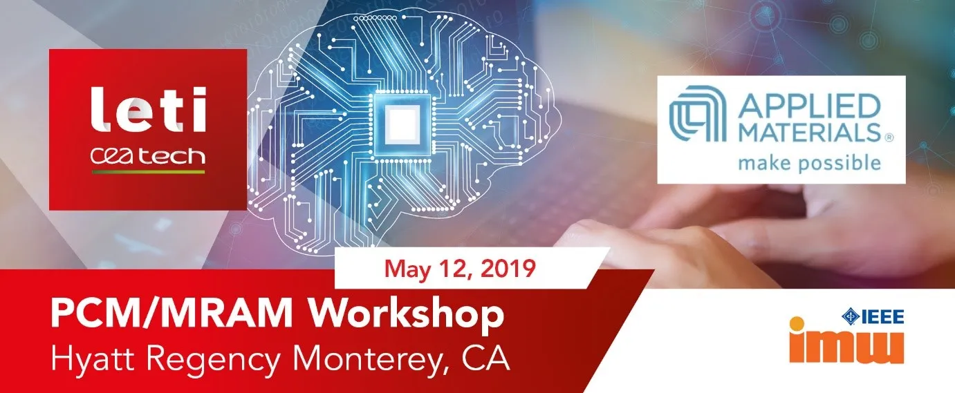
Two of the big, recent breakthroughs in memory technology – eMRAM and ePCM – have gotten their start in volume manufacturing on 28nm FD-SOI. In conjunction with the 2019 IEEE International Memory Workshop, SOI Consortium members Leti and Applied Materials have teamed up to give a technical program to explore short-term and long-term memory solutions. While the workshop is not specific to SOI, given the recent foundry announcements about ePCM and eMRAM for FD-SOI, the organizers predict it will be of particular interest to those following the greater SOI ecosystem. The event takes place at the end of the Sunday IMW tutorial day, starting at 5:30pm at the Hyatt Regency in Monterey, CA. Please see this page for the program and registration information. Here is the program: Emerging Non-Volatile Memory Promises Toward New Energy-Efficient Design and Applications - Michael Tchagaspanian, VP Business Development, CEA-Leti Technologies That Enable MRAM and PCRAM in Volume Manufacturing - Kevin Moraes, Vice President, Metal Deposition Products, Applied Materials Technology Improvements Directions of Emerging Non-Volatile Memory for New Applications Solutions - Etienne Nowak, Head of Memory Laboratory, CEA-Leti Integration Schemes and Challenges for New Memories in a New Artificial Intelligence Era -Michel Frei, Director, Advanced Product Technology Development, Applied Materials Jean-Eric Michallet, Head of Leti’s Microelectronics Components Department, Silicon Component Division is one of the organizers. Here is his overview: FD-SOI is expected to be a long-lived technology. It enables planar CMOS scaling and accommodates a great deal of More-than-Moore developments where its ability for low power and great analog performance can make a difference for IoT, Automotive, Machine Learning or 5G applications. But to do this it requires a high-performance and cost-effective non-volatile embedded memory option. The incumbent Flash cell is reaching the end of its roadmap due to the difficulty of shrinking the bitcell and manufacturing, as well as the finished wafer cost increase. Back-end integrated Random Access Memory in advanced CMOS process has been explored for many years now as a competitive solution for fast-write and low-voltage non-volatile embedded memories. Foundry availability of embedded Magnetic RAM and Phase Change RAM for FDSOI 28nm platforms has been announced recently, showing that these technologies have now reached industrial maturity. CEA-Leti and Applied Materials invite you to attend a technical program to explore short-term and long-term memory solutions, from early research to industrialization. Registration is open, free, and available to all IMW attendees, and others. However, as seating is limited and as we have already several participants pre-registered, registration is by invitation only and early registration is recommended. If you are interested, please email Jean-Eric Michallet. The event is presented in conjunction with the 2019 IEEE International Memory Workshop, to be held on Sunday, May 12th, 2019, Hyatt Regency, Monterey CA, starting at 5:30 pm.
Read More
Takeaway #1: As NXP VP Ron Martino noted in his opening keynote at the recent SOI Symposium in San Jose, FD-SOI is the technology platform for enabling edge computing, and ultra-low power is the sweet spot. Organized by the SOI Consortium with support from our members, the recent SOI Symposium in Silicon Valley was an enormous success. Close to 300 decision makers signed up – more than double what we saw just a couple years ago. Attendees spanned the ecosystem: from end-users to design to foundries and right up to the investment community. The presentations and panel discussions were absolutely terrific, and almost all are now freely available - click here to get them.The focus was heavily on FD-SOI this time, but some very interesting RF-SOI talks were given as well. This was a day packed with presentations by players from across the SOI ecosystem. In this post, we’ll only cover a few. But the others will follow quickly, so watch this page. And now without further ado, let’s dive in.NXP: In the Sweet SpotNXP VP Ron Martino presenting at the 2019 SOI Symposium in San Jose.NXP is designing FD-SOI into many new products, said Martino, GM of the i.MX Processor Application Product Line. There’s a new wave of products – generically you could call them IoT but in fact they’re found throughout the industry. It’s about interacting with the cloud, so edge processing is critical. His presentation, Embedded Processors for Future Applications, is now freely available for downloading from our website.The new i.MX7ULP is a great example of ULP in the sweet spot. From a design standpoint, it leverages IP, power optimization, and what he described as “starter biasing”. That gets them the long battery life with 2D 3D graphics they need for wearables and portables in consumer and industrial applications.NXP slide 10, SOI Symposium, San Jose '19 (Courtesy: NXP)Having deepened their expertise in biasing, NXP has now moved on to “advanced biasing” for the next generation of products. For example, the i.MX RT ULP (real-time, ultra-low-power) series are “cross-over” processors, which Martino says are the “new normal”. They deal with a high number of sensor inputs. The i.MX RT 1100 MCUs, which have been qualified for automotive and industrial applications, are breaking the gigahertz performance barrier with a low-power, 28nm FD-SOI process.Another new product leveraging advanced biasing is the i.MX RT 600. They’ve done hardware acceleration on specific functions and optimized around visionand voice integration at low cost and power.As shown at Embedded World '19, automotive app for NXP'x i.MX 8, which is on 28nm FD-SOI. (Courtesy: NXP)Likewise for the i.MX 8 and 8X subsystems for automotive and industrial applications. At Embedded World, they showed it driving advanced OLED screens, cameras (for parking, for example), V2X, audio, user monitoring (like driver pupil tracking), and integration into the windshield in a heads-up system. This is the high end of the capability of 28nm FD-SOI, he said. It’s a 6 CPU core system with multiple operating systems, about which he said: “It’s the dashboard...it’s amazing.”BTW, in another presentation, CoreAVI, which builds avionics, automotive and industrial products on NXP’s i.MX 8, addressed safety. You can get that here.FD-SOI enables a scalable solution for real-time and general compute with the lowest leakage memory, the best dynamic and static power, Martino concluded. NXP’s leadership in body biasing is enabling edge compute, and we can expect to see more content coming soon.In another NXP presentation later in the day, Stefano Pietri, Technical Director of the company’s Microcontrollers Analog Design Team caught a lot of people’s attention. A wave of cameras went up to capture each of his slides in Analog Techniques for Low Power, High Performance MPU in FD-SOI – but you can get the whole thing now from our website. It’s a very technical presentation, in which he details the many ways FD-SOI makes the analog team’s job easier, enabling them to get performance not available from bulk technologies. They developed a lot of in-house expertise and IP (see slide 16 for a catalog of the IP).Samsung: Enabling LP Endpoint ProductsTim Dry, Samsung Foundry Director of Edge Endpoint, SOI Symposium, San Jose '19Tim Dry, Director of Foundry Marketing: Edge and End Point presented Samsung’s FDS with MRAM: Enabling Today’s Innovative Low Power Endpoint Products. In a telling first, Samsung has made this presentation available on our website.FD-SOI covers the wide range of requirements for intelligent IoT, he explained: from high to low processing loads; and active to dormant processing duty cycles. That includes chips that will last for ten years, and need to be able to wake up fast and kick right into high performance. These products are 50% analog, and packaging is part of the solution (especially for the RF component).Samsung has been shipping 28nm FD-SOI (which they call 28FDS) since 2015, first in IoT/wearables, then in automotive/industrial and consumer. Yields are fully mature. In March 2019, they announced mass production of eMRAM on 28FDS. It’s a BEOL process, adding only 3 masks. It cuts chip-level power by 65% and RF power by 76% over 40nm bulk with external memory. Beyond the fact that it's 1000x faster than eFlash, eMRAM also has other advantages that make it especially good for over-the-air updates, for example.Samsung Foundry FD-SOI IP slide, SOI Symposium, San Jose '19 (Source: Samsung Foundry Keynote at SOI Symposium 2019, USA)Samsung also has RF and 5G mmWave products shipping in 28FDS. The company has a fantastic ecosystem of partners helping here, said Dry. In AI at the endpoint, they’re shipping IoT products for video surveillance cameras: some are high speed, but some are also low speed – it depends on the detection use case. And most importantly for the design ecosystem, the IP is all ready.Next up for Samsung is 18FDS, which will ship this year with RF, then in 2020 with eMRAM. 18FDS, Dry said, is optimized for power reduction. Compared to 28FDS, it’s got 55% lower power consumption, 25% less area and 17% better performance at the same power. You’ll hear more about it as well as their design services if you’re at the Samsung Foundry Forum in May (registration info here).ARM’s Biased ViewsKelvin Low, VP of Marketing for Arm’s Physical Design Group (PDG) gave a presentation entitled Biased Views on the Industry’s Broadest FDSOI Physical IP Solution. By way of background, Arm and Samsung Foundry recently announced a comprehensive, foundry-sponsored physical IP platform, including an eMRAM compiler for 18FDS. In case you missed it, at the time Arm Senior Product Marketing Manager Umang Doshi described the offering in an Arm Community / Developer physical IP blog, which Arm graciously agreed to share with ASN readers. Slide 9 from Arm's presentation, Silicon Valley SOI Symposium 2019.At the SOI Symposium, Low emphasized to the audience that Arm now has the broadest range of FD-SOI + IP solutions. It addresses mobile, consumer, IoT, automotive and AI/ML. There are 18FDS POP (processor optimized pipe) packages for Arm Cortex-A55, Cortex-R52 and Cortex-M33 processors. IP integrates biasing and a number of standard PVTs (corners). And since the Samsung platform is foundry-sponsored, it’s free.Slides 6 and 11 from Arm's presentation, Silicon Valley SOI Symposium 2019. The goal of POP IP is to enable partners to implement and tapeout Arm cores with the fastest turn-around time and best-in-class PPA while maximizing the benefits of process technology.Arm did a test chip with eMRAM, which they’ve just gotten back. It’s functional (some details are available in slide 14 of their presentation), and the company is now preparing a demo board that they’ll be showing shortly. Watch this page!That's all for this post. The next post -- part 2, covering presentations by Synaptics, GlobalFoundries, STMicroelectronics, Dolphin Integration and Anokiwave -- is now available. Click here to read on.
Read More
FD-SOI for RF and mmWave communications is a hot topic. In high-data rate communications like RF and millimeter-wave devices in particular, FD-SOI delivers high-performance with numerous unique advantages, making it most likely the fastest RF-CMOS technology on the market. If you’d like to take a deep dive and learn more about it, Soitec and Incize are sponsoring a free, full-day workshop in Grenoble on April 4th, 2019. Click here for registration information. The workshop follows the day after the IEEE/EDS EuroSOI-ULIS conference there (you can read about the full conference in a previous ASN post). This technical workshop will cover the FD-SOI technology platform with a focus on its compatibility with RF mmWave communications. Attendees will hear from notable FD-SOI leaders and experts from leading industry and research institutions presenting updates on key developments and building blocks across the semiconductor value chain. Topics will include circuit design, device fundamentals, simulation and characterization of RF devices, test, CMOS technology and substrate technologies enabling FD-SOI. In addition, the workshop will include an overview about how FD-SOI technology is benefiting current and future end user applications. Here’s the agenda: [caption id="attachment_15990" align="alignleft" width="945"] FD-SOI technology platform: new standards for emerging consumer electronics [Click to enlarge.][/caption]
Read More
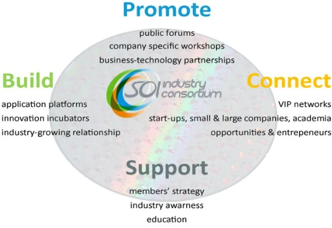
Welcome to our first post for 2019 here at the SOI Consortium's Advanced Substrate News. First and foremost, may we wish you and yours a safe, happy, healthy and prosperous year. It should be a good year across the SOI ecosystem, with new products, players, IP, technologies and tools -- and high volumes. What's new? Let's start with the people, as the Consortium welcomes new team members. Jon Cheek of NXP will join Carlos Mazure as Executive Co-Director. He'll be replacing ST's Giorgio Cesana in that role – and goodness knows those are some big shoes to fill. Giorgio has given of his time and expertise so tirelessly over many years. He'll of course still be a key resource for the SOI ecosystem, and though we'll miss him here at the Consortium, we know he'll be doing great things in SOI at ST. So a heartfelt thanks to Giorgio Cesana from all of us. Jon Cheek has a long history in engineering management at companies that have been leading users of SOI: AMD, Freescale and now NXP. As such, he understands what companies need to design great products, and how the Consortium can help further build, promote, connect and support the ecosystem. The Consortium team also welcomes Jean-Eric Michallet of Leti, who'll bring deep bizdev expertise and a keen sense of what it takes to reach further into the ecosystem. (Astute long-time ASN readers might remember his post from five years ago about 3D monolithic integration – now dubbed “Cool Cube” by Leti.) And finally, look to hear more from and about the Consortium, as our team is rounded out with the addition of the comm marketing savvy of Erin Berard of Soitec. In addition to new team members, the Consortium is very pleased to welcome new member Applied Materials. Though new to the Consortium, AMAT has a long history in the heart of SOI ecosystem – in fact they've been working with SOI wafer-leader Soitec for over 25 years. AMAT ion implanters are a key enabler to what became and is Soitec's industry-leading Smart CutTM SOI wafer manufacturing process. And of course AMAT equipment is used to make virtually every chip in the world, so their breadth of vision as a consortium member is clearly a fabulous addition. 2019 will also be marked by the expansion of the highly successful SOI Academy series, the first of which was held this past fall in Shanghai. We'll keep you posted as these and other Consortium events are announced throughout the year. In fact, 2019 marks a decade of (excellent!) SOI Consortium events events around the world: our first symposium was held back in 2009. Kicking off this year, save April 9th on your calendar for our Annual SOI Silicon Valley Symposium. Then watch this page for more events across the globe. What will the year bring? On the product side, RF-SOI for 5G is of course super hot. Last summer, a SemiconductorEngineering headline proclaimed RF-SOI Wars Begin. And what we heard at the International RF-SOI Workshop last fall in Shanghai (presentations here) certainly confirmed that in the coming year the race will continue unabated. [caption id="attachment_14476" align="alignright" width="300"] Part 3 in SemiconductorEngineering's "Experts at the Table" series on FD-SOI featured James Lamb of Brewer Science, Giorgio Cesana of ST, Olivier Vatel of Screen, and Carlos Mazure of Soitec. (Image courtesy: SemiconductorEngineering.com)[/caption] And for FD-SOI, you might want to read the SE series published over the last six months. The latest, published a couple of weeks ago looks at FD-SOI at the Edge. There are some great insights from SOI Consortium members there. In terms of products, too, there's lots of activity. Last summer, Samsung indicated they'd taped out over 60 products since they first began offering 28FDS three years ago. It's a trend they see accelerating. Full production of 18FDS is slated for this fall. And also last summer GlobalFoundries indicated they had over 50 client designs on 22FDX. “We’re only just beginning,” said GF CEO Tom Caulfield at the time. “We have found a way to separate ourselves from the pack by emphasizing our differentiated FD-SOI roadmap and client-focused offerings that are poised to enable connected intelligence. " For its part, ST, as we learned at the last SOI Consortium Japan Workshop, has been doing FD-SOI for five years now. And while we don't have number, we learned that some of those products are now in their second and third generations, and that some big FD-SOI chips coming out this year with embedded memory and RF, with especially good traction in mmWave, automotive and IoT. So while the outlook for the overall industry is anyone's guess for the coming year, the outlook for chips built on SOI technologies is very good indeed.
Read More
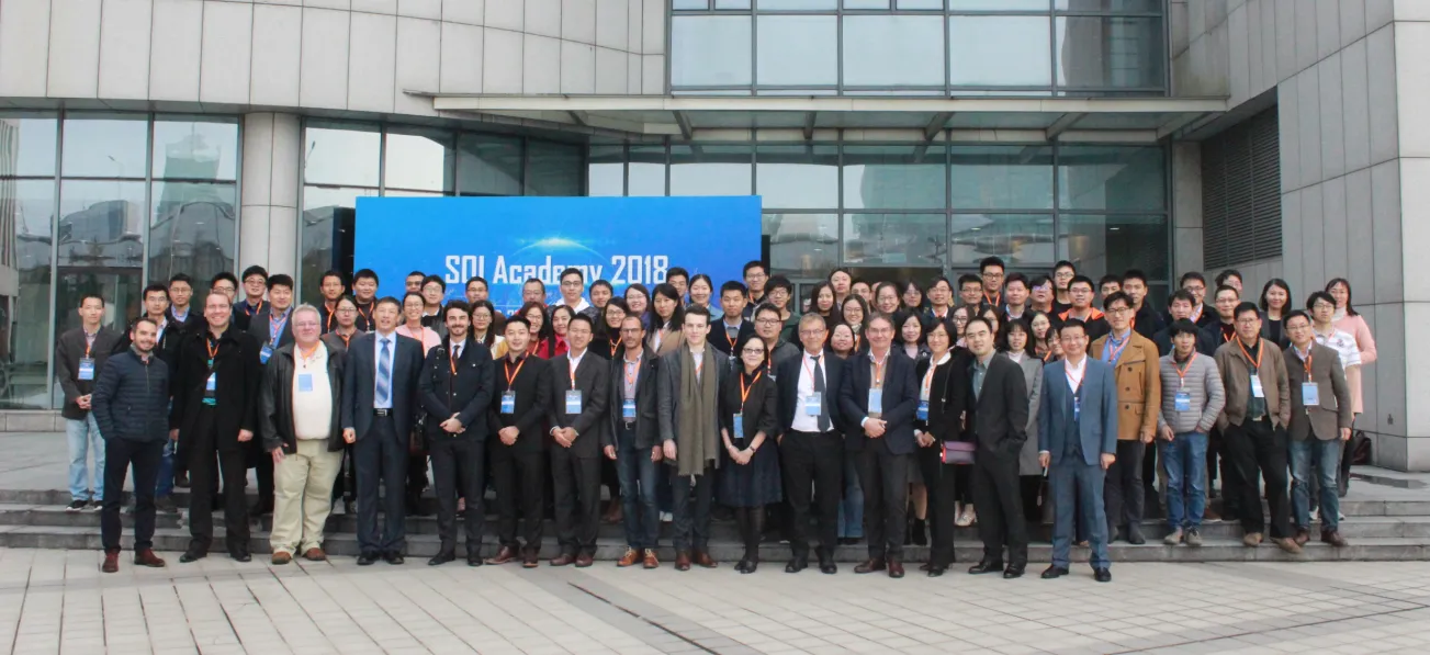
There were over 220 participants at the recent SOI Academy FD-SOI Training event organized in Shanghai. The event extended over two days, with the first day covering a basic introduction to the technology as well as the ecosystem worldwide and in China. The second day was hands-on professional training. Attendees got a comprehensive understanding of how to leverage the benefits and flexibility of FD-SOI design techniques for low-power chips including logic, mixed-signal/RF and analog blocks. They had a great line-up of experts from whom to learn – check out the agenda here. There was also a follow-up press release (in Chinese) from SITRI here. There will be more of these SOI Academy events in cities across China in the year to come – we'll keep you posted (and of course, keep checking back for news on the Consortium's Events page). [caption id="attachment_12981" align="aligncenter" width="1000"] SOI Academy '18 keynotes by: Dr. Mark Ding, CEO, SITRI; Dr. Carlos Mazure, EVP Soitec and Chairman/Executive Director SOI Consortium. Dr. Julien Arcamone, EVP Leti. (Images courtesy: SITRI). Lower right: the hands-on FD-SOI training.[/caption] The two-day seminar and hands-on FD-SOI design training was (superbly!) co-organized by SITRI and Leti, with the support of the SOI Industry Consortium at the Jiading SIMIT campus outside of Shanghai. Just to put this in perspective, SIMIT and SITRI are absolutely key players in China's chip ecosystem. SIMIT is the Shanghai Institute of Microsystem and Information Technology, one of the most venerable institutes in the Chinese Academy of Science (CAS) and one of the world's earliest pioneers in SOI. SITRI is the Shanghai Industrial μTechnology Research Institute, an international innovation center focused on globally accelerating innovation and commercialization of More-than-Moore for IoT. Both institutions are under the aegis of Dr. Xi Wang, Chairman of SITRI, Director General of SIMIT, Academician of CAS, and champion of all things SOI in China. At this Shanghai event, the participants came from industry (including big companies, SMEs and startups) and technical institutions. In fact as well as attendees from Shanghai people voyaged from other cities such as Shenzhen and Chengdu. The designers participating to the FD-SOI training day were all experienced in design and highly motivated in learning FD-SOI design, notes Carlos Mazure, Chairman Executive Director of the SOI Industry Consortium, and Executive VP of Soitec. “This made it possible to dive into the specificities of FD-SOI,” he said, adding that, “The focus on RF was very timely.” Day 1: Intro to FD-SOI The first afternoon opening keynotes were made by SITRI CEO Dr. Mark Ding and Leti EVP Dr. Julien Arcamone. These were followed by overview talks by execs from Soitec, Verisilicon and GlobalFoundries. After a lively networking break, three talks delved into FD-SOI technology. The first was by Professor Sorin Cristoloveanu, Laureate of the IEEE Andrew Grove Award and Director at the CNRS (the French National Center for Scientific Research – the largest governmental research organization in France and the largest fundamental science agency in Europe). He covered device physics and characterization techniques. This was followed by talks on the technology by Soitec Fellow Bich-Yen Nguygen, and by Dr. Christophe Tretz, IBM Sr. Engineer on product design methodology. The day ended with a dinner, where Professor Cristoloveanu says enthusiastic technical discussions continued unabated (and continued even further in follow-up emails), lots of business cards were exchanged, and opportunities for further education were explored. Day 2: Hands-on Training The second day, designers got hands-on training from Leti experts using FD-SOI PDKs, first in the morning on digital, then in the afternoon on RF. Everyone loved the lively discussion and in-depth exchanges between the experts and the designers. They agreed that FD-SOI has important applications and differentiated competitive advantages for IoT, 5G, automotive, AI and other fields. At the end of the training, Leti and SITRI jointly issued SOI Academy certificates of completion to the designers. Feedback from participants was very good. Some asked for further education and for hands-on testimonials from companies that are already designing and manufacturing products on FD-SOI. “The participants were focused, motivated, involved, with good knowledge, which helped make the three hours of Digital training effective,” said Dr. Alexandre Valentian, Leti Sr. Expert, Digital Design. “The IT team was very helpful in setting up the training, the students accounts and the hardware infrastructure.” “The training on Basics of FD-SOI RF circuit was a great success thanks to the efficiency of our Chinese partners and also thanks to the enthusiasm and the good level of our trainees. As senior Expert of CEA Leti I was really impressed by the professionalism of the organization team. For all these reasons, I’m very glad to have had the opportunity to contribute to the 2018 SOI Academy,” said Dr. Baudouin Martineau, Leti Sr. Expert, RFIC Design Technologies. “The professionalism, efficiency and enthusiasm of our Chinese partners and the level and technical relevance of all trainees made the training on Basics of FD-SOI RF circuit a great success and fruitful experience,” added Frédéric Hameau, Sr. RF Research Engineer, Leti Project Leader, Architecture, IC Design Embedded Software Division, RF Architectures and ICs Laboratory. “It was a pleasure to get the opportunity to be part of this first edition of SOI academy 2018.” The organizers would like to thank the sponsors, including: the SOI Consortium and its members Soitec, VeriSilicon, GlobalFoundries, Simgui and Cadence, as well as Mentor, ProPlus and other companies and institutions in China and worldwide. Dr. Mazure notes that special recognition must go to Dr. Julien Arcamone, EVP, Leti-CEA and to Qing Wang-Bousquet, SITRI representative, for the perfect and smooth organization, and to the Leti instructors, who are international experts and highly committed. “As one of the main initiators and organizers of the 2018 SOI Academy, I wanted to personally thank all of you for your respective contribution to this first edition of the SOI Academy,” concludes Dr. Arcamone. “Undoubtedly, it was a great success, very well organized and fluid and we can be proud of that.”
Read More
The presentations from the SOI Consortium sponsored workshop held during Semicon West are now posted and freely available on the website – click here to see the full agenda with links to the presentations. The workshop, entitled 4G/5G Connectivity: Opportunities for the SOI Supply Chain, was well-attended and generated excellent discussions. If you don't have time to look at all of the ppts, here are quick overviews. Market Overview and FD SOI Opportunities, by Handel Jones, CEO, IBS. Handel Jones is an industry veteran, China expert and longtime follower of the SOI ecosystem. High performance with low power consumption are the key requirements for the continued growth in the semiconductor industry, he said, making FD-SOI the right choice for a wide range of products. Here's how he sees it: [caption id="attachment_12312" align="alignleft" width="300"] (Courtesy: IBS and SOI Consortium)[/caption] He estimates the yearly TAM (total available market) for FD-SOI based products in the range of $46 billion over the next 10 years, largely driven by needs for ultra-low power and RF integration. He goes on to break out volumes by applications (including ISPs – image signal processors; and CIS – CMOS image sensors), foundry markets by feature dimension and to map out technology trends. Mobile Radio Transformation in the Age of 5G: A Perspective on Opportunities for SOI, Peter Rabbeni, Vice President, Globalfoundries. Peter Rabbeni is an RF expert par excellence, having overseen the shipping of over 35 billion RF-SOI products to date. In his presentation, he details how 5G NR (New Radio) sub-6GHz frequency band specifications significantly increase frequency range and channel bandwidth, and how new band support and MIMO complexity and die size per handset are driving complexity in RF FEMs. Furthermore, 5G/mmWave phased arrays are driving a paradigm shift in the approaches that can be taken, he explains, so greater integration is needed. Here's a great slide showing where GF's two main SOI technologies come into play: [caption id="attachment_12311" align="alignleft" width="1000"] (Courtesy: GlobalFoundries and SOI Consortium)[/caption] Empowerment of 5G with SOI-Based Technologies, Emmanuel Sabonnadière, CEO, Leti-CEA. [caption id="attachment_12310" align="alignleft" width="300"] (Courtesy: Leti and SOI Consortium)[/caption] Working in partnership with industry leaders around the world, Leti has been the research powerhouse behind all things SOI since the early 1980s. In fact Reuters ranks them #2 in their most recent list of the World’s Most Innovative Research Institutions. This presentation reviews the key technical benefits of FD-SOI for IoT and IMT (that's international mobile communications, btw). Engineered Substrates – at the Foundation of 5G, Thomas Piliszczuk, Executive Vice President, Soitec. This presentation really puts the context around engineered substrates. Here are two excellent and useful slides here that identify which engineered substrates go where in the 5G world, and the engineered substrates that Soitec provides. Check these out: [caption id="attachment_12309" align="alignleft" width="1000"] (Courtesy: Soitec and SOI Consortium)[/caption] [caption id="attachment_12308" align="alignleft" width="1000"] (Courtesy: Soitec and SOI Consortium)[/caption] Ultra-thin Double Layer Metrology with High Lateral Resolution, Bernd Srocka, Vice President, Unity GmbH. [caption id="attachment_12307" align="alignleft" width="300"] (Courtesy: Unity and SOI Consortium)[/caption] In case you're not familiar with them, Unity provides a wide range of solutions in metrology and inspection. Both the top silicon layer and BOX layer of wafers for FD-SOI applications have draconian requirements that have required new approaches in metrology to ensure the thickness and homegeneity control of these very thin layers. China 5G Plan and SOI Ecosystem, Jeffrey Wang, CEO, Simgui. Shanghai-based Simgui partners with Soitec, using SmartCut™ technology for the production of RF-SOI wafers. It is doubling its capacity to reach 400K over the next year, and expanding into 300mm. China is aggressively working on 5G and plans to deploy 5G commercialization in 2020. Jeff Wang's is a terrific presentation detailing the rollout. (BTW, in addition to the massive funding effort underway, the government created the National Silicon Industry Group (NSIG) to support the semiconductor material ecosystem in China. You'll want to keep up with what's going on here). Here's the slide that summarizes the SOI ecosystem in China – the presentation then goes on to detail who does what. [caption id="attachment_12306" align="alignleft" width="1000"] (Courtesy: Simgui and SOI Consortium)[/caption] Inspection and Metrology Relevance in SOI Manufacturing, Jijen Vazhaeparambil, Vice President General Manager, KLA-Tencor. [caption id="attachment_12305" align="alignleft" width="300"] (Courtesy: KLA-Tencor and SOI Consortium)[/caption] K-T has played a strategic role in the SOI story going back for decades (and in fact they wrote a piece for the third edition of ASN back in 2005!), ensuring metrology innovations for things that hadn't previously need detection and measurement. With each new set of requirements, they rose to the occasion with wafer metrology solutions that helped increase quality and decrease costs. This presentation recaps some of them.
Read More
Leti and Soitec have announced a new collaboration and five-year partnership agreement to drive the R D of advanced engineered substrates, including SOI and beyond. This agreement brings the traditional Leti-Soitec partnership to a whole new dimension and includes the launch of a world-class prototyping hub associating equipment partners to pioneer with new materials, The Substrate Innovation Center will feature access to shared Leti-Soitec expertise around a focused pilot line. Key benefits for partners include access to early exploratory sampling and prototyping, collaborative analysis, and early learning at the substrate level, eventually leading to streamlined product viability and roadmap planning at the system level. [caption id="attachment_12066" align="aligncenter" width="644"] CEOs Emmanuel Sabonnadière (Leti) and Paul Boudre (Soitec) announcing the new Substrate Innovation Center during Semicon West '18. (Image courtesy: Leti)[/caption] Leading chip makers and foundries worldwide use Soitec products to manufacture chips for consumer applications targeting performance, connectivity, and efficiency with extremely low energy consumption. Applications include smart phones, data centers, automotive, imagers, and medical and industrial equipment, but this list is always growing, along with the need for flexibility to explore new applications starting at the substrate level. At the Substrate Innovation Center, located on Leti’s campus, Leti and Soitec engineers will explore and develop innovative substrate features, expanding to new fields and applications with a special focus on 4G/5G connectivity, artificial intelligence, sensors and display, automotive, photonics, and edge computing. “Material innovation and substrate engineering make entire new horizons possible. The Substrate Innovation Center will unleash the power of substrate R D collaboration beyond the typical product road maps, beyond the typical constraints,” said Paul Boudre, Soitec CEO. “The Substrate Innovation Center is a one-of-a-kind opportunity open to all industry partners within the semiconductor value chain.” Whereas a typical manufacturing facility has limited flexibility to try new solutions and cannot afford to take risks with prototyping, the mission of the Substrate Innovation Center is to become the world’s preferred hub for evaluating and designing engineered substrate solutions to address the future needs of the industry, inclusive of all the key players, from compound suppliers to product designers. Using state of the art, quality-controlled clean room facilities, and the latest industry-grade equipment and materials, Leti and Soitec engineers will conduct testing and evaluation at all levels of advanced substrate R D. “Leti and Soitec’s collaboration on SOI and differentiated materials, which extends back to Soitec’s launch in 1992, has produced innovative technologies that are vital to a wide range of consumer and industrial products and components,” said Emmanuel Sabonnadière, Leti CEO. “This new common hub at Leti’s campus marks the next step in this ongoing partnership. By jointly working with foundries, fabless, and system companies, we provide our partners with a strong edge for their future products."
Read More
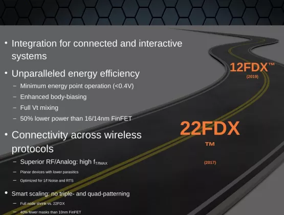
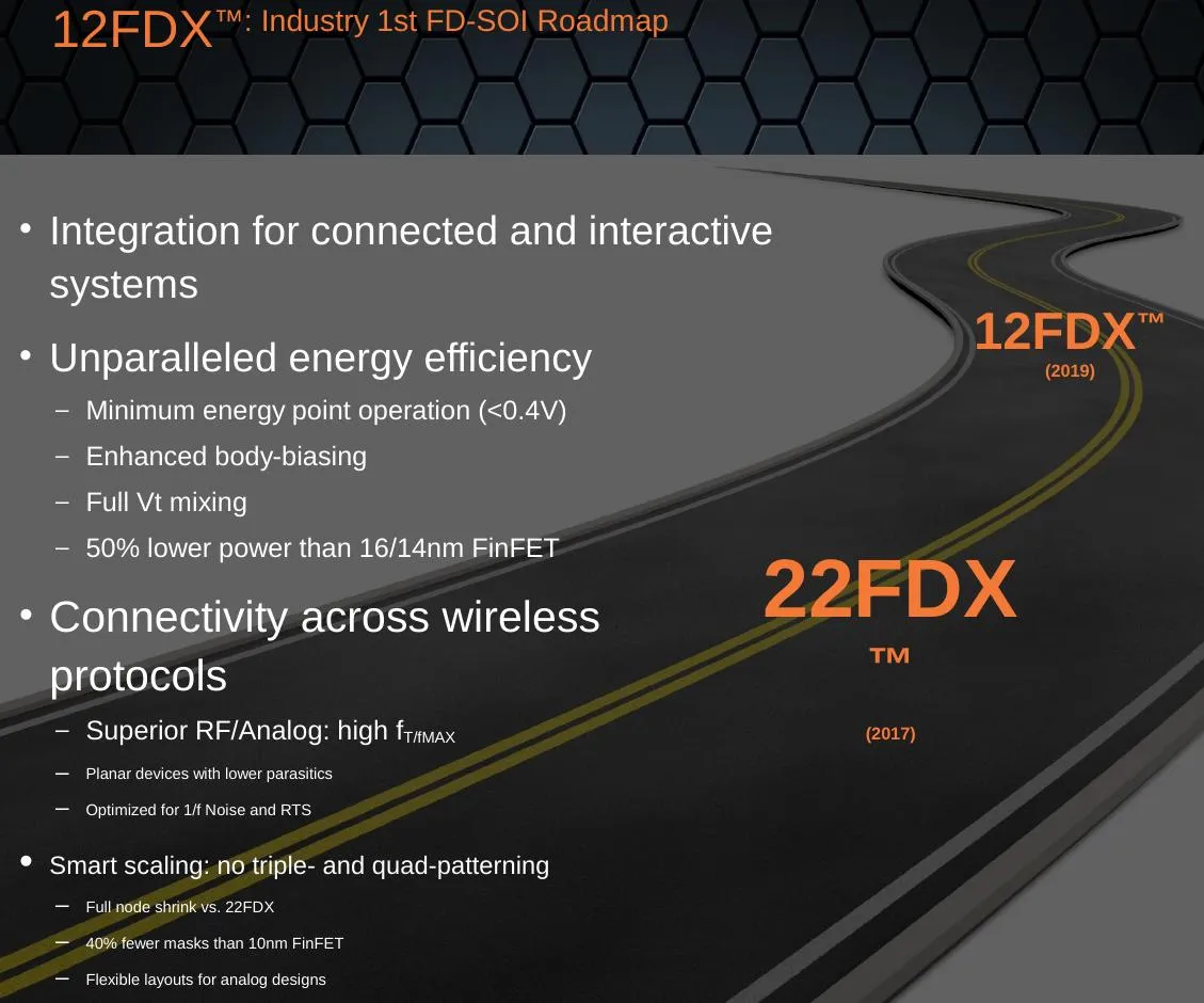
12nm FD-SOI has now officially joined the GlobalFoundries’ roadmap, targeting intelligent, connected systems and beating 14/16nm FinFET on performance, power consumption (by 50%!) and cost (see press release here). Customer product tape-outs are expected to begin in the first half of 2019. GloFo also announced FDXcelerator™, an ecosystem designed to give 22FDX™ SoC design a boost and reduce time-to-market for its customers (press release here). [caption id="attachment_9874" align="aligncenter" width="610"] (Courtesy: GlobalFoundries and SOI Consortium Shanghai FD-SOI Forum 2016)[/caption] The news turned heads worldwide (hundreds of publications immediately picked up the news) – and especially in China. "We are excited about the GlobalFoundries 12FDX offering and the value it can provide to customers in China," said Dr. Xi Wang, Director General, Academician of Chinese Academy of Sciences, Shanghai Institute of Microsystem and Information Technology. “Extending the FD-SOI roadmap will enable customers in markets such as mobile, IoT, and automotive to leverage the power efficiency and performance benefits of the FDX technologies to create competitive products." Wayne Dai, CEO of VeriSilicon (headquartered in Shanghai but designing for the world’s biggest names in the chip biz), added, “We look forward to extending our collaboration with GlobalFoundries on their 12FDX offering and providing high-quality, low-power and cost-effective solutions to our customers for the China market. The unique benefits of FD-SOI technologies enable us to differentiate in the automotive, IoT, mobility, and consumer market segments.” The ultra-thin FD-SOI wafers are where it all starts, and they’re ready to go in high volume, says Paul Boudre, CEO of SOI wafer leader Soitec. “We are very pleased to see a strong momentum and a very solid adoption from fabless customers in 22FDX offering,” he adds. “Now this new 12FDX offering will further expand FD-SOI market adoption. This is an amazing opportunity for our industry just in time to support a big wave of new mobile and connected applications.” All About 12GloFo’s 12FDXTM platform, which builds on the success of its 22FDXTM offering, is designed to enable the intelligent systems of tomorrow across a range of applications, from mobile computing and 5G connectivity to artificial intelligence and autonomous vehicles. Increased integration of intelligent components including wireless (RF) connectivity, non-volatile memory, and power management—all while driving ultra-low power consumption—are key 12FDX selling points that FinFETs can’t touch. The technology also provides the industry’s widest range of dynamic voltage scaling and unmatched design flexibility via software-controlled transistors—capable of delivering peak performance when and where it is needed, while balancing static and dynamic power for the ultimate in energy efficiency. [caption id="attachment_9873" align="aligncenter" width="610"] (Courtesy: GlobalFoundries and SOI Consortium Shanghai FD-SOI Forum 2016)[/caption] “Some applications require the unsurpassed performance of FinFET transistors, but the vast majority of connected devices need high levels of integration and more flexibility for performance and power consumption, at costs FinFET cannot achieve,” said GLOBALFOUNDRIES CEO Sanjay Jha. “Our 22FDX and 12FDX technologies fill a gap in the industry’s roadmap by providing an alternative path for the next generation of connected intelligent systems. And with our FDX platforms, the cost of design is significantly lower, reopening the door for advanced node migration and spurring increased innovation across the ecosystem.” Kudos came in from G. Dan Hutcheson, CEO of VLSI Research, IBS CEO Handel Jones, Linley Group Founder Linley Gwennap, Dasaradha Gude, CEO of IP/design specialists INVECAS, Leti CEO Marie Semeria and NXP VP Ron Martino (they’ve already started on 28nm FD-SOI for their i.MX line – read his superb explanations in ASN here). 22 Design Plug ‘n PlaySimultaneously to the 12FDX announcement, GloFo announced the FDXcelerator Partner Program. It creates an open framework under which selected Partners can integrate their products or services into a validated, plug and play catalog of design solutions. This level of integration allows customers to create high performance designs while minimizing development costs through access to a broad set of quality offerings, specific to 22FDX technology. The Partner ecosystem positions members and customers to take advantage of the broad adoption and accelerating growth of the FDX market.Initial partners of the FDXcelerator Partner Program are: Synopsys (EDA), Cadence (EDA), INVECAS (IP and Design Solutions), VeriSilicon (ASIC), CEA Leti (services), Dreamchip (reference solutions) and Encore Semi (services). These companies have already initiated work to deliver advanced 22FDX SoC solutions and services. Initial FDXcelerator Partners have committed a set of key offerings to the program, including: tools (EDA) that complement industry leading design flows by adding specific modules to easily leverage FDSOI body-bias differentiated features, a comprehensive library of design elements (IP), including foundation IP, interfaces and complex IP to enable foundry customers to start their designs from validated IP elements, platforms (ASIC), which allow a customer to build a complete ASIC offering on 22FDX, reference solutions (reference designs, system IP), whereby the Partner brings system level expertise in Emerging application areas, enabling customers to speed-up time to market, resources (design consultation, services), whereby Partners have trained dedicated resources to support 22FDX technology; and product packaging and test (OSAT) solutions. Additional FDXcelerator members will be announced in the following months.
Read More