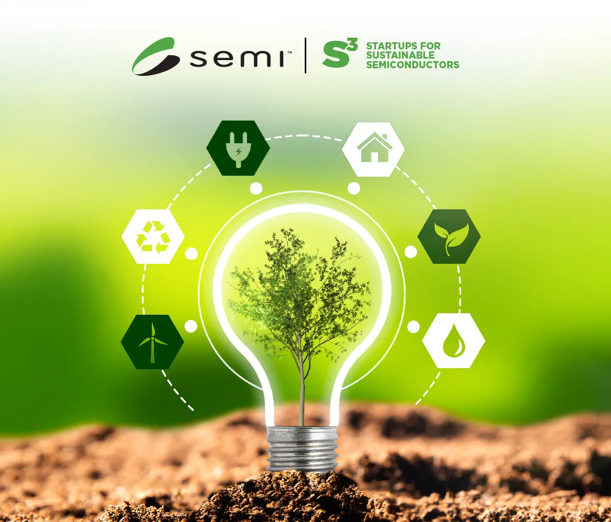
The SEMI Startups for Sustainable Semiconductors (S3) program, now in its 5th year of inviting startups to apply, is pleased to announce the 33 startups chosen to move to the semifinalist virtual pitch event happening July 29-30. From this pool, 10-12 finalists will be selected and invited to pitch to a live audience at SEMICON West 2026 in San Francisco, October 13-15, 2026. The committee, made up of experienced Corporate Venture Capitalists (CVCs) from the global semiconductor industry, received impressive submissions in all four categories for 2026:Decarbonized Semiconductor ManufacturingDesign for Sustainability – Chips PackagingDatacenter Efficiency in Power Delivery and ThermalsNew Frontiers in Sustainable ComputingLed by Micron this year, the program’s strongest feature is the exposure to the CVCs, as well as the personal mentoring each semifinalist receives. The mentoring topics are tailor-made to align with the greatest need of the startup and can range from a basic introduction to semiconductor manufacturing, to connecting them to funding sources. A full analysis of the program kicked off this year’s efforts and is captured in a report available here.The program saw an increase in quality applications with a geographically diverse group of semifinalists who will all share their solutions for the building and use of more sustainable electronics. Are you an investor and would like to receive notice of the virtual and live pitch events around S3? Register your interest here. 2026 S3 SemifinalistsAikido TechnologiesSan Francisco, CA, USAAikido Technologies is building clean, marine datacenters - AI-grade compute on the ocean, built faster, cheaper and more efficiently than conventional infrastructure. Axonal NetworksMontreal, QC, CanadaAxonal Networks develops digital photonics technology (paraLITE™) that performs computation directly in silicon photonics. Our devices eliminate electronic bottlenecks, enabling ultra-high-speed, energy-efficient computing for AI infrastructure and next-generation semiconductor systems. C1 BioChicago, IL, USAC1 Bio is building a biomanufacturing platform that converts low-cost agricultural waste into high-performance photoresist materials for semiconductor manufacturing. Our initial product, bio-based 4-acetoxystyrene (ASM), is a drop-in replacement for petroleum-derived monomers, enabling sustainable, domestic production of critical lithography materials without compromising cost, purity, or performance. CHIPADD, Corp.Binghamton, NY, USACHIPADD is the first to additively manufacture ultra-efficient copper cooling features directly onto the surface of GPU, CPU, and other high power silicon chips. The company’s innovation includes materials and methods for robust bonding, manufacturing of solid and porous cooling features, enhanced materials for cooling, manifold and precision jet design. EMTAR Technologies IncRichmond, VA, USAEMTAR Technologies designs highly integrated beamforming SoCs and RF front-end ICs for 6G non-terrestrial networks. Our chips enable low-latency, high-throughput satellite communications while reducing power consumption and hardware complexity, improving energy efficiency of satellite communication infrastructure. enaDyneLeipzig, Saxony, GermanyenaDyne builds a fully electric, modular abatement system for semiconductor fabs based on non-thermal plasma catalysis. Our reactor destroys PFCs, VOCs, and NOx at 99% DRE through electron-impact chemistry at near-ambient temperature, fitting the same footprint as burn-wet for direct drop-in replacement. Same hardware extends to electrified chemical synthesis. FlexcomputeBoston, MA, USAFlexcompute builds a GPU-native physics simulation platform: Tidy3D (photonic/electromagnetic FDTD), PhotonForge (photonic design automation), Flexcompute RF (full-wave EM), and Flow360 (CFD/thermal), delivering results 50-500x faster than legacy CPU tools. FlexAgent, our AI assistant, enables engineers to run and iterate simulations via natural language, accelerating chip and data center component design. Floadia CorporationTokyo, JapanAI data centers are consuming large power. This is a global issue. Floadia developed analog CiM (Computing in Memory) technology that execute AI matrix calculation at 1/1000 power of digital way to solve AI data centers power issue using unique memory technology. FS2Saint Louis, MO, USAFS2 is developing a revolutionary Monolithic 3D (M3D) integration platform and memory. We are building next-generation stacked 3D SRAM and Process-on-Memory (POM) architectures. Our product delivers memory solutions with superior bandwidth, capacity, low latency, high energy efficiency, and lost cost for AI workloads. HEXAspec IncHouston, TX, USAHEXAspec develops advanced molding compounds for semiconductor encapsulation using high-aspect-ratio hexagonal boron nitride (hBN) nanosheets in polymers. Its scalable, patent-protected exfoliation process enables 10x — higher thermal conductivity while maintaining electrical insulation, mechanical strength, and compatibility with standard OSAT and foundry packaging for HPC, automotive, and edge-AI applications. IL-BSC TechnologiesBrooklyn, NY, USAHelium-free wafer thermal stabilization system for electrostatic chuck applications. Replaces helium backside cooling with low-vapor-pressure ionic liquid thermal fluid, tier-specific chemical getter, dual-mode acoustic purge, and plasma-resistant barrier integrity sensor. Eliminates dependence on critical helium supply while maintaining thermal uniformity required for advanced node semiconductor manufacturing. IWI Australia Pty LimitedSydney, NSW, AustraliaWe have developed and piloted a patent-pending catalytic quench of hydrogen peroxide (CQ) in fab wastewater, especially in complex water matrix with high peroxide load, extreme acidity and heavy metal. We have also developed a patent-pending oxidation process for triazole, another pain-point of fab operation and water reuse. K1 SemiconductorChicago, IL, USAAt K1 Semiconductor, we create engineered semiconductor wafers by peeling thin layers from high-quality single-crystal “parent” wafers. Our patented wafer splitting method releases a 5-50 micron-thick layer of single-crystal material from the parent wafer, which is then transferred and bonded to a handle wafer to create a custom semiconductor wafer. KoolMicro, Inc. Dongtan, Gyeonggi-do, South KoreaKoolMicro is engineering the "Thermal Highway" for the AI era. We develop Integrated Manifold MicroChannel (IMMC) modules that handle 4,000W+ thermal loads. Our Direct-to-Chip solution utilizes vertically sprayed coolant to remove heat directly from the chip level, ensuring next-gen GPUs and CPUs never throttle. NanoPattern Technologies, inc.Chicago, IL, USAAt NanoPattern, we are commercializing a photodefinable hardmask (PDH) liquid formulation for advanced semiconductor packaging. Our resin-free, sustainable, metal-oxide formulation enables the use of non-photosensitive polymer dielectrics to form sub-micron lines and vias for high-resolution RDLs. We eliminate expensive vacuum deposition tools, drastically improving design freedom for next-generation AI chips. NicslabRochester, NY, USANicslab develops advanced electronic and photonic control systems that enable precise testing, operation, and deployment of photonic integrated circuits and semiconductor devices. Its platforms replace complex lab equipment with scalable, software-driven solutions, helping transform photonics from research into reliable, real-world applications across AI, data centers, quantum technologies, and advanced sensing. NordAmpsLund, Skåne County, SwedenNordAmps develops ultra‑high‑performance RF circuits using vertical III‑V nanowire transistors on standard silicon. The architecture delivers higher frequency performance, lower power use and smaller footprint than GaAs, GaN or SiGe, while being fully compatible with existing semiconductor fabs for true scalability. Normal ComputingNew York, NY, USANormal EDA is a purpose-built AI platform for semiconductor design that applies auto-formalization, combining LLMs with formal logic, to accelerate chip design and prove correctness. Deployed with half of the top ten semiconductor companies by revenue, and used to design our silicon: CN101, the world's first thermodynamic computing chip. NSS WaterGothenburg, Västra Götaland County, SwedenAt NSS water we are building a solution to drastically decrease water and chemical use in semiconductor industry and doing advanced solvent reclaim of downstream waste from rinse processes such as wafer cleaning, etch and more. With our new patent technology we can do IPA-reclaim and produce extremely pure water Plaid SemiconductorsAtlanta, GA, USAPlaid is building a modular platform that enables rack-on-package integrating large numbers of AI processors onto a single package. By collapsing distance within systems, we deliver higher bandwidth, lower power loss, and dramatically improved performance for next-generation AI infrastructure. Power to HydrogenColumbus, OH, USAPower to Hydrogen is building industrial-scale AEM electrolysers that reduce the stack costs by 65% for clean hydrogen production. For semiconductor manufacturing, we are developing a pathway from a 10 kW pilot to a 500 kW fab-ready module for onsite, ultra-high purity, low-carbon hydrogen production. Powerlattice Technologies Inc.Phoenix, AZ, USAThe first true monolithic integrated voltage regulator designed for high wattage ( 1kw) ASICs and XPUs. Project LegacyLondon, England, United KingdomA neuromorphic semiconductor for autonomous systems (robotics). Our chip architecture consists of neurons taken from the 7-brain regions within neuroscience. This will allow for predictive learning and tasks to occur once a software algorithmic layer is applied. We see current neuromorphic hardware layers as the problem. Rise Technology srlMilano, Lombardy, ItalyRiseTech develops next-generation semiconductor equipment based on its proprietary Dynamic Drop™ technology, overcoming the limits of conventional electroplating. The platform enables high-uniformity, high-throughput formation of interconnects, improving yield and enabling advanced architectures in heterogeneous integration, including chiplets, DRAM stacking, and 2.5D/3D packaging. SolidT Technologies LtdPetach Tikva, Central District, IsraelSolidT develops thin-film thermoelectric solutions enabling localized, active thermal control in semiconductor systems. Our technology mitigates hotspots, reduces thermal gradients, and improves efficiency and reliability. It integrates at chip or module level alongside existing cooling systems, supporting high-performance computing and advanced semiconductor applications. Stellar Engiine Milpitas, CA, USAInnovation is plasma chemistry creation, 100 C, atmospheric to vacuum pressures, with significantly lower energy than legacy RF and microwave methods. Product is plasma reactor and pulsed high voltage generator controlled by advanced recipe algorithms. Applications are PFC abatement, followed by NF3 chamber cleaning, advanced packaging surface conditioning and PEALD. Supra Elemental Recovery, Inc.Austin, TX, USASupra is a technology startup addressing the key chokepoint in the global critical minerals supply chain: element-specific separation. While existing technologies struggle to separate individual minerals at high-purity—leading to inefficient and expensive processes—Supra is building an affordable and effective solution. TopoLogic Inc.Tokyo, JapanWe are developing a high-speed, high-capacity memory design IP technology, that can be directly embedded to CMOS based processors. It is capable of 1~2ns write speeds, and be 5~10x high capacity compared to conventional SRAM technology, based on a material innovation to conventional MRAM platform. UNISERSZurich, Canton of Zürich, SwitzerlandUNISERS has developed a novel wafer defect inspection and characterization technology to help fabs find and identify minute contaminants (sub 10nm), which are mostly invisible to currently used inspection equipment. As transistor nodes move to 3nm and below, these very small particles cause huge yield issues in state-of-the-art wafer fabs. VEIR, IncWoburn, MA, USA Superconducting power solutions (cables and supporting infra). From grid to rack. Wise IntegrationFranceWise-Integration digitalizes power converters to overcome power limitations for AI data center and electrification. We build smaller, faster and more efficient AC/DC and DC/DC converters by combining WiseWare®, a 32-bit digital controller, and WiseGan®, a digital-first GaN power IC, enabling smarter regulation, higher power density and reduced system complexity. xMEMS LabsSanta Clara, CA, USAWe are building µCooling, a novel active thermal management solution for high-density data centers. We provide precision active cooling that targets severe component hot-spots directly. Acting as a third cooling option beyond liquid and fans, it maximizes density and minimizes complexity, covering SSDs, VRMs, optical transceivers, and DIMMs. YPLASMAMadrid, Community of Madrid, SpainYPlasma develops solid-state ionic wind cooling using Dielectric Barrier Discharge (DBD) plasma actuators—no moving parts, silent, and ultra-thin. Our technology replaces fans in Edge AI devices, data centers, and high-performance electronics, delivering targeted airflow with higher reliability, lower acoustic signature, and form factors impossible for mechanical cooling. Kenneth Guertin is Program Manager, Operations at SEMI.