A change is underway in the manufacturing sector as the use of curvilinear shapes on photomasks grows, leading to the real possibility of curvilinear shapes in designs. It may just be the start of a revolution away from Manhattan or rectangular shapes to curvilinear shapes. Changing the physical design infrastructure to be curvilinear seems too daunting a task. Are curvilinear shapes in designs a real possibility?
I turned to Aki Fujimura, CEO of D2S, a member of the ESD Alliance, a SEMI Technology Community, to further explain the shape of the future.
Smith: What is the difference between Manhattan and curvilinear shapes?
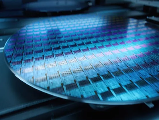
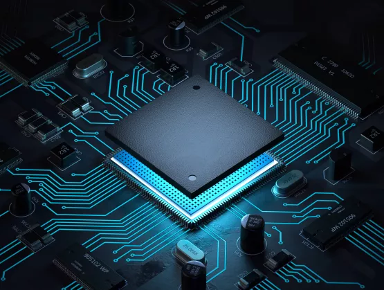
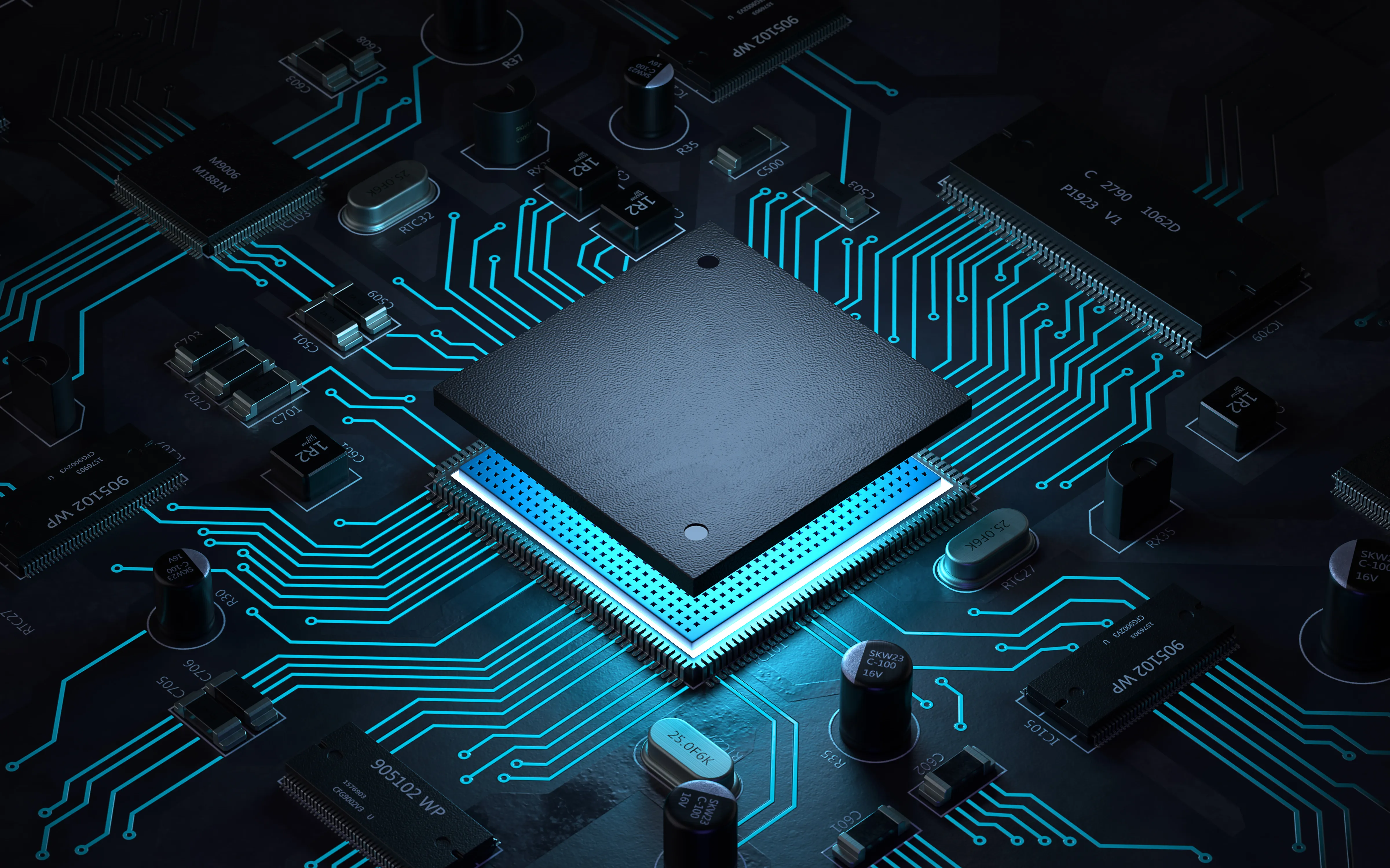
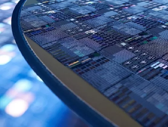
Fujimura: Manufactured masks and wafers are all curvilinear, even if the input CAD geometries are rectilinear (shown in Figure 1). It’s always been true that nature can’t make 90-degree turns, so sharp corners were always a matter of how closely you looked. These days, at the leading-edge nodes and their required resolutions, wafers and even masks are all visibly curvilinear as you can see in the graphic on the left in Figure 2.
Since the 1980s, both chip design and chip manufacturing systems have used axis-aligned rectangles, or “Manhattan” geometries, because 1) that was sufficient to design transistors and interconnect for the most part, and 2) CPU-based computer algorithms can be made much more efficient for Manhattan geometries. Curvilinear shapes can be piecewise linear polygons of some resolution, or spline-like formats that are curvilinear at any resolution, or specific curved patterns like circles and ovals.
Figure 1: All shapes on masks and wafers are curvilinear, even if the input geometries are Manhattan. Source: D2S
Smith: What are the benefits of curvilinear masks?
Fujimura: The manufacturing side of the semiconductor community knows that the best possible process window for wafer lithography is obtained by using curvilinear correction of mask shapes instead of Manhattan shapes. There have been numerous studies on the topic over several decades. The technique to generate purely curvilinear mask shapes is known as inverse lithography technology or ILT and is an advanced form of optical proximity correction (OPC).
At a February 2020 eBeam Initiative event, Micron Technology presented a study showing process window improvement up to 85% for advanced memory designs as a result of using curvilinear ILT (shown in Figure 2). Additionally, Ryan Pearman from D2S presented a study at Photomask Japan 2019 showing that it is preferable to move toward a completely curvilinear paradigm, not only because ILT is better, but because the mask manufactured will have reduced variability.
Figure 2: Micron Technology explained the benefits of curvilinear mask shapes for advanced memory at the eBeam Initiative event during 2020 SPIE Advanced Lithography Conference. Source: Micron Technology
Smith: If the benefits have been known for decades, why is it happening only now?
Fujimura: Several things happened at the same time. Multi-beam mask writing is now available. GPU acceleration for general computing has become mainstream. And wafer process window (resilience to manufacturing variation) is increasingly a problem for the leading-edge nodes as we are in the 5nm node, going to 3nm. Curvilinear ILT is needed much more now than before, will soon be needed for EUV lithography too, and is now possible because of multi-beam mask writing and GPU acceleration.
Smith: Curvilinear mask shapes enable curvilinear design shapes too?
Fujimura: Adoption of curvilinear mask shapes is the first step in targeting curvilinear shapes on wafers. Without curvilinear masks, it is difficult to target and reliably manufacture curvilinear designs. Curvilinear ILT works in the pixel-space to output the desired mask shape to maximize the process window for wafer lithography. A side effect of curvilinear ILT is that it can also take curvilinear targets as input. ILT, most likely GPU-accelerated ILT, works with rasterized input data, so the ILT algorithm itself is not affected even in runtime by having any amount of curvilinear design data.
The resulting mask shapes are written in multi-beam mask writers, which write pixels with doses. They too will write curvilinear masks at the same speed as Manhattan masks. Suddenly now, curvilinear designs can be handled by chip manufacturing equally well for the first time in about 30 years.
Smith: But curvilinear designs would be hard, right? There are a lot of tools that depend on the Manhattan assumption.
Fujimura: Yes, you’re right. We’re not going to suddenly see chips that have curvilinear routing all over the place, or curvilinear intra-connect in standard cells or memory cells. The entire physical design infrastructure that includes place and route, timing, custom layout, parasitic extraction and design rule checking moving to curvilinear design all at once is extremely unlikely. Could portions of these problems be tackled for specific cases over time as “hot spot” solutions? With GPU-accelerated SPICE being available now, as an example, if GPU acceleration is adopted for design, the same transformation that happened in manufacturing can (gradually) happen in design too. The key question is whether it’s worth the trouble.
Smith: Is it worth the trouble?
Fujimura: I don’t know if it’s worth the trouble for the entire infrastructure. For hot spots, “hot” for various reasons, there are certainly benefits. Jogging a 32-bit bus by one grid is certainly much more economical space-wise with curvilinear shapes. Inside standard cells or memory cells, there are certain types of features that pack better with curvilinear designs. In general, interconnect is the limiter to chip size of course, but there are always critical areas that could use help to shrink.
There are manufacturability benefits as well. In general, when something changes so drastically as this for the first time in 30 years, there’s bound to be some innovation that takes advantage of the discontinuity. Let’s see what the combined capitalistic power of the entire community might be able to come up with. The first thing is to let everyone know that curvilinear designs will be manufacturable today.
Hear insights from other leading electronic system design industry CEOs at the SEMI ESD Alliance CEO Outlook on May 18, 2021, 2:00pm-3:00pm PDT. Panelists will discuss the state of the industry along with their views of the outlook for the coming years. Registration is free for SEMI members.
About Bob Smith
Robert (Bob) Smith is executive director of the ESD Alliance, a SEMI Technology Community. He is responsible for the management and operations of the ESD Alliance, an international association of companies providing goods and services throughout the semiconductor design ecosystem.