downloadGroupGroupnoun_press release_995423_000000 copyGroupnoun_Feed_96767_000000Group 19noun_pictures_1817522_000000Member company iconResource item iconStore item iconGroup 19Group 19noun_Photo_2085192_000000 Copynoun_presentation_2096081_000000Group 19Group Copy 7noun_webinar_692730_000000Path
Skip to main content
Default Banner Image

GLOBALFOUNDRIES

Excellent news and exciting applications made headlines at the recent FD-SOI and RF-SOI events in Shanghai. During the FD-SOI day, Amazon/Blink and Intellifusion shared news about their new chips, and we got updates from GF and Samsung. The RF-SOI day featured a great talk with details about China Mobile's 5G plans, and peeks at Nokia's groundbreaking approach and Qorvo's outlook. [caption id="attachment_12354" align="alignright" width="300"] (Photo courtesy: Verisilicon)[/caption] The hall was absolutely full – with over 300 people attending each day. The FD-SOI event was by invitation only, and there were far more people wanting to attend than there was room for, even given the big room in which the events were held. The events got excellent coverage in the China tech press. For example, EEWorld started with an overview article and added five supporting pieces zooming in on key presentations and companies: one on GlobalFoundries, one on Samsung, one on Verisilicon, and two on Soitec (CEO and top exec interviews). These pieces are in Chinese, but just open the links through your favorite translation site. Many of the key slides are captured in these articles, so if you can't wait for the ppts to be posted on the SOI Consortium website, you can get some quick previews now. The Verisilicon PR folks also wrote up highlights of the FD-SOI event in real time with lots of great pictures – you can read that here. Many thanks to that team, too, for flagging the coverage in the China press and posting it on their WeChat account. On the RF-SOI side, the Simgui folks wrote that up – you can read it here. They also sponsored a gala dinner with awards given to Qorvo and SmarterMicro – you can read about that here. Most of the presentations will be posted on the SOI Consortium website over the next few weeks, at which point we'll cover them in-depth here at ASN. But for now, here's a quick round-up of some of the highlights. FD-SOI Highlights [caption id="attachment_12347" align="alignright" width="300"] (Courtesy: Blink, Verisilicon)[/caption] Boston-area based Blink, which makes very popular home security systems, was recently bought by Amazon (see their current product page here). They just taped out a new chip on Samsung's 28FDS FD-SOI technology, and they're really happy about it. “I believe for battery powered devices at home, FD-SOI is the way to go,” said Yantoa Jia, Head of ASIC China Ops at Blink. Their goal in the move from 55nm bulk to 28nm FD-SOI was to double battery life, add features and control costs: and they did it. Even adding two more CPU cores and lots more features, “The power drop is fantastic,” he said. Design was no problem, he continued, and there was plenty of IP. Once the new generation is officially announced, he promised to sit down with ASN and give us more details. Attendees also heard about a new chipset from Intellifusion, which is putting its face recognition technology onto GlobalFoundries' 22FDX FD-SOI with design house Verisilicon. CEO Nin Chen gave an impromptu talk about how their technology is used to find missing people and property. The new chip, which is especially designed for use in cities, is network-to-cloud leveraging AI. For his part Thomas Morgenstern, GlobalFoundries SVP and GM of the Dresden Fab 1, said they're seeing high yields and increasing capacity for 22FDX. The marketing and manufacturing ecosystem has been built around the fab in Europe. Now, he said, the key is to build an FD-SOI ecosystem in China. The market needs of China largely parallel those of Europe, he noted, for performance and efficiency at the right cost point. The ecosystem enables fast time-to-market and 1st-time-right. [caption id="attachment_12343" align="alignleft" width="300"] (Photo courtesy: Cadence)[/caption] Samsung SVP Gitae Jeong sees their FD-SOI technology as the right solution for the 4th Revolution, which includes everything from energy harvesting to self-driving cars. They've just taped out their first 5G mmWave cellular chip on 28FDS, he revealed. eMRAM is looking very good, only requiring three additional masks and getting stable yields from -40o to 105oC. 18FDS is on schedule, with PDK 0.5 now being released, and 1.0 on track for release in March 2019. They expect a very fast ramp, and are looking at a 35% area reduction, power cut in half and performance up 22% compared to 28FDS. RF-SOI Highlights [caption id="attachment_12350" align="alignright" width="300"] China Mobile, Project Manager Danni Song (Photo courtesy: Simgui)[/caption] When China Mobile talks, the world listens. Project Manager Danni Song presented again this year (she gave a great talk last year, too). China has a very ambitious 5G project underway, and under two years in which to roll it out. The biggest challenges are power consumption and cost (a problem made worse by the additional power amplifiers needed for MIMO). Can RF-SOI help solve these challenges, she asked? One thing she did clarify during the panel discussion was with respect to the mmWave part of the 5G puzzle. Their initial 2020 rollout will only focus on sub-6GHz, with mmWave following a year or two later. Michael Reiha, Head of RFIC R D at Nokia Mobile Networks clarified the worldwide 5G rollout during the panel discussion. Different locations on the planet have different histories and needs, so will rollout 5G in different ways. For historical reasons (and a lack of choice), the US will lead with mmWave, he said. Europe, meanwhile, will focus on 24GHz to meet the needs of automotive radar. In his presentation, Reiha described Nokia's approach to power amplifiers (PA), which is very different from what others are doing. With RF-SOI, he said, you can add sensors and logic for a level of preventative care, so you can gauge and protect your equipment using AI. He believes this disruptive approach will put them two years ahead of the industry, enabling massive MIMO to be deployed in dense urban areas with 60% lower power consumption and 50% savings in material costs. Go read about their Reefshark tech, he urged, which he says will beat GaAs. “The future is very bright with RF-SOI,” he concluded. “I can state that with confidence.” [caption id="attachment_12351" align="alignleft" width="300"] Julio Costa, Director of Technology Development, Qorvo (Photo courtesy: Simgui)[/caption] Julio Costa, Director of Technology Development at Qorvo sees it differently. Traditionally a GaAs house, all their RF-SOI work is fabless. While RF front end modules (FEMs) are loaded with RF-SOI, he said, and are a big winner for antenna tuning, Qorvo still sees GaAs for high-efficiency amplifiers and envelope tracking. But, he said, it will be a battle. GaAs wins in terms of area and power consumption he contends, but adds that SOI wins in terms of cost. Power levels, he predicts, will be the determining factor. So that's the quick overview – we'll drill down into the presentations as they're posted, so stay tuned!
Read More
The presentations from the SOI Consortium sponsored workshop held during Semicon West are now posted and freely available on the website – click here to see the full agenda with links to the presentations. The workshop, entitled 4G/5G Connectivity: Opportunities for the SOI Supply Chain, was well-attended and generated excellent discussions. If you don't have time to look at all of the ppts, here are quick overviews. Market Overview and FD SOI Opportunities, by Handel Jones, CEO, IBS. Handel Jones is an industry veteran, China expert and longtime follower of the SOI ecosystem. High performance with low power consumption are the key requirements for the continued growth in the semiconductor industry, he said, making FD-SOI the right choice for a wide range of products. Here's how he sees it: [caption id="attachment_12312" align="alignleft" width="300"] (Courtesy: IBS and SOI Consortium)[/caption] He estimates the yearly TAM (total available market) for FD-SOI based products in the range of $46 billion over the next 10 years, largely driven by needs for ultra-low power and RF integration. He goes on to break out volumes by applications (including ISPs – image signal processors; and CIS – CMOS image sensors), foundry markets by feature dimension and to map out technology trends. Mobile Radio Transformation in the Age of 5G: A Perspective on Opportunities for SOI, Peter Rabbeni, Vice President, Globalfoundries. Peter Rabbeni is an RF expert par excellence, having overseen the shipping of over 35 billion RF-SOI products to date. In his presentation, he details how 5G NR (New Radio) sub-6GHz frequency band specifications significantly increase frequency range and channel bandwidth, and how new band support and MIMO complexity and die size per handset are driving complexity in RF FEMs. Furthermore, 5G/mmWave phased arrays are driving a paradigm shift in the approaches that can be taken, he explains, so greater integration is needed. Here's a great slide showing where GF's two main SOI technologies come into play: [caption id="attachment_12311" align="alignleft" width="1000"] (Courtesy: GlobalFoundries and SOI Consortium)[/caption] Empowerment of 5G with SOI-Based Technologies, Emmanuel Sabonnadière, CEO, Leti-CEA. [caption id="attachment_12310" align="alignleft" width="300"] (Courtesy: Leti and SOI Consortium)[/caption] Working in partnership with industry leaders around the world, Leti has been the research powerhouse behind all things SOI since the early 1980s. In fact Reuters ranks them #2 in their most recent list of the World’s Most Innovative Research Institutions. This presentation reviews the key technical benefits of FD-SOI for IoT and IMT (that's international mobile communications, btw). Engineered Substrates – at the Foundation of 5G, Thomas Piliszczuk, Executive Vice President, Soitec. This presentation really puts the context around engineered substrates. Here are two excellent and useful slides here that identify which engineered substrates go where in the 5G world, and the engineered substrates that Soitec provides. Check these out: [caption id="attachment_12309" align="alignleft" width="1000"] (Courtesy: Soitec and SOI Consortium)[/caption] [caption id="attachment_12308" align="alignleft" width="1000"] (Courtesy: Soitec and SOI Consortium)[/caption] Ultra-thin Double Layer Metrology with High Lateral Resolution, Bernd Srocka, Vice President, Unity GmbH. [caption id="attachment_12307" align="alignleft" width="300"] (Courtesy: Unity and SOI Consortium)[/caption] In case you're not familiar with them, Unity provides a wide range of solutions in metrology and inspection. Both the top silicon layer and BOX layer of wafers for FD-SOI applications have draconian requirements that have required new approaches in metrology to ensure the thickness and homegeneity control of these very thin layers. China 5G Plan and SOI Ecosystem, Jeffrey Wang, CEO, Simgui. Shanghai-based Simgui partners with Soitec, using SmartCut™ technology for the production of RF-SOI wafers. It is doubling its capacity to reach 400K over the next year, and expanding into 300mm. China is aggressively working on 5G and plans to deploy 5G commercialization in 2020. Jeff Wang's is a terrific presentation detailing the rollout. (BTW, in addition to the massive funding effort underway, the government created the National Silicon Industry Group (NSIG) to support the semiconductor material ecosystem in China. You'll want to keep up with what's going on here). Here's the slide that summarizes the SOI ecosystem in China – the presentation then goes on to detail who does what. [caption id="attachment_12306" align="alignleft" width="1000"] (Courtesy: Simgui and SOI Consortium)[/caption] Inspection and Metrology Relevance in SOI Manufacturing, Jijen Vazhaeparambil, Vice President General Manager, KLA-Tencor. [caption id="attachment_12305" align="alignleft" width="300"] (Courtesy: KLA-Tencor and SOI Consortium)[/caption] K-T has played a strategic role in the SOI story going back for decades (and in fact they wrote a piece for the third edition of ASN back in 2005!), ensuring metrology innovations for things that hadn't previously need detection and measurement. With each new set of requirements, they rose to the occasion with wafer metrology solutions that helped increase quality and decrease costs. This presentation recaps some of them.
Read More
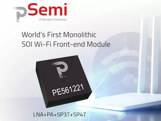
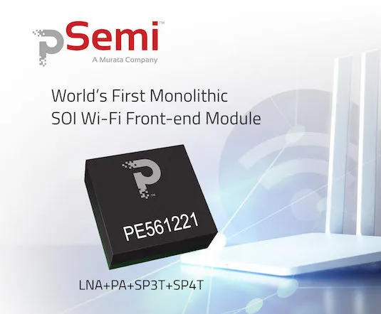
pSemi (formerly Peregrine, now a Murata company) has staked its claim for having the world's first monolithic SOI Wi-Fi front-end module (FEM)—the PE561221. This 2.4 GHz Wi-Fi FEM is the first to integrate a low-noise amplifier (LNA), a power amplifier (PA) and two RF switches (SP4T, SP3T) on a single SOI CMOS die. pSemi says it's ideal for Wi-Fi home gateways, routers and set-top boxes (read the full press release here). Driving this is the new WiFi standard, IEEE 802.11ax, which launches next year. While it's largely meant to tackle issues with WiFi in crowded places, it's also going to be welcome in high-demand home situations. (There's a good piece on the NetworkWorld site on what 802.11ax will do compared to the current 802.11ac – you can read it here). [caption id="attachment_12252" align="alignright" width="300"] The PE561221 uses a smart bias circuit to deliver a high linearity signal and excellent long-packet EVM performance. (Courtesy: pSemi)[/caption] With new standards come new challenges. pSemi explains their PE561221 uses a smart bias circuit to deliver a high linearity signal and excellent long-packet error vector magnitude (EVM) performance. “Traditional process technologies struggle to keep up with both performance and integration requirements, and only SOI can offer the ideal combination of integration and high performance,” says Colin Hunt, vice president of worldwide sales at pSemi. The monolithic die uses a compact 16-pin, 2 x 2 mm LGA package ideal for either stand-alone use or in 4 x 4 MIMO and 8 x 8 MIMO modules. It is based on pSemi’s UltraCMOS® technology platform—a patented, advanced form of SOI that offers superior performance compared to other mixed-signal processes. UltraCMOS technology also enables intelligent integration, notes pSemi—the unique design ability to integrate RF, digital and analog components on a single die. Volume-production parts and samples of the PE561221 are now available from pSemi. And this is just the beginning: while the PE561221 is the first product in the pSemi Wi-Fi FEM portfolio, the product roadmap includes 5 GHz Wi-Fi FEM solutions. The folks at pSemi have been doing RF-SOI for 30 years now, and recently shipped their 4 billionth chip. For the last five years, they've partnered with GlobalFoundries.
Read More
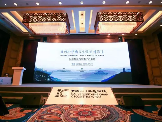
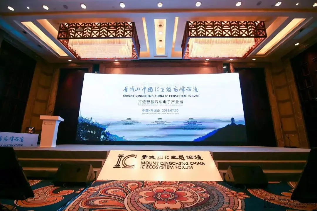
FD-SOI was a very important topic during the recent Mount Qingcheng China IC Ecosystem Forum. To situate things, Mount Qingcheng, with its lush hills and waterways, is located just outside of Chengdu. That of course is where GlobalFoundries is building its new fab, which will be the first in China to run FD-SOI. Chengdu is also a key city in China's automotive electronics landscape. [caption id="attachment_12236" align="alignright" width="300"] (Image Courtesy: VeriSilicon)[/caption] The theme of the forum was Building a Smart Automotive Electronics Industry Chain. Over 260 decision-makers from government, academia and industry attended – and the SOI Consortium had a significant presence. The event was chaired by Wayne Dai, CEO/Founder of consortium member VeriSilicon, and tireless champion of the the FD-SOI ecosystem in China and worldwide. Morning keynotes were given by: Carlos Mazure, Soitec CTO and SOI Consortium Executive Co-Director; Mark Granger, GF's VP of Automotive Product Line Management; and Tony King-Smith, Executive Advisor at AImotive, a GF 22FDX customer. BTW, transcripts of all the talks are available through Gasgoo, China's largest automotive B2B marketplace. You can click here to access them. (They're in Chinese – but you can open them in the language of your choice using the major translation websites.) Chengdu Officials Affirm Support for FD-SOI Fan Yi, Deputy Mayor of Chengdu, spoke extensively of FD-SOI in his keynote on the importance of rapidly developing smart cars. He heralded the “spectacular” new GlobalFoundries fab there. Following a meeting with the company's top brass the day before, he affirmed GF's confidence in their investment. There is a solid roadmap for FD-SOI, he noted, and efforts are underway to accelerate the move into production and expand education and training. He cited the benefits of FD-SOI for the entire supply chain, from design through package and test, raising the level of the entire IC industry to new heights. The government, he said, attaches great importance to this enterprise. Their thinking regarding intelligent transport in China is integrated with the overall approach to smart cities. SOI Consortium Leads Industry Keynotes [caption id="attachment_12232" align="alignleft" width="300"] Wayne Dai, VeriSilicon Founder and CEO (Photo courtesy VeriSilicon)[/caption] In his opening remarks, Wayne Dai emphasized the need for China to seize the advantage in the next round of development opportunities in the automotive electronics industry. This year's Qingcheng forum, he noted, brought together key representatives from across the supply chain, from of the highest to the deepest reaches of the smart car electronics industry, and across markets, technologies, solutions, industrial ecosystem, standards and regulations. In his talk on how FD-SOI is boosting the accelerated development of automotive electronics, Carlos Mazure presented the SOI Industry Consortium. He noted that the Consortium promotes mutual understanding and development across the ecosystem. SOI is already present throughout automotive applications, he noted. There are currently about 100mm2 of SOI per car, in such diverse areas power systems, transmissions, entertainment, in-vehicle networking and more. SOI will experience especially high growth in electrification, information/entertainment, networking, 5G, AI/edge computing and ADAS. He then went on to give some history and an extensive overview of the major trends and highlights we've seen over recent years. He finished by giving examples of convergence across the supply chain with IC manufacturers working with automakers to lower power, increase processor performance and advance 5G. [caption id="attachment_12233" align="alignright" width="665"] Carlos Mazure, Soitec CTO and SOI Consortium Executive Co-Director; Tony King-Smith, Executive Advisor at AImotive and Mark Granger, GF's VP of Automotive Product Line Management (Photo courtesy VeriSilicon)[/caption] GF's Mark Granger addressed the rapid development of automotive electronics. In certain areas, he said, he sees growth rates of over 20%. They are working on building the Chengdu ecosystem, especially for design, and in cooperation with the rest of the supply chain. Furthermore, he reminded the audience, when you talk about cars, travel implies that you also talk about IoT as well as things like infotainment and integrated radar ICs. In addition to cost and power efficiencies, the AEC-Q100 standard for IC reliability in automotive applications is also pushing designers to turn to FD-SOI. In the GF meeting with Chengdu government officials (referenced above in deputy mayor Fan Yi's talk), he too confirmed their support of FD-SOI as a key technology for China. GF is currently cooperating with about 75 automotive partners, he said, and the company is looking to increase cooperation with partners in the Chengdu region. Tony King-Smith talked about the 22FDX test chip AImotive is doing with Verisilicon and GF. In case you missed it, in June 2017 AImotive announced its AI-optimized hardware IP was available to global chip manufacturers for license. AiWare is built from the ground up for running neural networks, and the company says it is up to 20 times more power efficient than other leading AI acceleration hardware solutions on the market. In the same announcement, they revealed that VeriSilicon would be the first to integrate aiWare into a chip design,and that aiWare-based test chips would be fabricated on GF's 22FDX. The chip is expected to debut this year. While the afternoon agenda was not specific to FD-SOI, it did focus on the "smart cockpit" and "intelligent driving", with talks by nine leading players in China's automotive IC and investment communities. ~ ~ ~Note: Many thanks to the folks at VeriSilicon, who wrote up this event for their WeChat feed, and shared photos with us here at ASN.
Read More
GlobalFoundries has announced that the company’s 22nm FD-SOI (22FDX®) technology has delivered more than two billion dollars of client design win revenue. With more than 50 client designs, 22FDX is being used in power-optimized chips across a broad range of high-growth applications such as automotive, 5G connectivity and IoT. Their clients chose it for the significant reductions in power and die size relative to a traditional bulk CMOS process, says the company. 22FDX offers the industry’s lowest operating voltage, delivering up to 500MHz frequencies at only 0.4 volts. The technology also delivers efficient single-chip integration of RF, transceiver, baseband, processor, and power management components, “...providing an unparalleled combination of high performance RF and mmWave functionality with low-power, high density logic for devices that require long-lasting battery life, increased processing capability, and connectivity.” 22FDX is in early production, with yields and performance matching client expectations. A recent VLSI Research survey indicated that FD-SOI technology is seen as a complementary technology to FinFET. It's gaining traction in application spaces such as IoT, where power consumption is important and the product life is relatively short. “We’re only just beginning,” said GF CEO Tom Caulfied. “We have found a way to separate ourselves from the pack by emphasizing our differentiated FD-SOI roadmap and client-focused offerings that are poised to enable connected intelligence. We will continue to build on our momentum and look for ways to expand our reach to address the evolving needs of the industry.” Here's a sampling of customer quotes from the press release (read more here): “At Synaptics, as we expand upon our industry-leading mobile and PC businesses to include delivering new and innovative products that address the booming IoT market, we require the best available technologies to enable us to deliver top-notch solutions including voice and multimedia processing capabilities for our customers,” said the company's CEO, Rick Bergman. “GF’s 22FDX technology delivers a potent mix of low static and dynamic power along with excellent performance to give us a great platform for our world-class products.” “As our customers increasingly demand more from their mobile experiences, our partnership with GF on its 22FDX technology is critical to differentiate ourselves in the competitive market and deliver powerful and efficient mobile SoCs,” said Rockchip CEO Min Li. “Our goal has always been to provide more secure, connected experiences for drivers. Combining our leadership in radar technology with GF's 22FDX automotive-qualified process, we are able to deliver a cost-effective, high performance, low power solution that opens new opportunities for car manufacturers to provide better experiences for drivers around the world," said Kobi Marenko, CEO of Arbe Robotics. “The automotive industry realizes that assisted driving solutions require more camera information besides Radar and Lidar, integrating information from multiple cameras. The resulting DreamChip multi-core vision processor platform, based on the 22FDX process is providing European auto makers and Tier 1 automotive component suppliers with a platform from which they can create custom derivatives with a massively reduced time to market," said Dream Chip Technologies CEO Jens Benndorf. “With 22FDX, the value proposition for us is the potential power and area savings, two key metrics for our highly optimized LTE NB-IoT and CAT-M chipsets. In addition, leveraging the growing ecosystems of IP available in the 22FDX process helps to accelerate time to market,” said Peter Wong, CEO at Riot Micro, which designs purpose-built silicon for wireless IoT applications. (Read more about that here.) GF adds that it is preparing to deliver 12FDX™ technology, which will provide a full node scaling benefit and improved power efficiency for a new generation of applications, from edge-node artificial intelligence and AR/VR to 5G networking and ADAS.
Read More
That FD-SOI can be a key to achieving near-threshold voltage design was an important point made during a #55 DAC expert panel. Entitled How Close to Threshold-Voltage Design Can We Go Without Getting our Fingers Burnt? the session was organized by Jan Willis of Calibre Consulting. Turnout was excellent. Btw, Jan (herself an EDA expert) was one of the original advisors in the formation of the SOI Consortium, and while this DAC panel was not meant to be about FD-SOI, it turned out be a focal point. Near-threshold voltage design* is an especially hot topic for IoT and edge-computing designers, for whom balancing performance, reliability and extremely low power is generally challenge #1. For them, the ability to get chips working at very low voltages translates into battery life savings. The original goal of the panel was “...to explore how far below nominal voltage we can design, in what applications it makes sense and in what ways it will cost us.” The description in the #55 DAC program noted that “Energy consumption is the driving design parameter for many systems that must meet 'always-on' market requirements and in IoT in general. For decades, the semiconductor industry has attempted to leverage the essential principle that lowering voltage is the quickest, biggest way to reduce energy for a SoC. Some today contend sub-threshold voltage design is viable while others argue for near-threshold voltage design as the minimum.” (Update 2 August 2018: a complete video of this panel is now available on YouTube -- click here to view it.) [caption id="attachment_12035" align="alignnone" width="958"] #55 DAC Expert Panel: How Close to Threshold-Voltage Design Can We Go Without Getting our Fingers Burnt? Left to right: Brian Fuller, Arm (moderator); Scott Hanson, Ambiq Micro; Lauri Koskinen, Minima Processor; Mahbub Rashed, GlobalFoundries; Paul Wells, sureCore. (Organized by Jan Willis of Calibre Consulting)[/caption] The panelists included: Scott Hanson - Ambiq Micro Mahbub Rashed - GLOBALFOUNDRIES Lauri Koskinen - Minima Processor Paul Wells - sureCore Ltd., Sheffield Brian Fuller of Arm served as moderator. [caption id="attachment_12033" align="alignright" width="200"] Panel organizer Jan Willis, Calibre Consulting[/caption] Following the panel Jan published the following excellent recap on LinkedIn. She graciously agreed for it to be reprinted here in ASN, for which we thank her. So without further ado, read on! #55DAC Expert Panel on Near-Threshold Voltage Sees Growing Opportunity Despite ChallengesFirst published on LinkedIn, June 27, 2018 by Jan Willis, Strategic Partnerships Marketing Executive Brian Fuller, Arm, skillfully guided a group of experts through the challenges of near-threshold design to conclude that the adoption is going to start gathering pace in a panel session at the 55th DAC in San Francisco on Monday, June 25. Scott Hanson, CTO of Ambiq Micro, led off by saying the list of what's not challenging is a much shorter list but that by taking an adaptive approach, they have been successful. It's required innovating throughout the design process including test where Scott said they had create their own "secret sauce" to make it work. Later on in the panel, Scott described designers in near-threshold as "picojoule fanatics" to overcome the limitations in design tools which are geared towards achieving performance goals. Lauri Koskinen, CTO of Minima Processor, agreed that adaptivity is key. Minima says it has to be done in situ in the design to make it robust for manufacturing while useful across more than one design. Later in the panel, Lauri indicated that FD-SOI is like having another knob available for optimizing energy in the Minima approach to near-threshold design. Mahbub Rashed, head of Design and Technology Co-Optimization at GlobalFoundries, highlighted the need for more collaboration between EDA, IP, and foundries to support near-threshold design but noted a lot of progress has been made on FD-SOI processes. Mahbub cited models down to 0.4V for FD-SOI processes are available now and GlobalFoundries is able to guarantee yield. Paul Wells, CEO of sureCore, validated that sureCore has bench marked their memories on GlobalFoundries FD-SOI with success. He reflected that FD-SOI has rapidly established itself as cost effective for a number of emerging markets. The panel all agreed that achieving quality on the memory at near-threshold voltage was much tougher than for digital IP. [Editor's note: sureCore's CTO wrote an excellent summary of their SRAM IP for FD-SOI in ASN back in 2016 – you can still read it here.] Paul went on to summarize at the end of the panel that near-threshold voltage is the way of the future and that it's gathering pace. Mahbub called upon the EDA community to step up to improve the tools for low energy design. Lauri and Scott both summarized that there were drivers emerging that will grow the addressable market for near-threshold voltage design. Lauri pointed to growth coming from the applications that require edge computing which he thinks will require near-threshold voltage design. Scott concluded the panel by pointing out that there's been a tremendous increase in performance of near-threshold voltage designs which will increase the addressable available market in the future. ~ ~ ~ This piece was first published by Jan Willis on LinkedIn, June 27, 2018. Here is the original. * As explained by Rich Collins of Synopsys in the TechDesign Forum: "Operating at near-threshold or sub-threshold voltages reduces static and dynamic power consumption, at the cost of design complexity. [...] A transistor’s threshold voltage (Vth) is the voltage at which the transistor turns on. Most transistor circuits use a supply voltage substantially greater than the threshold voltage, so that the point at which the transistors turn on is not affected by supply variations or noise. [...] In sub-threshold operation, the supply voltage is well below the Vth of the transistors. In this region, the transistors are partially On, but are never fully turned. Near-threshold operation happens between the sub-threshold region and the transistor threshold voltage Vth, or around 400 – 700mV for today’s processes.
Read More
Dolphin Integration, a partner in the ENIAC THINGS2DO European FD-SOI project, showcased its achievements with PowerStudio™ during the project final review. Power Studio is Dolphin's cutting-edge EDA tool for safe Power Regulation Networks implementation. THINGS2DO, which stands for THIN but Great Silicon to Design Objects, was a 4-year, €120 million EU project (85% industry-funded) with over 40 partners that just finished up at the end of 2017. The goal was to build a design development ecosystem for FD-SOI. The project funded and supported the development of major FD SOI-based IPs and ASICs as well as EDA tools. (Another recent THINGS2DO announcement was Dream Chips’ ADAS SoC fabbed in GlobalFoundries’ 22FDX technology -- read about that here.) “Being involved in the THINGS2DO project was an opportunity for Dolphin Integration to start introducing FD-SOI in its automatic design methodologies,” said Frederic Poullet, Dolphin Integration’s CTO (read the press release here). “Dolphin Integration plans to offer a full suite of tools allowing its customers to implement right-on-first-pass Power Regulation Networks.” The company notes that THINGS2DO also proved that low power consumption makes FD-SOI a perfect fit for IoT and automotive applications. For instance, dynamic control of threshold voltage can be used to compensate for temperature variations, and to drive speed improvements by 200% in ultra-low voltage applications. Dolphin Integration provides energy efficient IPs and ASIC services dedicated to the low-power application market and supports its internal teams with tailor-made software tools. To address the specific needs of its customers in low-power design, Dolphin developed PowerStudio™, a global solution for the optimization of Power Regulation Networks (PRNet) to be used at an early stage of the SoC design process. In particular, it addresses new design challenges in noise and power supply integrity. The first module of PowerStudio™ will also embed architecture optimization features at the schematic level, in terms of FoM-based cost optimization, mode management, margin cuts and integrability rate-based risk optimization. Btw, Dolphin Integration Director Frederic Renoux gave an excellent great presentation at an SOI Consortium event in Nanjing, China last year, entitled Embedding power regulation activity control networks for best SoC PPA. Dolphin Integration joined Global foundries’ FDXcelerator™ Program last year (read the press release here) to streamline design in 22FDX®. "Our comprehensive and robust library of voltage regulators, power gating cells and logic modules, enables to deal cost-effectively and securely with power distribution, power gating, power monitoring and power control of any SoC design in 22FDX," Michel Depeyrot, Dolphin Integration's Chairman, said at the time. "As connected devices sleep most of their time, users of 22FDX also benefit from our ultra-low power and accurate oscillators to design an always-on RTC which consumes as little as 60 nA." See the Dolphin Integration website for the full catalog of their IP, EDA and ASIC/SoC service offerings, including for GF's 22FDX.
Read More
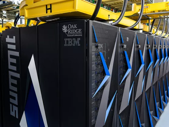
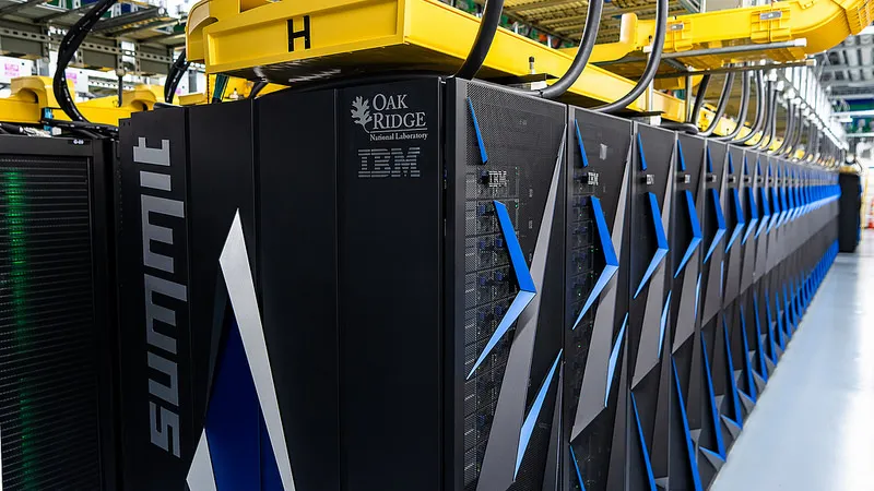
The CPUs in Summit, the world's new fastest supercomputer are built on 14nm FinFET-on-SOI technology. Yes, those IBM Power9 CPUs are fabbed by GlobalFoundries (you'll also find them in the z14, the most recent in IBM's z-series of servers – a series that's been on various iterations of SOI since its launch in 2003, btw). Summit's at the U.S. Department of Energy’s Oak Ridge National Laboratory (ORNL) in Tennessee, USA. It is now the top US supercomputer, and it's for science. The IBM-built Summit currently claims the spot in the Top500 as the world's smartest and most powerful supercomputer. “It is capable of performing 200 quadrillion calculations per second — or 200 petaflops — making it the fastest in the world,” says IBM's Dr. John E. Kelly, III, SVP, Cognitive Solutions and IBM Research. “But this system has never been just about speed. Summit is also optimized for AI in a data-intense world. We designed a whole new heterogeneous architecture that integrates the robust data analysis of powerful IBM Power CPUs with the deep learning capabilities of GPUs. The result is unparalleled performance on critical new applications.” And if that's not impressive enough for you, it's also #5 on the Green500 list for the world's most energy-efficient computers, posting Power Efficiency (GFlops/watts) of 13.889. [caption id="attachment_11940" align="alignright" width="300"] Summit supercomputer nodes: The IBM-built Summit supercomputer is the world's smartest and most powerful AI machine. It consists of 4,600 individual nodes. Each node contains two 22-core 3.07GHz IBM POWER9 CPUs, which are built on GlobalFoundries' 14nm HP FinFET-on-SOI technology, as well as six NVIDIA Telsa GPUs. (Photo Credit: ORNL).[/caption] As GF noted when they announced the technology in the fall of 2017 (read the GF press release here), their 14HP is the industry’s only technology to integrate a FinFET transistor architecture on SOI. Featuring a 17-layer metal stack and more than eight billion transistors per chip, the technology leverages embedded DRAM and other innovative features to deliver higher performance, reduced energy, and better area scaling over previous generations to address a wide range of deep computing workloads. These technologies have long, deep histories (and were developed in close collaboration with SOI wafer leader Soitec). Here at ASN we have a fabulous archive of pieces contributed by IBM explaining the genesis of the technology – they're great reads and still entirely pertinent: FinFET on SOI: Potential Becomes Reality (by T.B. (Terry) Hook et al, 2013) – this presents the key technical data. IBM: Why Fin-on-Oxide (FOx/SOI) Is Well-Positioned to Deliver Optimal FinFET Value (by Terry Hook, 2012) – this great piece busts myths and clearly explains why FinFETs on SOI deliver top performance. IBM: FinFET Isolation Considerations and Ramifications – Bulk vs. SOI (by Terry Hook, 2013) – explains why and how SOI increases operating voltage range, simplifies processing, reduces variation, lowers soft error rate, and enables higher circuit density. Embedded Memories in SOI – (by Subramanian S. Iyer, 2006) explains the importance of SOI in the memory part of the chip design equation. [caption id="attachment_11939" align="alignleft" width="300"] The IBM POWER9 processor delivers unprecedented speeds for deep learning and AI workloads. IBM Engineer, Stefanie Chiras tests the IBM Power System server in Austin, Texas. (Photo Credit: Jack Plunkett/Feature Photo Service for IBM).[/caption] As ORNL noted in its press release (you can read it here), the first projects will apply machine learning and AI to astrophysics, materials science, cancer research and systems biology. BTW, Summit also has a slightly smaller sister machine called Sierra, going in at the Lawrence Livermore National Laboratory (part of the Department of Energy's National Nuclear Security Administration). With 4,320 nodes (each also containing two 22-core 3.07GHz IBM POWER9 CPUs, which are built on GlobalFoundries' 14nm HP FinFET-on-SOI technology, but just four NVIDIA Telsa GPUs), Sierra's claimed the #3 spot on the June 2018 Top500 list of the world's most powerful supercomputers. And the Power 9 is now finding it's way into major data centers – like Google's (read about that here). There have been some good pieces in the press about it, including in Forbes and The Motley Fool. So yes, clearly there are exciting markets for FinFETs on SOI!
Read More
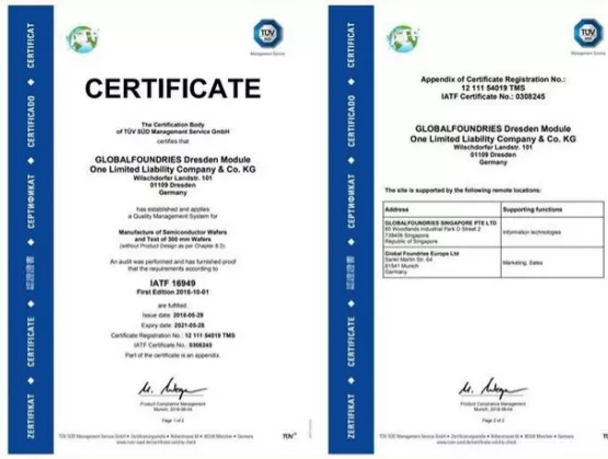
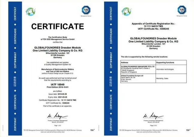
[caption id="attachment_11914" align="alignright" width="150"] Mark Granger, GlobalFoundries' VP Automotive Product Line Management[/caption] GF's 22FDX® (22nm FD-SOI) offering is on an automotive roll. The technology platform has been certified for several key automotive standards, and GF has announced an exciting new ADAS customer in Arbe Robotics. In addition to sharing info from various press releases and blogs, ASN also had a chance to catch up with Mark Granger, GF's VP for automotive, who provided some great insights. Read on! Taking the Heat When it comes to compliance, automotive industry standards are excruciatingly rigorous. Every part that goes into a car must adhere to the relevant standards: chips are no exception. One such standard is the AEC – Q100, a “Failure Mechanism Based Stress Test Qualification For Integrated Circuits”. The AEC – aka the Automotive Electronics Council – handles those testing standards and certification. Grade 2 means a technology is certified for the -40°C to +105°C ambient operating temperature range. To achieve Grade 2 certification, devices have to successfully withstand reliability stress tests for an extended period of time over the specified temperature range. GF recently announced that 22FDX has been AEC Q100 Grade 2 certified (press release here). However Granger adds that for their customers, they've added additional headroom that takes them to 125°C. They're now working on Grade 1 certification, he says, which means the devices are certified to handle junction temperatures up to 125°C (and there again, GF has added additional headroom that takes them to 150°C). That should be done by the end of 2018. The ability you get with FD-SOI to tune the transistors using body biasing is really beneficial here, he says. For GF, the 22FDX qualifications exemplifies their commitment to providing high-performance, high-quality technology solutions for the automotive industry. The automotive industry is driven by a “zero excursions – zero defects” mindset, says Granger, and that drives the foundry, too. SOI has been used for decades across industries where heat and electromagnetic radiation are challenges, bringing soft error rates (SER) down by orders of magnitude, notes Granger. (SOI, btw, essentially eliminates what are known as Single Event Upsets (SEU) caused by latch-up, which in turn brings down SER.) That in turn, ties into the FIT (failure in time) rate – and that's part of the ISO 26262 “Road vehicles – Functional safety” standard – where 22FDX is also certified. As a part of GF's AutoPro™ platform, 22FDX allows customers to easily migrate their automotive microcontrollers and ASSPs to a more advanced technology, while leveraging the significant area, performance and energy efficiency benefits over competing technologies. Moreover, the optimized platform offers high performance RF and mmWave capabilities for automotive radar applications and supports implementation of logic, Flash, non-volatile memory (NVM) in MCUs and high voltage devices to meet the unique requirements of in-vehicle ICs. GF's Fab 1 in Dresden, Germany (which is where they do 22FDX) also has achieved ISO-9001/IATF-16949 certification, which demonstrates that it is capable of meeting the stringent and evolving needs of the automotive industry. (IATF is the International Automotive Task Force. 16949 is a Quality Management System (QMS) certification specifically for the automotive sector.) Granger wrote a really informative blog on the GF website – you can read it here. It includes this graphic, indicating where in the car 22FDX-based parts are expected to go. [caption id="attachment_11913" align="alignleft" width="1000"] Here's how GF sees the applications for 22FDX and other chip technologies in automotive applications. (Courtesy: GlobalFoundries)[/caption] On Radar GF recently announced that Arbe Robotics selected 22FDX® as the process technology for its groundbreaking patented imaging radar. Arbe aims to achieve fully automated system capabilities and enable safer driving experiences for autonomous vehicles (read the press release here). As the first company to demonstrate ultra-high-resolution at a wide field of view, Arbe Robotics’ radar technology can detect pedestrians and obstacles at a range of 300 meters, in any weather and lighting conditions. The processor creates a full 3D shape of the objects and their velocity, and classifies targets using their radar signature. As Granger noted in his blog, “Radar is one of several sensor types used to detect objects near a vehicle, to enable features like adaptive cruise control. Lidar is another. It uses pulsed lasers to determine distance from an object by measuring the time it takes for the light to reflect back. However, lidar is currently expensive and is affected by weather conditions. Radar is less expensive, and higher-resolution radars promise to compete well with lidar in automotive applications, thereby enabling lower-priced vehicles to enjoy greater ADAS capabilities. 22FDX-based radar sensors can provide higher resolutions and less latency than current radar sensors at a very low total system cost.” While they may be complementary at first, there is a battle brewing between high-resolution radar and lidar, Granger told ASN. Putting their solution on 22FDX enables Arbe to achieve a 77 GHz mmWave radar and compete cost-effectively with lidar. “They wanted the best,” says Granger. 22FDX can achieve the requisite Ft and Fmax figures of merit. And with transistor stacking, they can also integrate the power amplifier (PA) on a single device. With the low inherent capacitance of the PA in 22FDX, you can get the high power output you need for mmWave but with low power consumption. GF blogger Dave Lammers has also written a great piece about the Arbe solution (you should read it: here's the link). “The company said its advanced technology allows the detection of small targets, such as a human or a bike even if they are somewhat masked by a large object such as a truck,” he writes. “The imaging radar can determine whether objects are moving, and in what direction, and alert the car in real-time about a risk. “While other car sensors can fail when it is raining, if there’s fog, and due to blinding lights such as a sudden reflection, Arbe’s radar is completely oblivious to all those factors. The custom designed radar processor creates a full real-time 4D image of the environment, and classifies targets using their radar signature.” Avi Bauer, Arbe's VP of R D, is now clearly an SOI fan. Lammers quotes him as saying, “With SOI the design is more straightforward, and (voltage) biasing allows you to do things that cannot be done in standard CMOS. For the transmit and receive modules, SOI’s higher resistivity substrate benefits the passive components – inductors and capacitors – and allows good isolation. High Q passives are important. At 22nm, SOI allows better performance overall.” Clearly good things are coming down the road for FD-SOI!
Read More