downloadGroupGroupnoun_press release_995423_000000 copyGroupnoun_Feed_96767_000000Group 19noun_pictures_1817522_000000Member company iconResource item iconStore item iconGroup 19Group 19noun_Photo_2085192_000000 Copynoun_presentation_2096081_000000Group 19Group Copy 7noun_webinar_692730_000000Path
Skip to main content
Default Banner Image

CMOS

Air pollution is a serious public health issue worldwide with airborne hazardous substances such as volatile organic compounds (VOCs), particle matter (PM), and nitrogen dioxide linked to a wide range of adverse health conditions. According to the World Health Organization (WHO), “the combined effects of ambient (outdoor) and household air pollution cause about seven million premature deaths every year, largely as a result of increased mortality from stroke, heart disease, chronic obstructive pulmonary disease, lung cancer and acute respiratory infections.” There’s also an economic impact of air pollution. Related illnesses and loss of life cost billions of dollars in healthcare services globally. And while we might think that air pollutants are only present outdoors, we’re more exposed to them – and they’re more potentially dangerous – indoors, where higher concentrations of volatile organic compounds (VOCs) produced by paint and furniture are a major concern. The COVID-19 pandemic has only heightened our awareness of the air we breathe. With recent medical research showing that viruses may be transmitted by attaching themselves to airborne particles, indoor air quality (IAQ) monitoring is becoming even more important. As we turn to VOC sensors for IAQ monitoring, it’s important to note that not all VOC sensors are equal. The current crop of low-cost VOC sensors are primarily total VOC sensors. Generally based on electrochemical or metal-oxide transducers, total VOC sensors provide a “grayscale” image of IAQ, which doesn’t differentiate among different gases. This limits people’s ability to make informed decisions regarding the level of threat to their health, since not all VOCs are equally hazardous and don’t require detection at the same concentrations. In addition, total VOC sensor technologies don’t support PM detection. This forces end-device designers to either add a module of optical sensors or switch to a completely different system. While optical sensors provide excellent performance, particularly for PM detection, they’re much more expensive, as well as more complex, bulky and power-hungry. This makes them ill-suited to resource-constrained portable devices where cost, size and power are at a premium. FBAR-based IAQ sensors emerge The shortcomings of available technologies for IAQ sensors has boosted the development of alternative solutions that provide better performance – in terms of both sensitivity and selectivity – as well as greater versatility, lower cost and smaller size. Acoustic sensor technologies featuring the latest advancements in film bulk acoustic resonator (FBAR) sensors are emerging as a leading candidate. Sensitivity is important in VOC detection because certain hazardous compounds, such as formaldehyde, are dangerous at very low concentrations. As highly sensitive devices, FBARs are a MEMS equivalent of a weight scale, but instead of detecting kilograms or grams, they can sense femtograms, which are just one-quadrillionth of a gram each. FBARS work by putting a thin film piezoelectric material into a mechanical resonance through application of an AC electric signal (GHz range) to a pair of electrodes on either side of the film. This resonant frequency is sensitive to the mass attached to the electrode surface. Whenever the mass attaches to the active area of the sensor, it produces a frequency shift, and this shift is proportional to the mass attached on the surface. Another major benefit of this approach is selectivity, which allows a device to distinguish between different target molecules or species. By placing a layer of material on the sensor –which is the functionalization layer – FBAR sensors display high selectivity on targeted materials. This allows the consumer to distinguish among different VOCs instead of just measuring a mixture of VOCs that vary in toxicity. Unlike older IAQ sensing technologies, FBAR sensors support functionalization layers comprised of different materials, from metal oxides and polymers to more exotic options such as carbon nanotubes and graphene. This increased versality makes it easier to use FBARs for a variety of applications, ranging from gas sensors to medical sensors. Sorex Sensors’ FBAR sensor in a 3mm x 3mm ceramic package FBAR technology is a perfect match for IAQ. In addition to high sensitivity and selectivity, it enables the manufacture of very small arrays, and it’s low-power, all of which make it a good choice for small portable devices. Plus FBAR technology is CMOS-compatible, so FBAR sensors can be made using standard MEMS processes and combined with integrated circuits fabricated using standard CMOS processes, making them cost-effective. With its origins at the University of Cambridge in the UK, Sorex Sensors is leading the commercialization of FBAR devices for sensing applications. After releasing our first product in 2019 – a standalone FBAR sensor and a development kit that can be used for particle monitoring – we’re preparing to release an FBAR sensor array that detects five different gases later this year. By offering specific functionalization layers for different targets, our new FBAR technology will provide a level of selectivity that other silicon-based sensors can’t achieve – particularly in light of FBAR’s low power consumption and very small size (less than 5mm x 5mm). In addition, the sensor’s targeted gases will include one of the main headaches in the IAQ space, formaldehyde, which is especially carcinogenic and is widely found in the varnishes used in furniture. We’re planning for this new iteration of our FBAR technology to help our customers sense in color rather than in grayscale – providing a level of granularity that’s unmatched in IAQ sensing. Check out the latest news about Sorex Sensors on our website and on LinkedIn. About the Author Mario de Miguel Ramos, Ph.D., is the co-founder and CEO of Sorex Sensors Ltd, a spin-out of the University of Cambridge, the University of Warwick, and the Universidad Politecnica de Madrid (UPM). Founded in 2017, the company focuses on the development of highly sensitive mass sensors based on film bulk acoustic resonators (FBARs). Dr de Miguel Ramos has been working in the field of FBARs for a decade. Prior to founding Sorex Sensors, he worked as a postdoctoral research associate at the Electronic Devices and Materials (EDM) Group at the University of Cambridge. He holds a master’s in Telecommunications Engineering and a Ph.D. in Electronic Engineering Systems, both from UPM. Sorex Sensors is a member of MEMS Sensors Industry Group®(MSIG), a SEMI technology community that connects the MEMS and sensors supply network in established and emerging markets to enable members to grow and prosper. Visit us today.
Read More
The combination of state-of-the-art semiconductor devices and upcoming manufacturing technologies for cost-effective processing of flexible film substrates has paved the way for a large variety of new applications in the emerging Flexible Hybrid Electronics (FHE).SEMI spoke with Professor Christoph Kutter, executive director, Fraunhofer EMFT, about current FHE technologies and market opportunities ahead of the Get Started with Flexible Hybrid Electronics workshop organized by Fraunhofer EMFT and supported by SEMI, 15 October, 2019, in Munich, Germany. To register for the event, click here.SEMI: Recent developments in thin semiconductors, new materials and cost-effective processing techniques have opened the door to a plurality of new applications and future products. What are the most innovative integration approaches?Kutter: Most interesting is the hybrid integration approach – the combination of most modern printing technologies and lithographically defined semi-additive copper wiring systems with state-of-the-art semiconductor components. Combining these best-of-breed technologies enables low-cost and high-volume printing but also ultra-low power electronics, which is important for every wireless device without or with limited power supply.SEMI: Integrating sensors, integrated circuits (IC), displays, antennas and communication devices on film substrates enables extremely thin and bendable form factors for applications where existing board-level technologies fall short. What are the key enabler technologies?Kutter: Key enabling technologies are fabrication of high-performance wiring patterns, integration of ultra-thin bare dies/components and ongoing advancements in roll-to-roll processing of film substrates. Besides the manufacturing technologies, materials such as electronic inks, substrates, isolation and passivation layers play a key role.SEMI: Are you currently working and experimenting on something particularly exciting?Kutter: We are in the process of developing an adaptive roll-to-roll direct imaging system that analyzes the position of the components manufactured before adaptive lithography steps are carried out in real time. We think that this concept will open up completely new processing possibilities for us. The technical infrastructure making this development possible is funded within the framework of the Research Fab Microelectronics Germany (FMD), the largest cross-site R D cooperation for microelectronics and nanoelectronics in Europe.SEMI: Can you share some details about the Fraunhofer EMFT roadmap?Kutter: Fraunhofer will push the hybrid integration – for example, combining printing technologies with high-performance CMOS – since we are convinced that hybrid integration is the only way to offer low-power systems for IoT with the highest performance and at the lowest cost. For this purpose, we are currently setting up a roll-to-roll die bond and component assembly machine.SEMI: What are your expectations for the future of flexible electronics and why would you recommend attending the workshop in Munich?Kutter: Flexible hybrid integration is becoming more important and offers the best of both worlds: mass volume printing technologies integrated with high performance ultra-low power electronics. You will see many examples of hybrid integration approaches during the workshop. This is a very important opportunity to highlight the latest developments in the semiconductor industry. Researchers, market analysts, material and product developers, and equipment suppliers will gather to provide insights into the latest flexible hybrid electronics innovations. We are particularly proud to organize this platform with SEMI and FlexTech Alliance.Agenda - Get Started with Flexible Hybrid ElectronicsLocation: Fraunhofer EMFT, Hansastrasse 27d, 80686 Munich, GermanyConference Chair: Prof. Dr. Christoph KutterENTRANCE Fees: 150 € VAT excl.Contact: [email protected] Prof. Dr. Christoph Kutter is the director of the Fraunhofer EMFT, focusing on sensing technologies based on silicon electronics and flexible hybrid integration technologies.Kutter completed his physics studies at TU Munich. In 1995, he earned his doctorate in physics at the University of Konstanz. Serena Brischetto is a marketing and communications manager at SEMI Europe.
Read More
According to market research and strategy consulting firm Yole Développement (Yole), the total market size of MEMS, sensors and actuators will double from $48 billion in 2018 to $93 billion in 2024.[i] The consumer market will continue to drive volume, with applications such as smartphones making up for in volume what they lack in average selling price (ASP). Stronger demand in automotive, biomedical/health, industrial, and voice-first applications (such as smart speakers) will support this upward trajectory. With so much growth ahead of us, how will the design and manufacture of MEMS keep pace with industry demand for higher levels of innovation and integration, lower cost and lower power, smaller footprints, and faster design cycles — all while meeting acceptable price points?We turned to a handful of MEMS manufacturing experts from SEMI-MSIG who will join us at SEMICON West 2019, July 9-11 at the Moscone Center in San Francisco, to explore the complexities of keeping pace with market demand for MEMS over the next decade.Address the Design GapMentor GM, ICDS Division Greg Lebsack and SoftMEMS President Mary Ann Maher see tremendous progress in the manufacturing supply chain for MEMS. At the same time, they acknowledge the significant gap that still exists in design capability for creating the billions of interconnected sensors required for future applications. Greg and Mary Ann will dive into the standards, ecosystem requirements and collaborative design solutions that will allow the micro-sensors industry to meet demand for next-generation wearables, Internet of Things (IoT) products and medical devices.Get Collaborative with Greg and Mary Ann: Addressing the Design Gap to Enable Next Generation Sensor-Based Products, SEMICON West, TechTALKS South, Thursday, July 11, 2019, 10:35-11:00 a.m. Register today.Get to a Really Big NumberFrom thousands of sensors and actuators in a single airplane to hundreds in a single car or a piece of factory equipment to the twenty-plus that ship in each of the hundreds of millions of the world’s smartphones, we aren’t even close to reaching the saturation point for these intelligent devices. SPTS Technologies EVP GM David Butler isn’t living on the Spaceship Enterprise (or the Millenium Falcon, come to think of it) when he says that we are going to get to a trillion sensors. It is going to happen. The questions are: how and when?Connect with David: Enabling the Age of a Trillion Sensors, SEMICON West, TechTALKS South, Thursday, July 11, 2019, 11:00-11:25 a.m. Register today.Shift to Automotive-GradeDemand for optical sensing technologies such as LIDAR is shifting sensor manufacturing requirements from consumer- to automotive-grade, with its enhanced lifetimes, temperature cycling and higher performance specifications. To meet demand, manufacturers are turning to wafer-level processing, since it complies with the hermetic sealing and dew-point control required for the more rigorous automotive-grade applications. EV Group Business Development Director Thomas Uhrmann, Ph.D., will provide an overview of the steps for manufacturing optical elements, including integration with CMOS circuitry, as he offers a window into the future of automotive packaging for sensors.Tune in with Thomas: Future Manufacturing Requirements for Automotive and Photonics Sensing, SEMICON West, TechTALKS South, Thursday, July 11, 2019, 11:25-11:50 a.m. Register today. Measure Twice, Cut OnceFaster time-to-market, improved device yield, and greater productivity in high-volume manufacturing are increasingly critical requirements for MEMS manufacturers. When a single manufacturing error can cost hundreds of thousands if not a million or more dollars — as well as months of development time — designers can save both time and cost by employing an integrated approach to MEMS design. Lam Research Sr. Director of Strategic Marketing David Haynes will explain how simulation, verification and process modeling can address MEMS-specific engineering challenges such as multi-physics interactions, process variations, MEMS + IC integration, and MEMS + package interaction. Using the right tools before committing to actual fabrication can make or break a project.Get Conceptual (and Practical) with David: Enabling Better MEMS from Concept to High-Volume Production, SEMICON West, TechTALKS South, Thursday, July 11, 2019, 11:50 a.m.-12:15 p.m. Register today.Navigate a Dynamic Foundry LandscapeWe’re still living in a one product-one process world when it comes to MEMS manufacturing. This makes bringing a new device to market both time-consuming and expensive. These challenges aside, the functional capabilities of MEMS, combined with small-footprint and low-power options, have made MEMS increasingly popular. How are market dynamics in MEMS manufacturing evolving to accommodate both demand for high-volume, lower-cost products such as MEMS microphones as well as high-value, lower-volume products such as biomedical devices, IoT products and industrial sensors? Rogue Valley Microdevices Founder CEO Jessica Gomez will explain how foundry consolidation through acquisition, collaboration with other ecosystem players, and specialization in vertical markets such as biomedical or optical are some of the approaches that are transforming the MEMS foundry landscape.Join the Evolution with Jessica: Consolidation, Collaboration, Specialization: How Will MEMS Fabs Manage Changing Dynamics, TechTALKS Stage South, Thursday, July 11, 2019, 12:15-12:40 p.m. Register today.i“Status of the MEMS Industry report,” Yole Développement (Yole), 2019 Edition.Maria Vetrano is a public relations consultant at SEMI.
Read More
Creating a custom Internet of Things (IoT) IC is challenging because it involves multiple design domains (digital, analog and RF). Creating a sensor-based IC that combines electronics that use the traditional CMOS IC design flow with a MEMS sensor on the same silicon die, however, can seem impossible. Couple the co-design and verification challenges with a lack of traditional process design kit (PDK) support for MEMS, and you have a tough road to travel to get your IoT designs to market.What can we do to make the sensor-based IoT design community successful?Understanding the ChallengesThe sensor-based IoT IC typically features a MEMS sensor (and optional actuator) that interact with the real world. Analog and digital circuitry processes the signals and sends them to a CPU. The CPU provides the “smarts” to process the data from the sensor and then sends processed data via a radio to the Internet; alternatively, the CPU could activate the actuator. A typical sensor-based IoT IC (Source: Mentor: A Siemens Business) Based on the complexity of the system, designers face many co-design challenges: Analog design requirements imposed by MEMS: MEMS devices often require high voltages and multiple power supplies; they emit small signals that need amplification and conditioning; and they are sensitive to the environment and require calibration. Design flow interactions: Parasitics from MEMS devices might affect circuits and vice versa. Circuit designers need MEMS models for impedance and timing. Integration: MEMS devices operate at different timescales than circuits, which adds a layer of complexity. Compounding the problem is a lack of MEMS PDKs and methods to tie together ICs and MEMS PDKs for integration and cross-verification. After conquering the co-design challenges, the design team has to address mixed-domain simulation challenges that include: Simulating the system: This requires verification of MEMS, digital, analog and RF circuitry with embedded software that runs on the CPU. Timescales: These vary widely, from a single deflection of the MEMS transducer in femtoseconds to a seconds-long simulation of the embedded software performing a measurement and transmitting data. Simulation time: Simulation of a behavioral digital design is extremely fast. However, the system simulation requires stand-in models that incorporate the behavior of the analog and MEMS block to simulate in an acceptable amount of time. The challenge of timescales for co-simulation. (Source: Mentor: A Siemens Business) MEMS is the KeyThe reality is that it’s the MEMS device that adds extra complexity to the sensor-based IC design and verification flow. To amplify the problem, the MEMS manufacturing process is not nearly as mature as the standardized IC process. For example, the standardized IC process includes ready-made PDKs that include everything designers need to move through design and verification flows. Foundries often provide soft and hard IP to quickly build-out design, and EDA tools provide high levels of automation enabled by abstraction and a standardized IC flow. How will MEMS-based design evolve?MEMS-based design must catch up to the standardized IC process. The first step is providing MEMS PDKs that include: Multi-physics domain design rules and material properties Packaging information Wafer and bonding information Fabrication information We must also tackle issues associated with these PDKs, including: Ownership, distribution and maintenance of the PDKs Consensus on the contents of the PDKs Merging of CMOS and MEMS PDKs The industry needs to move toward standardized MEMS manufacturing processes with available PDKs. Companies must provide IP and recommend structured design methods for co-design and verification of ICs that incorporate MEMS. How can EDA help with these flows?The EDA ContributionEDA companies must work with teams in the MEMS IC co-design space, collaborating with MEMS fabricators to help enable PDKs. By incorporating PDK support within their own tools, EDA companies can provide an integrated custom IC flow that allows teams to design and verify MEMS-based ICs. For details about this flow, click here to download the Mentor whitepaper: Fusing CMOS IC and MEMS Design for IoT Edge Devices.Greg Lebsack brings 25 years of executive and technical management experience — along with a proven track record of building strong teams and delivering predictable results — to his role as general manager of the ICDS division of Mentor, a Siemens Business. Lebsack joined Mentor in 2015 after that company acquired Tanner EDA, where he was president. Prior to Tanner EDA, he held management and technical positions in a number of different industries and companies, including Sprint, General Electric and McKinsey Co. Greg holds a bachelor’s degree in business administration from Northern Arizona University.Greg Lebsack recently presented on the topic of Integrated Co-design of MEMS/IC at the MEMS Sensors Technical congress, a technical conference organized by the MEMS Sensors Industry Group.
Read More
SEMI met with Erez Halahmi, vice president at 0eC SA, to discuss a new way to transfer information not only between chips but also between servers to reduce power consumption while boosting performance. The two spoke ahead of his presentation at the 3D Systems Summit, 28-30 January, 2019, in Dresden, Germany. To register for the event, please click here.SEMI: What is Zero energy connection’s (0eC) mission and vision and your role within the company?Halahmi: Prof. Naaman of the Weizmann institute of Science (Israel) and I founded OeC SA and invented the Zero energy connection (0eC) technology. OeC SA offers a completely new and innovative solution for interconnections, which dovetails with the current technological trend of “less is more.” In fact, we constantly search for a reduction in energy consumption in favor of capacity, all while simplifying manufacturing processes. We try to look at things differently. This is why our technology is so out of the box. It is a completely new way to transfer information, not only between chips but also between servers.SEMI: What projects are you currently working on that you think will make a difference in 2019?Halahmi: I am working on several diversified exciting projects including the development of a planar field emitter and a rechargeable battery with energy density higher than 1KWh/Kg. Planar field emission is a field emitter made with standard FAB processes that enable a pixelized matrix of emitters at the resolution of photolithography. The rechargeable battery is a novel battery type that delivers unprecedent energy density.SEMI: Your presentation at the 3D Systems Summit will focus on a new way to transfer data. Why is this a key topic?Halahmi: Metals have been used to transfer data since the realization of the first integrated circuit by Jack Kilby in 1958. What happened next? Photonics slowly entered the market supported by huge investments, and the global market grew over the years. However, even with such enormous growth, photonics is not easily integrated with CMOS processes and the market also faces the conversion energy issue on top of the rising costs of process change. Integrating photonics with CMOS requires converting an electrical signal to a photonic signal and back. This costs energy and adds circuitry complexity. What to do? We identified a need to create something out of the box – on one hand using the same CMOS processes without conversion, and on the other hand significantly increasing performance. More details will be released at my presentation at the 3D Systems Summit in Dresden. I am certain that you will find our invention very intriguing. SEMI: What do you think will be the main focus in the future?Halahmi: My belief regarding many aspects of our life is that history repeats itself. Look for example at the comparison Gallium Arsenide (GaAs) versus Silicon (Si). GaAs was never able to defeat the simplicity of Si. The same applies to data transfer. However, for a solution to overtake the metal interconnect, it is not enough to offer many advantages, but the same order of production simplicity should apply. Consequently, big companies will continue to focus on metal solutions for transferring data, though some smaller companies might adopt our technology due to its relative simplicity of production and great benefits.SEMI: What are your expectations for the summit in Dresden, and why do you recommend other industry leaders to attend the 2019 3D Systems Summit?Halahmi: The summit is a great opportunity to learn about new technologies and meet the people behind these innovations. It is a unique chance to meet and question the inventors themselves and learn more about your competitors. See you soon in Dresden!Serena Brischetto is a marketing and communications manager at SEMI Europe.
Read More
When developing industry forecasts, market analysts gather data from hundreds of companies to provide actionable insights on established technologies and to identify near-term business opportunities. As a developer of new MEMS and sensor technologies for a range of commercial applications, clients often ask us, “What’s going to be hot?” Gauging the promise of emerging technologies that are five to 10 years from commercialization requires taking a different tack.History tells us that most of today’s blockbuster MEMS products were born as academic research projects. Years of hard work by entrepreneurs, funded by millions of dollars, have turned proof-of-concept research into new commercial products. To identify up-and-coming technologies, we gather information straight from the source: academic conferences and articles.Chirp Microsystems is a good proof point of our research methodology: In my 2012 report on emerging technologies, I highlighted research from UC Berkeley and UC Davis on “In-Air Ultrasonic Rangefinding and Angle Estimation Using an Array of AlN Micromachined Transducers.” Soon after publication, the authors incorporated Chirp Microsystems to commercialize their technology for gesture- and fingerprint-recognition applications.After five years of development work, Chirp’s products are entering the marketplace. In February 2018, the global supplier TDK InvenSense acquired Chirp, underscoring the company’s commercial potential. At October’s SEMI-MSIG MEMS Sensors Executive Congress in Napa, Calif., Chirp’s CEO, Dr. Michelle Kiang, held attendees rapt as she described her company’s journey from startup to wholly owned subsidiary.There’s a methodThis year, I reviewed over 100 papers from top researchers presenting noteworthy technologies at the Hilton Head Workshop on Solid-State Sensors, Actuators and Microsystems. My criteria for selection were: commercial relevance; offers a solution to a known or anticipated problem; and technology game-changers. The following caught my eye: Event-driven sensors: Cleverly designed silicon MEMS that consume no power while standing by. A triggering mechanical or thermal event closes a contact within the sensor to activate its circuitry and telemetry. These sensors leverage existing fabrication methods, so they could become commercial products within five years for event monitoring and security applications. (UT Dallas, Northeastern University). Figure: 5-bit accelerometer having zero standby power. The device is open circuit until a threshold acceleration closes a mechanical contact. Source: University of Texas at Dallas. Thin film piezoelectric resonators: Advances in PZT deposition methods and process integration with CMOS were used to create monolithic acoustic waveguides for RF filtering in 5G applications. This new filter design, using existing scalable processes, is ripe for commercialization. (Purdue University, Texas Instruments) Intra-body communications: MEMS ultrasound transceivers, made from aluminum nitride, can send data directly through flesh at Mbit/s data rate. With trends toward networks of multiple implanted or wearable medical devices, this innovation would enable medically safe, secure, intra-body wireless communication. This early-stage work still needs in vivo validation and would likely require 10 or more years for development and regulatory approval. (Northeastern University) Screen- and 3D-printed sensors: One example of many exciting innovations using screen- and 3D-printing are potentiometric nitrate soil sensors. Low-cost and biodegradable, these sensors could be spread over huge areas to monitor a farm’s soil quality. Table-top and hobbyist tools are currently used to make screen- and 3D-printed devices, so new manufacturing equipment and infrastructure must be developed before commercial production could occur. (Purdue University) Biodegradable batteries: A paper-based battery that can deliver 0.5 uW of power, ingeniously using bacterial metabolism as the electrolyte. These batteries dissolve in water and could one day be used to power temporary medical implants or biodegradable sensors. This exciting proof-of-concept prototype will require significant process development and new manufacturing infrastructure for commercialization. (SUNY Binghamton) Figure: Paper-based battery dissolves in 60 minutes after immersion in water. Source: SUNY Binghamton To read more about these technologies, please download my presentation from SEMI-MSIG’s MEMS Sensors TechXpot at SEMICON West 2018.Alissa M. Fitzgerald, Ph.D., is the founder and managing member of A.M. Fitzgerald Associates, LLC, a MEMS and sensors development company in Burlingame, CA. She has over 20 years of engineering experience in MEMS design, fabrication and product development and now advises clients on the entire cycle of product development, from business and IP strategy to manufacturing operations. She is a frequent speaker at industry conferences and currently serves as a director of the Transducer Research Foundation, sponsor of the Hilton Head Workshop. She received her bachelor’s and master’s degrees from MIT and her doctorate from Stanford University in Aeronautics and Astronautics.For more information, visit: www.amfitzgerald.com
Read More
Materials innovation has always been vital to the semiconductor industry. In the past, it was high-κ gate dielectrics. Today, Cobalt is seen as a replacement for Tungsten in middle-of-line (MOL) contacts.What materials innovation will the future bring?A likely answer is Graphene, the wonder material discovered in 2004.Graphene is one atomic layer of carbon, the thinnest and strongest material that has ever existed. It is 200 times stronger than steel and the lightest material known to man (1 square meter weighing around 0.77 mg). It is an excellent electrical and thermal conductor at room temperature with an electron mobility of ~ 200,000cm2.V-1.s-1. At one atomic layer, graphene is flexible and transparent. Other notable properties of Graphene are its uniform absorption of light across the visible and near infrared spectrum and its applicability towards spintronics-based devices.Graphene and Moore’s LawMoore’s Law scaling can be broken down into 4 key areas: Lithography FET Advanced Packaging (2.5D and 3D IC) Interconnect Material Solutions for upcoming nodes are starting to emerge in the first two areas (EUV and Nanowire- or Nanosheet-based FET respectively). Graphene play an important role in the latter two areas. For advanced packaging, Graphene can be used as a heat spreader (to lower overall thermal resistance), or as an EM shield (to lower crosstalk) as part of a 3D IC package.Active Graphene device layers can potentially be stacked on top of each other using a low-temperature transfer process ( 400°C) to allow for a dense heterogeneous “memory near compute” configuration. This is an area DARPA is actively researching as part of its new $1.5 billion Electronics Resurgence Initiative.Regarding interconnects, Copper interconnects are running out of steam and becoming a major IC bottleneck (projected 40% total delay for 7 nm node). Graphene’s high electron mobility and thermal conductivity make it an attractive interconnect material for MOL and back-end-of-line (BEOL), especially at line widths 30 nm.Graphene Device ApplicationsGraphene-based semiconductor applications are already starting to hit the market. A fully integrated optical transceiver (with a Graphene modulator and photodetector) operating at 25 Gb/s/channel was on display at the recent Mobile World Congress in Barcelona. San Diego-based Nanomedical Diagnostics is selling a medical device that uses a Graphene biosensor. Europe-based Emberion is building Graphene optoelectronic sensors that might find a home in LIDAR applications, where there is currently a focus on improving sensing in low-light conditions.What will the overall Graphene roadmap in the semiconductor industry look like? The history of ion implantation serves as a good example of how a fundamental scientific discovery moves from the lab to the foundry floor.The dominant view in the semiconductor industry at the time was that ion implantation would not work in practice (vs. thermal diffusion) and that, if it did, it would only marginally improve the manufacturing yields of existing products. There was nothing obvious about the transfer of ion bombardment techniques from nuclear physics research to semiconductor production.Varian (led by British physicist Peter Rose) built a new, advanced ion implant tool that Mostek (DRAM manufacturer based in Texas) was able to use to create MOS ICs with clear competitive advantages. The successful collaboration between Varian and Mostek was the turning point in the development of ion implantation as a major semiconductor manufacturing process. Over the next few years, semiconductor firms used ion implantation in a growing number of process steps and, by the late 1970s, it became one of the main processes used in semiconductor manufacturing.Likewise, the Graphene world needs to work closely with the semiconductor industry to develop the tools and techniques required to solve fundamental issues around Graphene growth (good uniformity over large area, low defect density) and Graphene transfer (high throughput, CMOS compatible). It is only then will we fully realize a future that includes 2D materials.The first step in this process is cross-industry education and initiating the dialogue between semiconductor industry and graphene companies. The National Graphene Association will be hosting the largest gathering of graphene companies and commercial stakeholders at the Global Graphene Expo Conference, October 15-17, 2018, in Austin, Texas.Learn more about graphene at the upcoming Global Graphene Expo Conference with dedicated panels of experts and investors, and roundtable discussions on how Graphene will impact the semiconductor industry. The event promo code is SEMINGA. About the AuthorAnand Chamarthy is the CEO and Co-Founder of Lab 91, an Austin-based startup that is working towards Graphene/CMOS integration at the foundry level. Anand can be reached at [email protected]. About the National Graphene AssociationThe National Graphene Association is the main organization and body in the U.S. promoting and advocating for commercialization of graphene and addressing critical issues such as standards and policy development.
Read More
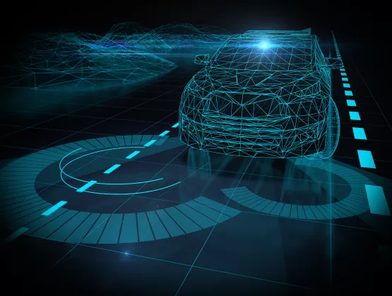
Driven by the adoption of evermore electronic components in end products, the semiconductor industry is facing a new era in which device scaling and cost reduction will no longer continue on the path followed for the past few decades. Advanced nodes no longer bring the desired cost benefit, and R D investments in new lithography solutions and devices below 10nm nodes are rising substantially. In order to satisfy market demands, the industry is looking for technology solutions to bridge the gap and improve cost/performance while at the same time adding more functionality through integration.More than-Moore devices (including MEMS and sensors, CMOS Image Sensors, power electronic, along with RF devices) represent this new functional diversification of technologies, combining performance, integration and cost not limited to CMOS scaling, and their importance will become more and more preponderant.In 2017, wafer demand for More than Moore devices1 reached almost 45 million 8-inch eq. wafers. This figure is expected to reach more than 66 million 8-inch eq wafers by 2023, showing an almost 10 percent growth during this period.This increase is supported by the famous megatrends detailed in the new analysis, Wafer Starts for More Than Moore Applications2, performed by Yole Développement (Yole). This analysis is relevant to the following markets: 5G with wireless infrastructure and mobile segments, mobile including additional functionalities, voice processing, smart automotive and electrification, AR/VR3, and AI4.For the first time, the market research and strategy consulting company presents a dedicated technology and market analysis focused on the overall wafer demand for More than Moore devices. The aim of this report is to give an overview of wafer shipments for More than Moore devices, from wafer size to semiconductor material substrate type including silicon, glass, SOI5, SiC6, SiGe7, GaN8, InP9, GaAs10, sapphire and ceramic, and thus identify business opportunities in the More than Moore industry.For over 20 years, Yole has been analyzing the industry evolution, discussing with leading companies to understand market challenges, and identifying technical breakthroughs. The Wafer Starts for More Than Moore Applications report is the result of this 20-year research. Yole’s analysts combine technical and market expertise to describe the More than Moore world. Market size (volume and value), substrate sizes and formats, value chain, technology processes and market drivers, business opportunities and competitive landscape are all part of Yole’s analysis.The various research teams at Yole, encompassing power electronics, imaging and sensing, RF and semiconductor manufacturing, collaborate to present an in-depth understanding of the current market evolution, taking into account innovations and emerging businesses. This methodology allows Yole to cover the overall megatrends and illustrate the links between wafer substrate, device, module, sub-system, system and high-end product.Under this dynamic ecosystem, the deployment of renewable energy sources and industrial motor drives as well as the electrification of the automotive industry are good examples of the impact of megatrends on the semiconductor industry development. They are directly impacting the power devices’ wafer market, resulting in an expected 13 percent CAGR between 2017 and 2023. Already in 2017, this market represented more than 60 percent of the overall wafer market for More than Moore devices, and is currently still dominating the More than Moore industry.5G is one megatrend driving wafer demand. 5G is leading the More than Moore evolution, bringing any service to any user, anywhere. Antennas and filtering functionalities are two of the key innovations of this evolution.Without doubt, the stringent requirements of 5G are driving increasing demand for RF components like RF filters, power amplifiers (PAs), and low-noise amplifiers (LNAs) to ensure access to tomorrow’s radio network.This year, Corning and Menlo Micro announced a major agreement to develop a DMS[11] product platform. Both partners propose an innovative approach based on TGV12 packaging technology. According to both partners, this technical choice allows them to cover operation of frequencies beyond 50GHz. Amongst the numerous megatrends, mobility is not far behind 5G. Demand for advanced mobile applications integrating more and more functionality is growing. In order to compete companies are developing smart combinations of devices such as fingerprint sensors, ambient light sensors, 3D sensing, microphones, and inertial MEMS devices. As an example, impressive developments focused on SOI-based NIR sensors have been released by SOITEC for front-side imager applications including advanced 3D image sensors. This technical evolution will clearly contribute, in the near future, to strong growth of the wafer market for MEMS and sensors. Additionally, the automotive industry, with the development of smart cars, has reached a new level of complexity requiring the development and integration of new sensors. In this context, many companies are aiming to extend their capabilities in ADAS13 and autonomous driving. Recently the leading company On Semiconductor acquired SensL Technologies, the leader in SPAD and LiDAR sensing products for automotive. This acquisition is one sign among many highlighting the evolution of this historic industry, searching for new expertise and welcoming new players, more aware of consumer habits and needs.Yole’s analysts expect smart automobiles to drive consistent growth of CIS14 and sensor wafer production over the next five years. It is fueled by the increasing integration of high-value sensing modules like RADAR, imaging, LiDAR and more. Although automotive will be mainly supported by these growth areas, historic MEMS and sensors such as MEMS pressure sensors and inertial MEMS will continue growing at a reasonable rate, supporting the standard automotive world.Yole Group of Companies including Yole, System Plus Consulting, KnowMade, PISEO and Blumorpho follows and analyzes the industry continuously. The Group has developed in-depth expertise and knowledge focused on the semiconductor manufacturing process and markets. Companies of the Group work together to understand the technical issues, identify business opportunities and propose valuable analyses.Yole invites you to an overview of the Wafer Starts for More Than Moore Applications report during the exclusive online event, titled “Wafer Starts for More than Moore Applications – Webcast”. This hourlong webcast takes place on June 28 at 5:00 PM CEST. The market research company will present key results of this report including megatrends, wafer market evolution and technical trends. Moderated by David Jourdan, Sales Coordination Customer Service at Yole, it welcomes the two leading companies, SPTS (an Orbotech Company) and Corning Precision Glass Solutions: "Trends in Wafer Processing Technologies for RF MEMS" – Speaker David Butler, Executive Vice President and General Manager at SPTS Technologies "Benefits of Through Glass Vias for RF applications" – Speaker: Ravij Parmar, New Product Development Manager for Corning Precision Glass Solutions These results will be also presented by the Semiconductor Software team at SEMICON West (Booth #1320), SEMICON Taiwan and SEMICON Europa (Booth #A-4667). Make sure to meet Yole’s analysts and get a valuable overview of the More than Moore industry. Agenda and more information are available on i-micronew.com. Stay tuned!About the authors:Amandine Pizzagalli is a Technology Market Analyst, Equipment Materials - Semiconductor Manufacturing - at Yole Développement (Yole). Amandine is part of the development of the Semiconductor Software division of Yole with the production of reports and custom consulting projects. She is in charge of comprehensive analyses focused on semiconductor equipment, materials and manufacturing processes. Emilie Jolivet is Director of the Semiconductor Software Division at Yole Développement, part of Yole Group of Companies, where her specific interests cover package assembly, semiconductor manufacturing, memory and software computing fields. 1 Including: MEMS sensors, CIS, and power, photonics and RF devices2 Yole Développement, March 20183 AR/VR : Augmented Reality/Virtual Reality4 AI : Artificial Intelligence.5 SOI : Silicon On Insulator6 SiC : Silicon Carbid7 SiGe: Silicon Germanium8 GaN: Gallium Nitride9 InP: Indium Phosphide10 GaAs : Gallium Arsenide111 DMS : Digital-Micro-Switch12 TGV : Through Glass Via13 ADAS : Autonomous Driving Assistance Service14 CIS : CMOS Image Sensor
Read More
The fast-growing automotive semiconductor market means big change for the IC supply chain. Beyond the obvious demands for reliability and traceability, the sector is moving towards simpler and lower-cost solutions while facing the daunting challenge of automating driving in a complex world. The need for simpler and cheaper automotive intelligence will likely drive acquisitions to build complete platform solutions that are easier to integrate. This demand has already spawned a market for pre-configured test cars to save developers time and money, and is driving LiDAR (Light Detection And RADAR) towards lower-cost, solid state solutions. “The growth of the automotive electronics market provides a great opportunity for the IC supply chain to differentiate on specialty processes and quality for the high-volume automotive business with its long design cycles,” says Scott Jones, principal, strategy, at KPMG, who will speak in the automotive program at SEMICON West. “This differentiation is a chance to reduce chip suppliers’ dependence on scaling volume for the mobile phone world with its short-cycle volatility of winning and losing sockets.” He notes that increasing demand for automotive ICs is also reinvigorating the eight-inch supply chain and spurring opportunity for specialty products such as compound semiconductor devices for power efficiency. Supplying the automotive market also means addressing automotive reliability requirements, which can be 10 times more stringent than for consumer devices. At the same time, the industry must sustain fast-paced development cycles required for the volume and diversity of low-cost IoT devices, manage the segmented supply chain for both those markets, and still spread development costs. Another big challenge for the supply chain will be to automate testing and update vast amounts of embedded software in these automotive devices. “The more complete solution a company can put together, the more the automakers will gravitate to it. They want simplicity,” Jones suggests. Smaller players will need to differentiate with IP and acquire other IP provider to build a broader platform, or be acquired and folded into an all-in-one solution.AutonomouStuff helps accelerate and simplify development of autonomous driving solutionsAutonomouStuff is helping to speed development of these platforms. The company has grown from a sensor distributor into a supplier in the emerging niche of vehicles preconfigured with key interfaces for sensors and controls. These interfaces can then be customized by integrating different components for developers to test their applications. AutonomouStuff offers developers a lineup of vehicle models pre-configured with the interfaces needed to add desired chips, sensors and software to develop their autonomous vehicle systems. Source: AutonomouStuff.“Whether they’re major chipmakers or AI software startups, they don’t have a year to build their own vehicle platforms themselves for developing autonomous vehicle systems,” says Wolfgang Juchmann, VP sales and business development at AutonomouStuff. Juchmann, a SEMICON West speaker, will bring a demonstration vehicle to the show. “In four to six weeks we can prepare a custom test car with selected sensors, enabling users to start testing their computer platforms and software. It’s faster and more cost-effective for us to supply the car with the needed interfaces.” He notes that developers are using some 300 AutonomouStuff vehicles in the field. AutonomouStuff customers are starting to transition from testing on a single car or two to testing on mini-fleets with 50 to 100 vehicles. Beyond sensors and pre-configured vehicles, the next step will be to add more data intelligence services to help with capabilities like tagging the data for training, Juchmann says. AutonomouStuff already offers hardware to support Baidu’s Apollo open-source software stack and data set. The company was recently acquired by the Swedish holding company Hexagon to help support expansion.CMOS silicon LiDAR nears automotive qualificationInnovations in the hyper-competitive LiDAR market, where burgeoning demand is driving the race to develop various types of solid-state devices, may also help reduce the cost of autonomous vehicles. Among the roughly 40 LiDAR suppliers, at least one – Quanergy – is taking advantage of 45nm and 32nm foundry CMOS volume production. The company uses voltage through the semiconductor stack to change the refractive index, controlling the phases of optical beams and the resulting interference patterns of light exiting the chip to quickly steer the laser beam without the need for moving parts, much like the phased array radar its team developed earlier. Solid state LiDAR image with object recognition software. Source: QuanergySo far, most of the small LiDAR units have shipped to the security, industrial automation, drone, robots and 3D mapping markets. However, Quanergy CEO Louay Eldada, another SEMICON speaker, says the company is also winning automotive designs and expects automotive shipments to take off early next year, once automotive certification testing is completed. “We can get design wins because standard CMOS production at TSMC makes us a known entity,” says Eldada. To prevent component misalignment, the company produces its own specialized packaging to secure the laser, phase control ASIC, optical phased-array emitter, detector array, and receiver readout ASIC at its plant in Silicon Valley or the facility of its automotive partner Sensata. Through its software business, Quanergy offers an artificial intelligence (AI) perception program for object recognition and LiDAR tracking. The solution uses the people-tracker software the company acquired from Raytheon.SEMICON West this year expands to three full days of automotive electronics programming and features a Smart Transportation Pavilion. Other companies with experts who will speak as part of the program include XPT/NIO, Infineon, McKinsey, Voyage, GM Cruise, Bosch, Deepen AI, Airbus A3, Nvidia, Excelfore, Byton, Macronix, SK Hynix, SAP, Xilinx, Achronics, California Fuel Cell Partnership, Velodyne, Lam Research, KLA-Tencor, SCREEN, Rockwell, Versum Materials, TechSearch International, Entegris, ASE, Amazon, Continental and Wind River. www.semiconwest.orgPaul Doe, SEMI
Read More