downloadGroupGroupnoun_press release_995423_000000 copyGroupnoun_Feed_96767_000000Group 19noun_pictures_1817522_000000Member company iconResource item iconStore item iconGroup 19Group 19noun_Photo_2085192_000000 Copynoun_presentation_2096081_000000Group 19Group Copy 7noun_webinar_692730_000000Path
Skip to main content
Default Banner Image

MRAM

New system-on-chip (SoC) devices are driving new memory architectures and photonic interfaces, while specialized new intellectual property (IP) requires analysis down to the nanometer and atomic levels because of single nanometer process nodes. According to Babak Taheri, CTO and EVP of products at Silvaco, a leading EDA Software, semiconductor IP company, a member of SEMI and the ESD Alliance, a SEMI Strategic Association Partner, design technology co-optimization and proven IP are required for this analysis.Taheri recently discussed atoms to systems in next-generation SoC designs with Nanette Collins ahead of ES Design West, co-located with SEMICON West, July 9-11 at the Moscone Center in San Francisco.ESD Alliance: For years now, the assumption is that each new chip design is more complex than the last. Why are the latest SoC designs even more complex than before?Taheri: New SoC devices for mobile phones, automobiles, intelligent edge nodes, big data compute and storage are adopting artificial intelligence and machine learning technologies. This is driving new compute, data flow, as well as memory architectures that are bandwidth-limited and some require photonic interfaces.One common denominator in present SoC design are the numerous blocks of IP. On average, over 85% of these blocks are reused. It’s cost-prohibitive to make these chips over and over again with new IP. According to some estimates, 90% of IP used in an SoC design by 2025 will be reused – only 10% is new technologies. That 10% is significant.ESD Alliance: How so?Taheri: Complex new technologies including flash memory, other advanced non-volatile memory technologies such as MRAM, RRAM and SoCs such as NVIDIA’s Xavier and Apple’s A12 use and reuse design IP at the architectural level.New technologies mean new materials and new processes. Single nanometer process nodes require specialized new IP that needs to be simulated and analyzed down to the nanometer and atomic levels.ESD Alliance: Does the atomic level changes the design equation?Taheri: Yes, it does. Designers need to be able to simulate at the atomic level and understand properties of these materials, and how they behave in at-process and at-device levels. They need be able to simulate the material's nanometer geometries, how molecules behave and how they interact for device operations. When they put together a process and a device, they need to know how the pieces behave and simulate before production.In other words, they run quite a few design experiments and quite a bit of simulation before they finalize the circuits and devices to silicon to save money.ESD Alliance: It’s obvious design automation will continue to have a vital role in design.Taheri: Yes, absolutely. Design technology co-optimization (DTCO) using TCAD solutions and proven design IP are needed to address the span from architecture to device and process physics. The importance of simulation, emulation and design technology co-optimization, along with fully verified and proven IP for SoC design, cannot be overstated. As designers generate devices and processors, they take that up to circuit-level simulation and high-level simulation, schematic capture, extractions and back annotation. They can go from atoms to simulating systems to the ability to do that under the same umbrella in order to get better chips, better yield and lower cost.Taheri’s talk Next Generation of SoC Design: From Atoms to Systems will be part of the Meet the Experts More than Moore session Tuesday, July 9, at 11:30 a.m. at the ES Design West SMART Design Pavilion. SEMICON West attendees are invited to Moscone Center’s South Hall to learn more about electronic system and semiconductor design and its links to the electronic product manufacturing and supply chain. Register for ES Design West or SEMICON West.Babak Taheri is Silvaco’s CTO and EVP of products, has more than 25 years of design experience. His current role managing Silvaco’s Technology CAD (TCAD), electronic design automation (EDA) and IP product divisions makes him an expert on what’s needed for the design of next-generation system-on-chips (SoCs). Previously, he was the CEO and president of IBT working with investors, private equity firms, and startups on M A, technology and business diligence. Babak received his Ph.D. in biomedical engineering from the University of California Davis with Bachelor of Science degrees in Electrical Engineering and Computer Science and Neurosciences. He has published more than 20 articles and holds 28 issued patents.Nanette Collins is a public relations representative for the Electronic System Design Alliance.
Read More
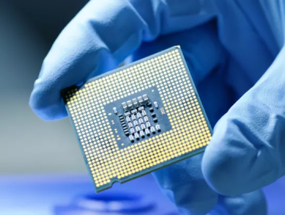
With artificial intelligence (AI) rapidly evolving, look for applications like voice recognition and image recognition to get more efficient, more affordable, and far more common in a variety of products over the next few years. This growth in applications will drive demand for new architectures that deliver the higher performance and lower power consumption required for widespread AI adoption. “The challenge for AI at the edge is to optimize the whole system-on-a-chip architecture and its components, all the way to semiconductor technology IP blocks, to process complex AI workloads quickly and at low power,” says Qualcomm Technologies Senior Director of Engineering Evgeni Gousev, who will provide an update on the progress of AI at the edge in a Data and AI program at SEMICON West, July 10-12 in San Francisco. Qualcomm Snapdragon 845 uses heterogeneous computing across the CPU, GPU, and DSP for power-efficient processing for constantly evolving AI models. Source: QualcommA system approach that optimizes across hardware, software, and algorithms is necessary to deliver the ultra-low power – to a sub 1-milliwatt level, low enough to enable always-on machine vision processing – for the usually energy-intensive AI computing. From the chip architecture perspective, processing AI workloads with the most appropriate engine, such as the CPU, GPU, and DSP with dedicated hardware acceleration, provides the best power efficiency – and flexibility for dealing with rapidly changing AI models and growing diversity of applications.“So far it’s been largely a brute force approach using conventional architectures and cloud-based infrastructure,” says Evgeni. “But we’re going to run out of brute force options, so future opportunities lie in developing innovative architectures, dedicated hardware, new algorithms, and new software. Innovation will be especially important for AI at the edge and applications requiring always-on functionality. Training is mostly in the cloud now, but in the near future it will start migrating to the device as the algorithms and hardware improve. AI at the edge will also remove some privacy concerns, an increasingly important issue for data collection and management.”Practical AI applications at the edge where resources are constrained run the gamut, spanning smartphones, drones, autonomous vehicles, virtual reality, augmented reality and smart home solutions such as connected cameras. “More AI on the edge will create a huge opportunity for the whole ecosystem – chip designers, semiconductor and device manufacturers, applications developers, and data and service providers. And it’s going to make a significant impact on the way we work, live, and interact with the world around us,” Evgeni said.Future generations of chips may need more disruptive systems-level change to handle high data volumes with low power A next-generation solution for handling the massive proliferation of AI data could be a nanotechnology system, such as the collaborative N3XT (Nano-Engineered Computing Systems Technology) project, led by H.S. Philip Wong and Subhasish Mitra at Stanford. “Even with next-generation scaling of transistors and new memory chips, the bottlenecks in moving data in and out of memory for processing will remain,” says Mitra, another speaker in the SEMICON West program. “The true benefits of nanotechnology will only come from new architectures enabled by nanosystems. One thing we are certain of is that massively more capable and more energy-efficient systems will be necessary for almost any future application, so we will need to think about system-level improvements.” Major improvement in handling high volumes of data with low high energy use will require system-level improvements, such as monolithic 3D integration of carbon nanotube transistors in the multi-campus N3XT chip research effort. Source: Stanford UniversityThat means carbon nanotube transistors for logic, high density non-volatile MRAM and ReRAM for memory, fine-grained monolithic 3D for integration, new architectures for computation immersed in memory, and new materials for heat removal. “The N3XT approach is key for the 1000X energy efficiency needed,” says Mitra.Researchers have demonstrated improvements in all these areas, including multiple hardware nanosystem prototypes targeting AI applications. The researchers have transferred multiple layers of as-grown carbon nanotubes to the target wafer to significantly improve CNT density and have also developed a low-power TiN/HfOx/Pt ReRAM. The low-temperature CNT and ReRAM processes enable multiple vertical layers to be grown on top of one another for ultra-dense and fine-grained monolithic 3D integration. Other speakers at the Data and AI TechXpot include Fram Akiki, VP Electronics, Siemens; Hariharan Ananthanarayanan, motion planning engineer, Osaro; and David Haynes, Sr. director, strategic marketing, Lam Research. See SEMICONWest.org.Paula Doe, SEMI
Read More