downloadGroupGroupnoun_press release_995423_000000 copyGroupnoun_Feed_96767_000000Group 19noun_pictures_1817522_000000Member company iconResource item iconStore item iconGroup 19Group 19noun_Photo_2085192_000000 Copynoun_presentation_2096081_000000Group 19Group Copy 7noun_webinar_692730_000000Path
Skip to main content
Default Banner Image

high-volume manufacturing

SEMI spoke with Eyal Shekel, senior vice president of Service Strategy and Excellence at Tokyo Electron Limited, about the impact of artificial intelligence (AI) on smart manufacturing and how other fab solutions for smarter process tools are advancing semiconductor manufacturing.Eyal shared his views ahead of his presentation at the SEMI Fab Management Forum, 17 February, as part of the SEMI Technology Unites Global Summit, 15-19 February 2021, an online event. Join us to meet experts from Tokyo Electron and other key industry influencers. Registration is open. SEMI: AI technology is considered a key enabler for smart manufacturing. What are the latest trends? Shekel: The advent of advanced nodes and extreme complex 3D semiconductor geometry has lengthened time to market and increased costs in areas ranging from equipment development and large-scale metrology usage to monitoring yield inhibitors.AI is becoming a critical tool in the area of material informatics to determine suitable materials and processing techniques in order to meet the needs of future devices. Together with new materials and processes, the development and implementation of virtual metrology will enable accurate and almost absolute real-time monitoring of our customers’ device wafers at each stage of the manufacturing process.SEMI: What are the benefits of data analysis in the process from R D and Ramp-Up to High-Volume Manufacturing? Shekel: The new research field of materials informatics enabled by AI provides tools to guide the highly efficient discovery and optimization of production processes. For example, TEL has developed methodologies for co-optimizing processes and materials for etch rates.To monitor and manage the yield of semiconductor fabrication processes, direct metrology measurements are important. However, it is difficult to monitor all production wafers due to the time and cost involved. With deep learning AI, it is now becoming possible to predict every wafer’s metrology measurements based on production equipment data and previously processed wafer metrology variables. This enables total quality management and run-to-run control, while simultaneously reducing production costs and cycle time.SEMI: Can you tell us more about TEL Service Advantage?Shekel: TEL Service Advantage is a TEL global support organization that allows customers to select a service plan that fits their needs. Through TEL Service Advantage, we can quickly respond to customer requests and technical advancements. TEL Service Advantage provides various plans to maximize equipment maintenance efficiency for customers and productivity from equipment manufactured by TEL. TEL Service Advantage plans can be combined to meet customer needs and achieve maximum results.A key enabling element of TEL Service Advantage is TELeMetrics™. TEL analyzes equipment data from various sensors using a remote connection and, based on that analysis, provides solutions to customer-specific problems around equipment throughput and predictive maintenance.SEMI: How is AI helping during the pandemic? Can you share a success story? Shekel: The pandemic forced severe travel restrictions worldwide, making it very difficult or even impossible in many cases to visit our customers, as it is still the case today. Standard communication devices like smartphones and email helped at the beginning when TEL intensified the remote support by our Total Support Centre (TSC).TEL continued to develop its Service Advantage program quickly, and started using additional advanced tools and methodologies such as the following: Deployed AR (Augmented Reality) to remotely assist our customer and TEL engineers Secured remote connections into TEL tools to investigate parameters and logs, or to change set-up Used remote training courses that connects trainers via video conferencing systems and training tools in the factories to skill up engineers located in a different parts of the world Used AR glasses for tool start-up and troubleshooting Expanded TEL database global technology with multi-tool on languages search capabilities A key project at a customer site in Europe offers an excellent success story. Using all the approaches above, we collaborated with the local team to put a tool into production with no major delays. This was highly appreciated by the customer and very important for us.SEMI: What do you predict for the future? Shekel: Global technology infrastructure continues to develop and expand rapidly. Elements like 5G networks, IoT and advanced sensing capabilities will lead to what we call General AI, which will be based on neuro-like infrastructure. The auto learning will spread across domains and rely on internal logic and reasoning to automate many tasks that are manual today. In our industry in particular, General AI will enable workers to focus more on data analytics and future advanced R D rather than ongoing operations.SEMI: How can technology unite us? What do you expect from your participation at SEMI Technology Unites Global Summit?Shekel: Technology united us in the last 150 years. The connectivity started with telegraph and telephone and was used to exchange information over wider distances. Nowadays, video conference capabilities, AR and improving communications technology makes it much easier to unite people who are geographically dispersed. This becomes obvious and valuable especially during this pandemic period. As a fact, we are able to continue to perform all our key activities – our tool support, training and customer relationships – even if we cannot be present in person.The SEMI Technology Unites Global Summit is a great chance to stay connected to people and customers that I would normally meet at the SEMICON exhibitions.It also offers the opportunity to network with many more people who I would not be able to meet otherwise. Moreover, I can watch speeches and presentations at any time! Normally I would miss some programs since exhibitions and events took place at the same time.Eyal Shekel, senior vice president of Service Strategy and Excellence at Tokyo Electron Europe Limited, is a 27-year semiconductor industry veteran. Upon his graduation as a Mechanical Engineer from the Technion (Israel leading technical institute), he joined Applied Materials. In 1997 he moved on to Tokyo Electron (TEL) in Europe, served as the Regional Service Manager of Israel and, soon after, was appointed the company’s General Manager. Since 2005 Eyal has been part of TEL Europe senior management. He oversaw the Service and Support Operations for TEL Europe as a senior vice president until 2019. In his current role, he co-leads TEL’s Global Service Committee in Japan.The SEMI SMART Manufacturing Initiative is a global effort to promote awareness of and interest in smart manufacturing with a focus on delivering industry-recognized best-in-class programs and services to enable members to maximize product quality and productivity while reducing costs. Activities are focused on building out core capabilities to enable smart manufacturing across the microelectronics supply chain. MADEin4 is a consortium of 47 partners from 10 countries connecting the full range of supply chain – from semiconductor equipment manufacturers and system-integrating metrology companies to RTOS and key applications such as the automotive industry. The MADEin4 Project develops next generation metrology tools, machine learning methods and applications in support of Industry 4.0 high-volume manufacturing in the semiconductor manufacturing industry. Serena Brischetto is senior manager of Marketing and Communications at SEMI Europe.
Read More
SEMI spoke with Thomas Fries, founder and CEO of FRT GmbH, about how hybrid metrology is shaping multi-sensor metrology tools to enhance measurement precision as the industry moves away from a single-sensor approach.Fries offered his views ahead of the SEMI MEMS Imaging Sensors Summit, 25 to 27 September 2019 in Grenoble, France. Join us at the event to meet experts from FRT Metrology and many other MEMS, imaging and sensors companies. Registration is open. SEMI: Metrology in front-end used to be straightforward. But then, as the number of tasks to be implemented increased, we moved to a multi-sensors approach. What drove this transition?Fries: I believe it´s more about software than about sensors. But of course the basis is the hardware. So, most metrology tools were designed around a specific sensor, e.g. a white light interferometer.A rigid frame, wafer fixtures, scanning tables etc. were then added to develop a complete system. In manufacturing more machinery was added, like handling systems, cleanroom equipment and more sensors, mainly for additive functions such as reading IDs or measuring temperature. The center was still the one and only sensor, being pimped more and more by some hardware features and a lot of software.SEMI: How are sensors and software shaping the way metrology is applied today?Fries: Today a huge number of optical sensors are available to provide various measurement options. But sometimes there are only very slight differences from one sensor to the other. A tiny variation may determine whether we solve a problem or end up fishing in troubled waters.And of course using different machines with those sensors requires high budgets for capital investment, used floor space, measuring time, etc. A multi-sensor platform solves all these problems. But again, it is the software that makes the real difference.SEMI: What lead to those advancements in metrology? What problems did they set out to solve?Fries: Metrology has been evolving ever since the measurement standards were established. The first challenge was to create a flexible mechanical platform that was also reliable and stable. All components were designed to be integrated into one system, mechanically, electrically and of course in the software.This level of integration requires not only an appropriate user interface, but also data formats and evaluation algorithms that leverage multi-sensor hardware. Today every metrology tool in the fab is justified by the application, not by specific sensors or specs. Of course the application leads to a set of specs, but the solution for the metrology task is realized within the software.New developments in metrology combine expertise in system design, physical knowledge in metrology and materials, mechanical engineering and also mathematical and software skills.The last step was the implementation of hybrid metrology functionality into a multi-sensor system that opens totally new doors in metrology. Before multi-sensors development, quite a few hitches could not be properly solved. SEMI: This is especially true when we consider applications in advanced packaging and MEMS manufacturing. What is in your opinion the main challenge?Fries: Specifically, in MEMS and advanced packaging we face multiple metrology challenges, as various processes run in one step and conditions on the wafer may vary quite often. In this case, a high degree of flexibility, up to the option to upgrade the metrology tool at any time or place, is a priceless advantage. Besides, cost effects for footprint, throughput and investment play a key role.A central task for nearly every customer application is to combine global measurements (complete wafer) and local measurements (per die) within one recipe. This is a perfect case for a multi-sensor platform. Measuring step heights and film thickness in one take is also an everyday routine. Combining those characteristics to measure hidden structures (hybrid metrology) is unique.SEMI: How will hybrid metrology enhance measurement precision and where do you expect the multi-sensor approach to be more applicable?Fries: The first advantage is the ability to measure properties that you cannot access directly. On top of that, all the previously mentioned features such as facing multiple metrology tasks, the combination of complete wafer and per die measurement are playing key roles. The precision of specific measuring tasks can be optimized by calibrating sensors against each other or combining results to get rid of noise or artefacts.MEMS and advanced packaging are natural playgrounds for hybrid metrology. But already today we see applications in high volume manufacturing in the 300mm fabs. As structures on wafers shrink, wafers are getting thinner and the whole process is becoming more and more complex. The classic one-sensor metrology tool is running out of gas. SEMI: What are your expectations regarding the summit in Grenoble, and for the future of the MEMS Sensors technology?Fries: FRT has always been very strong in MEMS and sensors and we have attended and exhibited at the SEMI MEMS Imaging Sensors Summit from the very beginning. The summit is always a very good meeting point for the community, and a perfect training session that gives participants extended updates in all fields. And of course, it grows our network and gives us the opportunity to show our latest products and applications.If you really want to know how the future of MEMS and sensors will look like, join the summit and don´t miss the chance to pass by the exhibition to meet FRT and many other industry leaders.Dr. Thomas Fries lives with his family close to Cologne. He is engaged in a variety of activities: as technical advisor to various ministries, supervisory board of PlanOptik AG, board and advisory board of IVAM, board member of COPT.NRW e. V., just to name a few. FRT supports many social projects as well as kindergartens and schools. Motorcycles and cars are still a great passion alongside his family.Serena Brischetto is senior marketing and communications manager at SEMI Europe.
Read More
SEMI met with Jay Zhang, business development director at Corning Incorporated, to discuss recent innovations at Corning that allow fine granularity CTE engineering as well as high Young’s modulus. We also talked about the impact of this work on in-process warp control, as well as the associated production methodology that provides rapid prototyping and high-volume manufacturing. We spoke ahead of his presentation at the 3D Systems Summit, 28-30 January, 2019, in Dresden, Germany. To register for the event, please click here.SEMI: What is Corning’s mission and vision and your role within the company?Zhang: Corning is one of the world’s leading innovators in materials science with a track record of 165+ years of life-changing innovations. We excel in glass science, ceramics science, and optical physics and succeed through sustained investment in RD E. Our products include Corning® Gorilla® glass, a durable material used on more than six billion mobile devices worldwide, and industry-leading LCD glass for display applications. We have recently dedicated a unit of the company called Precision Glass Solutions to address the emerging need for glass in the semiconductor industry. Here we apply Corning’s long history of glass science expertise and deep customer relationships in consumer electronics to support cutting-edge applications like wafer-level optics for precise 3D sensing and carrier solutions for temporary bonding applications in semiconductor manufacturing. It’s our most recent work in the Carrier Solutions product line that I’m excited to present: a new carrier glass product optimized for fan-out, called Corning Advanced Packaging Carriers.SEMI: What projects are you currently working on that you think will make a difference in 2019?Zhang: My team is excited to introduce Corning Advanced Packaging Carriers this year. This is a new line of product within our portfolio of Carrier Solutions. These ultra-flat glass carriers are specially developed to reduce customers’ challenge of in-process warp by up to 40 percent, which in turn helps advanced packaging customers achieve better yield.Corning Advanced Packaging Carriers feature high-stiffness properties and are available in a wide range of coefficients of thermal expansion (CTE) in fine granularity. These attributes help customers select an ideal glass carrier that will minimize in-process warp for their package. Furthermore, we make sample quantities of these carriers available in just four to six weeks to help maximize efficiency during customers’ R D process.My team is excited about the potential of this new product, but also encouraged by our results. We have already supplied this product and have heard from one of the largest semiconductor companies in Taiwan that it has reduced in-process warp by as much as 150μm.SEMI: Your presentation at the 3D Systems Summit will focus on Agile Manufacturing of Glass Carriers for Advanced Packaging. What exactly will you be sharing?Zhang: There is a lot of interest right now in using glass as a carrier substrate in temporary bonding applications in advanced semiconductor packaging – especially in fan-out processes. We also know that in-process warp is a significant challenge to companies pursuing advanced packaging because different CTE materials are added during the process. My team has done a lot of work to understand the impact that an ideal CTE glass carrier substrate can have on minimizing in-process warp. We have studied the available levers – both theoretical and in real-life fab environments – that can help address this challenge. I will present our findings on how it is possible to select a glass carrier with the ideal CTE and Young’s modulus to reduce in-process warp by up to 40 percent, and how Corning has developed an agile manufacturing platform to support customers with these ideal carriers from their R D stage through mass production.SEMI: What do you think will be a hot topic in the next few years?Zhang: We expect high-end fanout technology to address more applications beyond just mobile APs. There is also an interesting dynamic playing out between wafer-level and panel-level fan-out technologies. Corning is active in both areas. In developing and offering high performance glass carriers, we hope to help enable our customers to expand the fan-out applications space.SEMI: What are your expectations regarding the summit in Dresden, and why do you recommend your members and other industry leaders to attend the 2019 3D Systems Summit?Zhang: Europe is where some of the most advanced packaging technologies are born. Fan-out also saw early commercialization there. I hope to meet many scientists and technologists at 3D Systems Summit and exchange technical and business ideas. We also hope to get early feedback from other attendees about the value of our new product offering. Serena Brischetto is a marketing and communications manager at SEMI Europe.
Read More
Even for someone who has been in this industry since the days of the TI Datamath 4-function calculator and the TMS1100 4-bit microcontroller (yes, that’s been a LONG time – the movie Grease premiered the same year!), it is sometimes hard to grasp the scope and complexity of what happens in today’s leading-edge semiconductor gigafabs. In fact, the only way to comprehend the enormous volume of transactions that occur is to consider what happens in a single minute – this is illustrated in the infographic we have labeled “The Gigafab Minute.”* It’s amazing enough to think that a single factory can start 100,000 wafers every month on their cyclical journey through 1500 process steps… and have 99%+ of them emerge 4 months later to be delivered to packaging houses and then on to waiting customers. It’s quite another to realize that all of this happens continuously (24 x 7) and automatically. “How is this possible?” you ask.Well, a big part of the solution is the body of SEMI standards which have evolved since the early 80s to keep pace with the ever-changing demands of the industry. From an automation standpoint, many of these standards deal with the communications between manufacturing equipment and the factory information and control systems that are essential for managing these complex, hyper-competitive global enterprises.A significant characteristic of these standards is that they have been carefully designed to be “additive.” This means that new generations of SEMI’s communications standards do not supplant or obsolete the previous generations, but rather provide new capabilities in an incremental fashion. To appreciate the importance of this in actual practice, consider how the GEM, GEM300, and EDA/Interface A standards support the transactions that occur in a single Gigafab Minute.Starting at 1:00 o’clock on the infographic and moving clockwise, you first notice that 2.31 wafers enter the line. Of course, these are actually released in 25-wafer 300mm FOUPs (Front-Opening Unified Pod), but 100K wafers per month translates to 2.31 per minute. Since these factories run continuously, once the line is full, it stays full. And with an average total cycle time of 4 months, this means that there are 400K wafers of WIP (work in process) in he factory at any given time. This number, and the total number of equipment (5000+), drive the rest of the calculations.GEM (Generic Equipment Model) – SEMI E30, etc.The GEM messaging standards were initially defined in the early 90s to support the factory scheduling and dispatching applications that decide what lots should go to what equipment, the automated material handling systems that deliver and pick-up material to/from the equipment accordingly, the recipe management systems that ensure each process step is executed properly, and the MES (Manufacturing Execution System) transactions that maintain the fidelity of the factory system’s “digital twin.”Every minute of every day, GEM messages support and chronicle the following activities: 240 process steps are completed (i.e., 240 25-wafer lots are processed), 300 recipes are downloaded along with a set of run-specific adjustable control parameters, and 600 FOUPs are moved from one place to another (equipment, stockers, under-track storage, etc.). For each of these activities, the factory’s MES is notified instantaneously.GEM300 – SEMI E40, E87, E90, E94, E157With the advent of 300mm manufacturing in the mid-to-late 90s, a global team of volunteer system engineers from the leading chip makers defined the GEM300 standards to support fully automated manufacturing operations. Starting at 5:00 o’clock on the infographic, the number of transactions per minute jumps almost 3 orders of magnitude, from the monitoring of 900 control jobs across 4000 process tools to the tracking of 360,000 individual recipe step change events. This level of event granularity is essential for the latest generation of FDC (Fault Detection and Classification) applications, because precise data framing is a key prerequisite for minimizing the false alarm rate while still preventing serious process excursions. In this context, more than 6000 recipe-, product- and chamber-specific fault models may be evaluated every minute.Simultaneously, the applications that monitor instantaneous throughput to prevent “productivity excursions” and identify systemic “wait time waste” situations depend on detailed intra-tool wafer movement events. In a fab with hundreds of multi-chamber, single-wafer processes, 75,000 or more of these events occur every minute. EDA (Equipment Data Acquisition) – SEMI E120, E125, E132, E134, E164, etc.Rounding out the SEMI standards in our example gigafab is the suite of EDA standards which complement the command and control functions of GEM/GEM300 with flexible, high-performance, model-based data collection. The EDA standards enable the on-demand collection of the volume and variety of “big data” required from the equipment to support the advanced analysis, machine learning, and other AI (Artificial Intelligence) applications that are becoming increasingly prevalent in leading semiconductor manufacturers. As EUV (Extreme Ultraviolet) lithography moves from pilot production to high-volume manufacturing at the 7nm process node and beyond, the litho process area will become a major source of process data by itself, generating 10 GB of data every minute. This is in addition to the 100 GB of data collected from other process areas. The End ResultThe final wedge (12:00 o’clock) in our infographic highlights the real objective – which is producing the millions of integrated circuits that fuel our global economy and provide the technologies that are an integral part of our modern way of life. Assuming a nominal die size of 50 square mm (typical of an 8 GB DRAM), the 2.31 wafers we started at 1:00 o’clock result in almost 3200 individual chips. But none of this would be possible without the pervasive factory automation technology we now take for granted. So, as you finish reading this posting on whatever device you happen to be using, take a micro-moment to acknowledge and thank the hundreds of standards volunteers whose insights and efforts made this a reality!You may not be responsible for running a gigafab anytime soon, but the SEMI standards used in this setting are no less applicable to any Smart Manufacturing environment. Give us a call if you’d like to know more about how these technologies can benefit your operations for many years to come.Alan Weber is Vice President, New Product Innovations, at Cimetrix Incorporated. Previously he served on the Board of Directors for eight years before joining the company as a full-time employee in 2011. Alan has been a part of the semiconductor and manufacturing automation industries for over 40 years. He holds bachelor’s and master’s degrees in Electrical Engineering from Rice University. For more information on SEMI Standards, please click here.
Read More
Process power and reactive gas subsystems for semiconductor manufacturing equipment have grown at a CAGR of 21% since 2013. The segment growth is considerably above the critical subsystems industry average of 9.5% and is attributable to higher demand for vacuum processing equipment over the period.Process power and reactive gas subsystems now account for approximately 12% of all expenditures on critical subsystems used on semiconductor manufacturing equipment, up from 7% in 2013. The main driver of this exceptional growth has been the rise in vacuum processing steps (deposition and etch) during the manufacturing processes of both logic and memory devices. Most deposition and etch processes require an RF generator to provide a plasma energy source in the chamber, increasing demand for tools with power subsystems such as RF power supplies and matching networks.Multiple patterning and the advent of 3D NAND in high-volume manufacturing have significantly increased the number of deposition and etch processing steps and, in the case of 3D NAND, longer and more difficult etch processes are requiring a wider range of power solutions. Further analysis shows that 3D NAND has been the principle growth catalyst, with the total share of power subsystems going to memory applications increasing 8 percentage points since 2013. Memory applications now account for almost half of all power subsystems demand in 2018. Interestingly, investigation of power subsystems by tool type reveals that a clear majority of power subsystems (60%) find their way on to etch tools with only 40% on deposition tools. This can be explained by the fact that more delicate etch processes can require multiple RF power solutions per tool, whereas deposition does always use plasma energy sources, for example in thermal deposition processes.Despite the staggering growth performance of the power subsystems segment over the past five years, we expect the growth rate to moderate significantly in the run-up to 2023. Now that 3D NAND has been adopted in high-volume manufacturing, we expect the rate of increase in vacuum/plasma processing steps to slow down. The introduction of EUV also has the potential to taper demand for vacuum processing equipment. However, it is not expected the reverse the trend as multiple patterning techniques will still be needed in conjunction with EUV to achieve the desired improvements in device density and performance. The future growth trend for power and reactive gas subsystems is forecast to be in line with the critical subsystems industry average at approximately 2.0% CAGR until 2023.For more information about Critical Subsystems and VLSI Research, please visit www.vlsiresearch.com/public/csubsJulian West is a technical and market analyst at VLSI Research Europe.
Read More
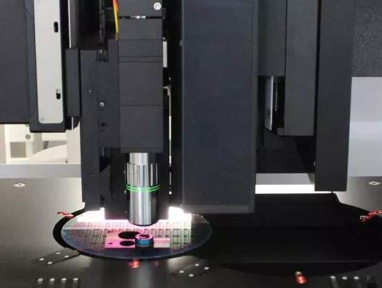
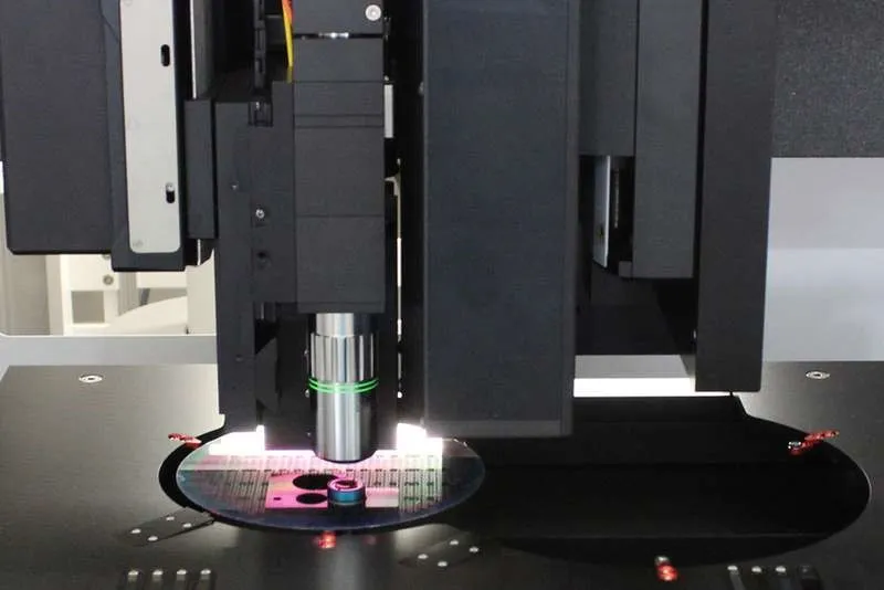
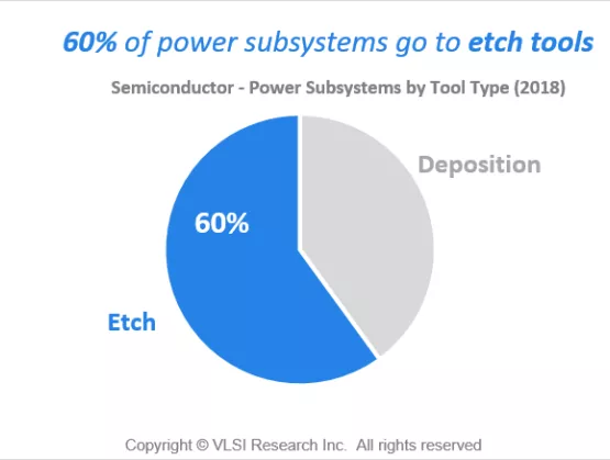
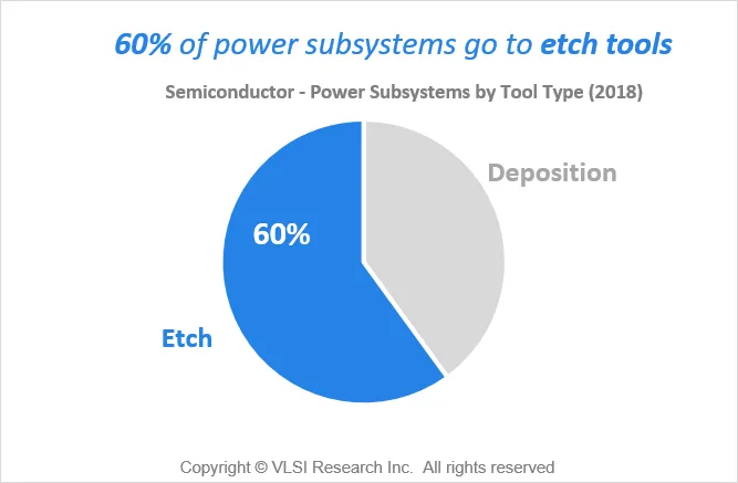
The Advanced Lithography TechXPOT at this year’s SEMICON West will explore progress in extreme ultraviolet lithography (EUVL), its economic viability for high-volume manufacturing (HVM) and other lithography solutions that will address the march to 5nm and onward to 3nm.As a prelude to the event, SEMI asked Neeraj Khanna, Global Head of the Patterning Customer Engagement Team at KLA-Tencor, a speaker at the TechXPOT, for insights about the readiness of inspection and metrology tools for EUVL applications at 5nm and 3nm. For a full list of speakers and program agenda, visit http://www.semiconwest.org/programs-catalog/lithography-5nm-and-below.Neeraj Khanna, Global Head of the Patterning Customer Engagement Team at KLA-TencorSEMI: In general, how would you characterize the readiness of inspection and metrology tools intended for EUVL applications at 5nm and 3nm? In particular, what are some of the remaining research and development challenges that need to be addressed for each of these nodes?Neeraj Khanna: KLA-Tencor is working closely with its customers to qualify and ramp EUV. Our suite of inspection, metrology and data analytic solutions are being implemented to enable EUV infrastructure readiness including, for example, new reticle and resist qualification, scanner qualification, and EUV ramp preparation. These EUV integration activities require process control systems that support a wide range of applications, including hotspot discovery, lithography modeling, focus/dose process window qualification, reticle print check, mask blank inspection, and process and tool monitoring.As with any major technology inflection, it is critical to understand sources of process variation to enable ramp at optimal yield. For example, stochastics result in random pattern variations, which have a major impact on EUV yield. To manage stochastics, IC manufacturers are deploying process control solutions that support fast modeling of stochastic variations coupled with high-sensitivity, high-coverage wafer defect inspection. Another example is a methodology called hybrid scanner utilization whereby, when EUV scanners are implemented in production, they will only be used for a few layers, while all other layers will be patterned with 193i scanners. This technique requires tighter control and monitoring of overlay budgets.SEMI: How are you able to achieve this tighter control and monitoring?NK: To understand why hybrid scanner utilization requires tighter control and monitoring of overlay budgets, it’s important to outline how this differs from current scanner implementation. For critical layers in current process flows using 193i lithography, pattern layers for a given wafer are printed using the same stage/chuck on the same scanner. The overlay performance achieved using this lithography strategy is called dedicated chuck overlay (DCO). Use of a dedicated scanner and chuck for lithography reduces inter-scanner and inter-chuck distortion effects, resulting in DCO overlay error of less than 1nm. When EUVL is first implemented in production, it will be used for a few layers – likely, cut masks and contacts with eventual migration to metal 1 layers. All other layers will be patterned with 193i scanners. This hybrid scanner operation eliminates any possibility of using a dedicated scanner and dedicated chuck to support tight overlay performance specifications. Instead, fabs will be forced to optimize mix-and-match overlay (MMO), with the overlay performance obtained using different scanners for printing different layers on a given wafer.With overlay specifications for advanced DRAM and logic at ~2.5nm, fabs will need to implement strict 193i-to-EUV scanner matching strategies or risk consuming 60 to100 percent of the overlay budget on just MMO. To achieve tighter overlay control and monitoring required for MMO, fabs need to implement dense, in-field overlay error measurements that feed into scanner fleet management systems. KLA-Tencor’s ATL™ overlay metrology system supports a high measurement speed and the use of small in-die targets, enabling dense in-field overlay measurements with high accuracy. Our 5D Analyzer® data analytic and management system includes scanner fleet management capability that enables automatic product-based corrections to minimize MMO error, helping fabs reduce the risk to yield loss associated with a 193i-EUV mixed scanner implementation. SEMI: What other challenges do you see coming to the fore at 5nm and 3nm?NK: Overall, the 5nm and beyond design nodes will face challenges associated with new lithography technology, potential new device structures and smaller pattern pitches. IC manufacturers will require process control solutions that not only identify process windows, but also monitor patterning parameters and defectivity at multiple points to identify process shifts. To monitor dynamic processes at these advanced nodes, inspection and metrology tools will need to have both sensitivity to critical parameters/defects and robustness to process variation in order to provide IC engineers with smart feedback for efficient control of their processes.SEMI: Could you elaborate on what will be required to monitor patterning parameters and defectivity at multiple points? How different will the techniques be at 5nm/3nm vs. at say, 7nm or 10nm?NK: As an example of monitoring at multiple points, consider the transition to EUV lithography. With EUV, the cost per scan goes up dramatically. Thus, IC manufacturers will monitor parameters at multiple points to maximize yield and minimize risk: EUV reticle qualification requires inspection and metrology throughout the entire flow from mask blank manufacturing, to the mask shop, to the IC fab. For the advanced design nodes associated with EUV, wafer qualification requires monitoring and control of wafer defectivity, shape and geometry throughout the wafer manufacturing process. It also requires control of fab incoming wafer qualification while ensuring that fab-wide processes are meeting defect and shape standards necessary for printing smaller feature sizes. EUV resist characterization and qualification requires comprehensive lithography simulation, wafer defect inspection, and film thickness and uniformity measurements to help reduce development time and prepare the litho stacks for production ramp. As EUV scanners are ramping, fabs are faced with finding any unknown particle sources within the new scanner chambers. This situation is driving the need for tighter and more frequent PWP (particles per wafer pass) chamber monitors to ensure scanner cleanliness. In addition, EUV scanner qualification requires reticle front and backside particle checks, and hotspot discovery and process window qualification using optical wafer defect inspection and e-beam review. EUV process monitoring encompasses overlay error monitoring, focus/dose monitoring, critical dimension (CD) and 3D device shape monitoring, and continuous process window monitoring. EUV inline defect monitoring and tool monitoring is important for reducing baseline defectivity in the litho cell for faster ramp, and for early identification of litho excursions in production. A critical part of this monitoring strategy is inline after develop inspection (ADI) monitoring, which is defect inspection on patterned wafers after printing and development of the resist ADI. Inline ADI innovations that find yield-critical defects allow fabs to reduce process issues, prevent at-risk wafers early in the process, and enable rework when excursions are found in production. As with past technology transitions, the implementation of multiple monitoring steps as part of a comprehensive process control strategy will be critical for a fab’s successful ramp of EUV.Debra Vogler, SEMI
Read More