downloadGroupGroupnoun_press release_995423_000000 copyGroupnoun_Feed_96767_000000Group 19noun_pictures_1817522_000000Member company iconResource item iconStore item iconGroup 19Group 19noun_Photo_2085192_000000 Copynoun_presentation_2096081_000000Group 19Group Copy 7noun_webinar_692730_000000Path
Skip to main content
Default Banner Image

Siemens

The automation of semiconductor factories through digitization is reshaping Smart Manufacturing to streamline the connectivity and orchestration of manufacturing processes across the entire supply chain. But the threat of cyberattacks and viruses looms. An estimated 26 billion smart and connected manufacturing devices are expected to be online by next year. Never before has the need been greater to protect the staggering volume of manufacturing data traversing increasingly intricate supply chain networks.“We are living in the time of digital manufacturing,” said Chen Chi-Hsien, Director of TSMC’s Manufacturing Technology Center. “Processes ranging from assembling equipment and upgrading hardware and software are increasing security challenges for semiconductor manufacturers. With viruses and malware constantly evolving to pose greater threats, all members of the supply chain – from manufacturing and equipment to operating system and software/firmware providers – should work together within the SEMI Smart Manufacturing platform to establish cybersecurity standards across the industry. Doing so will also enhance the development of smart manufacturing and accelerate digitalization.” Representatives from Tongfu Microelectronics, Adlink, NSHC, ABB, TSMC, ASE and Microsoft with SEMI CMO and SEMI Taiwan president Terry Tsao (left to right) Chi-Hsien offered his insights at the SEMI Smart Manufacturing and Cybersecurity Seminar, joining speakers from other leading semiconductor manufacturers including TFME and ASE to discuss the latest smart manufacturing trends and cybersecurity challenges. The April event in Hsinchu also featured representatives from ABB, Adlink, Microsoft, Rockwell, Siemens, Delta Electronics and the National Center for High-Performance Computing (NCHC) offering their views on how the semiconductor industry can speed its digital transformation using various technologies.With its 43 years’ experience in developing international standards, SEMI is committed to serving as the platform to establish universal information security standards for silicon wafer plants and semiconductor equipment, Terry Tsao, SEMI chief marketing officer and SEMI Taiwan president, said at the seminar. Tsao added that SEMI is now in discussions with leading semiconductor manufacturers to establish a communications framework for addressing potential security risks and facilitating the development of risk management and security solutions that safeguard the semiconductor supply chain.This year SEMI will debut its SMART Manufacturing EXPO to gather key supply chain players for critical discussions about security and to feature AI manufacturing and cybersecurity solutions. Co-located with SEMICON Taiwan, September 18-20, 2019, at TaiNEX 1 (Taipei Nangang Exhibition Center, Hall 1), the SMART Manufacturing EXPO will include Smart manufacturing hardware and software providers from around the world for the interdisciplinary discussions and collaboration key to developing strong Smart manufacturing security.For more information about the SEMI Smart Manufacturing Platform, contact Emmy Yi of SEMI Taiwan at [email protected] Yi is a marketing specialist at SEMI Taiwan.
Read More
Creating a custom Internet of Things (IoT) IC is challenging because it involves multiple design domains (digital, analog and RF). Creating a sensor-based IC that combines electronics that use the traditional CMOS IC design flow with a MEMS sensor on the same silicon die, however, can seem impossible. Couple the co-design and verification challenges with a lack of traditional process design kit (PDK) support for MEMS, and you have a tough road to travel to get your IoT designs to market.What can we do to make the sensor-based IoT design community successful?Understanding the ChallengesThe sensor-based IoT IC typically features a MEMS sensor (and optional actuator) that interact with the real world. Analog and digital circuitry processes the signals and sends them to a CPU. The CPU provides the “smarts” to process the data from the sensor and then sends processed data via a radio to the Internet; alternatively, the CPU could activate the actuator. A typical sensor-based IoT IC (Source: Mentor: A Siemens Business) Based on the complexity of the system, designers face many co-design challenges: Analog design requirements imposed by MEMS: MEMS devices often require high voltages and multiple power supplies; they emit small signals that need amplification and conditioning; and they are sensitive to the environment and require calibration. Design flow interactions: Parasitics from MEMS devices might affect circuits and vice versa. Circuit designers need MEMS models for impedance and timing. Integration: MEMS devices operate at different timescales than circuits, which adds a layer of complexity. Compounding the problem is a lack of MEMS PDKs and methods to tie together ICs and MEMS PDKs for integration and cross-verification. After conquering the co-design challenges, the design team has to address mixed-domain simulation challenges that include: Simulating the system: This requires verification of MEMS, digital, analog and RF circuitry with embedded software that runs on the CPU. Timescales: These vary widely, from a single deflection of the MEMS transducer in femtoseconds to a seconds-long simulation of the embedded software performing a measurement and transmitting data. Simulation time: Simulation of a behavioral digital design is extremely fast. However, the system simulation requires stand-in models that incorporate the behavior of the analog and MEMS block to simulate in an acceptable amount of time. The challenge of timescales for co-simulation. (Source: Mentor: A Siemens Business) MEMS is the KeyThe reality is that it’s the MEMS device that adds extra complexity to the sensor-based IC design and verification flow. To amplify the problem, the MEMS manufacturing process is not nearly as mature as the standardized IC process. For example, the standardized IC process includes ready-made PDKs that include everything designers need to move through design and verification flows. Foundries often provide soft and hard IP to quickly build-out design, and EDA tools provide high levels of automation enabled by abstraction and a standardized IC flow. How will MEMS-based design evolve?MEMS-based design must catch up to the standardized IC process. The first step is providing MEMS PDKs that include: Multi-physics domain design rules and material properties Packaging information Wafer and bonding information Fabrication information We must also tackle issues associated with these PDKs, including: Ownership, distribution and maintenance of the PDKs Consensus on the contents of the PDKs Merging of CMOS and MEMS PDKs The industry needs to move toward standardized MEMS manufacturing processes with available PDKs. Companies must provide IP and recommend structured design methods for co-design and verification of ICs that incorporate MEMS. How can EDA help with these flows?The EDA ContributionEDA companies must work with teams in the MEMS IC co-design space, collaborating with MEMS fabricators to help enable PDKs. By incorporating PDK support within their own tools, EDA companies can provide an integrated custom IC flow that allows teams to design and verify MEMS-based ICs. For details about this flow, click here to download the Mentor whitepaper: Fusing CMOS IC and MEMS Design for IoT Edge Devices.Greg Lebsack brings 25 years of executive and technical management experience — along with a proven track record of building strong teams and delivering predictable results — to his role as general manager of the ICDS division of Mentor, a Siemens Business. Lebsack joined Mentor in 2015 after that company acquired Tanner EDA, where he was president. Prior to Tanner EDA, he held management and technical positions in a number of different industries and companies, including Sprint, General Electric and McKinsey Co. Greg holds a bachelor’s degree in business administration from Northern Arizona University.Greg Lebsack recently presented on the topic of Integrated Co-design of MEMS/IC at the MEMS Sensors Technical congress, a technical conference organized by the MEMS Sensors Industry Group.
Read More
Five young dancers bathed in a striking rainbow of colors with their silhouettes cast in the background dazzled SEMICON Japan 2018 attendees at the opening ceremony in mid-December. Gone were the standard opening keynotes and ribbon cutting, replaced by live performance and media art set against a dramatic black backdrop. There was no mistaking the wide-eyed looks of wonder in the audience.In its sheer vibrance, the opening ceremony thrilled with an excitement that seemed to embody the extraordinary growth expectations for the global semiconductor supply chain over the next five years, with the industry poised to double sales from $2 trillion to a staggering $4 trillion – a phenomena SEMI president and CEO Ajit Manocha has called The Rebirth of the Semiconductor Industry. Driving this unprecedented growth will be SMART applications that are transforming industries and applications worldwide, powered by artificial intelligence (AI) and Internet of Things (IoT) technologies.The dramatic scene at SEMICON Japan 2018 was staged by Rhizomatiks, a media arts company that produced the Rio Olympic Games closing ceremony and is famous for its pop music spectacles. The company’s CTO, Motoi Ishibashi, the event’s first keynote speaker, described his team’s development of drones and vehicles guided by motion and precision-control technologies. It was some of these SMART vehicles that maneuvered the opening ceremony performers from the dance company Elevenplay onstage. Only Rhizomatiks, Ishibashi said, has this capability. In its mission to enrich people’s lives through new media arts, Rhizomatiks uses the latest virtual and mixed-reality technologies to orchestrate not only dance performances but music videos, commercials, fashion shows and festivals.Toru Nishikawa, the second keynote speaker and CEO at Preferred Networks, a leading Japan-based developer of deep learning software programs, surprised the SEMICON Japan audience with his discussion of his company’s work to develop a specialized chip for deep learning processing, joining technology giants Apple, Google, Alibaba and Microsoft in chip design. As more IT and software companies develop specialized, differentiated chips, the devices are quickly becoming the heartbeat of SMART technologies. The company’s approach has taken hold. Only four years old, Preferred Networks is enjoying rapid growth by working with global powerhouses including Toyota, NTT, Panasonic, Fanuc, NVIDIA, Intel and Microsoft. Ishibashi’s and Nishikawa’s fresh visions and the media arts extravaganza reflected the success of SEMICON Japan, held again at Tokyo Big Sight: The event’s 1,881 booths – filled by 727 exhibitors from 14 regions – was the highest count in six years. With Japan home to companies that supply about 40 percent of semiconductor equipment and materials worldwide, top suppliers historically have occupied the largest spaces on the SEMICON Japan show floor.According to IDC, personal computers and smartphones, long the largest revenue sources for the semiconductor industry, will remain top revenue drivers in the coming years. But revenue from new SMART technologies for applications such as automotive and factory automation is growing, a trend expected to continue with a 2018-2022 CAGR of 9.5 percent for automotive and 5.2 percent for manufacturing, compared to 1.1 percent for PCs and 2.9 percent for smartphones.SEMICON Japan’s new SMART Applications zone highlighted these and other new market opportunities for semiconductor growth with product and technology exhibits from companies including Bosch, IBM, Microsoft, NEC, Preferred Networks, Sony, SAS, Siemens, Tesla and Toyota. But the zone wasn’t all work and no play. The ROBOT SQUARE and SPORTS x IOT robot exhibits took visitors back to their school days, with robot anime – from Astro Boy to Gundam and Evangelion – that they could ride and control! As the World Gets Smarter, So Must SEMICON and the IndustryWe all agree the world is getting smarter at a fast pace. New cars are easier to drive – some models are almost fully autonomous on highways and streets. Your SMART speaker has gone well beyond an audio playback device and is more like a home AI platform. Almost all storefronts are equipped with video cameras. Your workplace, whether an office or a factory, is driven by automation. The reliance of these environments and devices on semiconductors is driving exponential chip and changing the world. Businesses need to adapt and so do SEMICON events. We’re doing just that as SEMICON Japan 2018 demonstrated – from an opening ceremony enabled by technology innovation to new faces of the industry to the SMART Application zone. As the SEMICON Japan presidents’ reception concluded the first day of the show, a robot from the ROBOT SQUARE suddenly appeared in the reception hall in front of about 250 executives from the global industry. Everyone at the reception was impressed and stepped forward to the stage, reflecting the overall excitement about SEMICON Japan, which for many years showcased only chip manufacturing equipment and materials. This year, to keep pace with the changing world, it was much more than that.SEMICON Japan 2019 will again take place in December at Tokyo Big Sight. However, organizers of the Tokyo Olympics will be using the East Exhibit Hall usually occupied by SEMICON Japan to prepare for the games. As a result, SEMICON Japan will be held in the West and South Halls instead. Look for more changes to the event. I hope to see you next year!Jim Hamajima is president of SEMI Japan.
Read More
What’s next for smarter, more connected electronics manufacturing - Part 3 The fast-maturing infrastructure now enabling analysis of exponentially larger data volumes brings the microelectronics industry to an inflection point, where the winning companies will be the first to master the use of this data to solve the industry’s emerging challenges. SEMI expands its coverage of these vital issues with a Smart Manufacturing Pavilion and three days of talks SEMICON West, July 10-12 in San Francisco. 
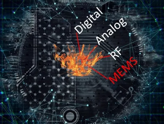
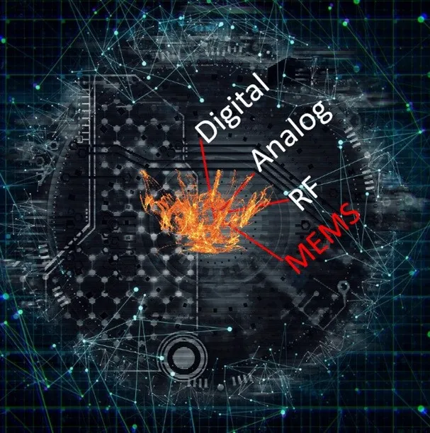
While deep learning is starting to be applied to image recognition for wafer inspection, it is also being considered for sequential pattern recognition in order to evaluate equipment parameter traces. The next emerging applications will start to use those learned patterns to predict outcomes, and then use those predictions to automate process control. One early application of deep learning is IC process development. “People don’t think of research and development as the first place to automate, but it’s where applying our digitization and simulation has first had impact,” says David Fried, Coventor vice president of Computational Products. He noted that insertion is easier in the lab than in the fab. Technology at 10nm and beyond is now so complex that companies at the leading edge must use process modeling to understand the effect of process variation on their designs. Learning cycles can now be accelerated during development by simulating 10,000 digital wafers instead of running 25 actual wafers during screening, Fried says. Applying structured analysis and machine learning to the data simplifies optimization across the 500 or more interrelated process steps. Coventor has recently introduced a statistical analysis package that aids the design and analysis of process variation experiments by using large volumes of data from its models. Fried says these models are next being used to accelerate the yield ramp in manufacturing. Digital simulation also could speed development of high-mix, lower value products While digital twins are best known for their use in complex, high value products like jet engines, the simulation technology could also enable the electronic manufacturing services (EMS) sector to reduce the time, cost and risk of developing its high mix of products. “The EMS sector’s use of digital twins will be vital for it to smooth the move of CAD/CAM digital design data for so many different products into manufacturing, and to accelerate validation testing of designs and products by doing more of it in the virtual world,” says Dan Gamota, vice president of Engineering and Technical Services at Jabil. Gamota also highlights the push for traceability from the automotive and healthcare markets, where the digital models could be used to quickly assure that the design was built exactly as specified. “In the past year, traceability has evolved from just ‘nice to have’ to ‘how to achieve,’” he adds. “Companies are expecting it, but aren’t willing to accept the cost and risk of doing it alone. We need the community to discuss realistic implementations, identify the most critical elements and bring together the ecosystem partners to build baseline reference architectures for key digital building blocks. The community also needs to assure the reliable flow of data among the electronic manufacturing segments from semiconductor to OSAT to EMS.” Predictive maintenance and virtual metrology applications could mature in next few years While predictive maintenance initially seemed a likely early application of machine learning in factories, it remains a challenge for the electronics sector. “The difficulty is that it’s not clear where to get the most bang for the buck,” says Tom Ho, president of BISTel America, noting that it may make the most sense to track the failure performance of a single expensive part, like an electrostatic chuck, since predicting the failure performance of a whole complex system like an etcher is much harder. “Collecting enough data from all failure types, including especially the rare events, is difficult unless you have a long history of a lot of tools,” adds Doug Suerich, PEER Group product evangelist. “The gain from collecting performance information from many tools across the industry could be big, but many companies still need to overcome concerns around exposing their IP.” Another big opportunity for prediction is virtual metrology – predicting the wafer outcome from the process or sensor data with enough accuracy to replace the physical metrology. “Virtual metrology is improving, and since metrology can be slow and expensive, any reduction could mean a huge potential savings,” says Suerich. “But it is still seen as too scary for many companies. Two to three years from now, companies will expand the practice from lower risk areas into processes that require more confidence in the results.” Moving beyond prediction to automated control needs digital models Once the results are predicted, the model can be used to control or automatically optimize a process and enable the system to learn by itself, usually by reinforcement learning on a digital model. The model can then independently make adjustments to optimize the manufacturing process. “Automated process development is getting close now. Instead of smart guys turning the knobs, deep learning is automating the smart tuning,” says Suerich, suggesting the industry could see widespread adoption in as little as two to three years. This type of machine learning needs a good digital model, and masses of data for learning. One approach uses human experts to build a physics-based model of the clearly understood parts of the process, then turns to deep machine learning to optimize the lesser-understood variables. The alternative, the data-first approach, runs a computer algorithm to suggest the solution purely from data, without human input, and then relies on the human to evaluate the usefulness of the results. Modeling digital twins of wafers could enable automated process control, chamber matching, and fleet matching, says Fried. If every wafer had its own virtual twin with all the upstream metrology and structural information needed to make equipment control decisions, it could feed forward that information to enable the seamless transition from one step in the process to another based on understanding their complex interrelationships. This could potentially improve uniformity across wafers and equipment, and reduce the need for metrology, he argues. Moving metrology sensors into the chamber will also require model-based algorithms to enable dynamic process control in close to real time, says Fried. These algorithms will be needed to acquire, parse, and process the data at high speed, and then to choose how to adjust the controls. “There will be a model behind collecting and interpreting the metrology data,” he notes. “That’s a really rich vein for improvements in process control.” “The end goal is to collect equipment data in real time, analyze it with AI, and send back controls to optimize manufacturing processes,” Jabil’s Gamota says. “This requires a robust architecture for communication between equipment and consistent formats for data collection and analysis. But the cost and complexity of this heavy lifting is too great for any one company to do alone. We need a consensus-based architecture for ingesting, analyzing and acting on the data.” SEMI tests data transfer protocols, benchmarks best practices SEMI is launching a smart data project to identify the various data transfer protocols needed for inter-company communications. The project will feature a proof-of-concept model in a development fab to produce verifiable results so SEMI can better understand how different approaches meet member needs. SEMI’s smart manufacturing technology communities and the Fab Owners Alliance are also benchmarking current smart manufacturing practices in the microelectronics industry to help SEMI members better understand the path forward and potential return on investment. Speakers over all three days at SEMICON West addressing these issues include Active Layer Parametrics, Applied Materials, Applied Research Photonics, ASML, Bosch Rexroth, Cimetrix, Coventor, ECI Technologies, Edwards Vacuum, Final Phase Systems, GE Digital, Infineon, Jabil, Lam Research, Osaro, Otosense, PEER Group, Qualcomm, Rockwell Automation, Rudolph Technologies, Schneider Electric, Seagate, Siemens, Stanford University, TEL, TIBCO Software. See semiconwest.org. What’s next for smarter, more connected electronics manufacturing - Part 1 What’s next for smarter, more connected electronics manufacturing - Part 2 Paula Doe, SEMI
Read More
With artificial intelligence (AI) rapidly evolving, look for applications like voice recognition and image recognition to get more efficient, more affordable, and far more common in a variety of products over the next few years. This growth in applications will drive demand for new architectures that deliver the higher performance and lower power consumption required for widespread AI adoption. “The challenge for AI at the edge is to optimize the whole system-on-a-chip architecture and its components, all the way to semiconductor technology IP blocks, to process complex AI workloads quickly and at low power,” says Qualcomm Technologies Senior Director of Engineering Evgeni Gousev, who will provide an update on the progress of AI at the edge in a Data and AI program at SEMICON West, July 10-12 in San Francisco. Qualcomm Snapdragon 845 uses heterogeneous computing across the CPU, GPU, and DSP for power-efficient processing for constantly evolving AI models. Source: QualcommA system approach that optimizes across hardware, software, and algorithms is necessary to deliver the ultra-low power – to a sub 1-milliwatt level, low enough to enable always-on machine vision processing – for the usually energy-intensive AI computing. From the chip architecture perspective, processing AI workloads with the most appropriate engine, such as the CPU, GPU, and DSP with dedicated hardware acceleration, provides the best power efficiency – and flexibility for dealing with rapidly changing AI models and growing diversity of applications.“So far it’s been largely a brute force approach using conventional architectures and cloud-based infrastructure,” says Evgeni. “But we’re going to run out of brute force options, so future opportunities lie in developing innovative architectures, dedicated hardware, new algorithms, and new software. Innovation will be especially important for AI at the edge and applications requiring always-on functionality. Training is mostly in the cloud now, but in the near future it will start migrating to the device as the algorithms and hardware improve. AI at the edge will also remove some privacy concerns, an increasingly important issue for data collection and management.”Practical AI applications at the edge where resources are constrained run the gamut, spanning smartphones, drones, autonomous vehicles, virtual reality, augmented reality and smart home solutions such as connected cameras. “More AI on the edge will create a huge opportunity for the whole ecosystem – chip designers, semiconductor and device manufacturers, applications developers, and data and service providers. And it’s going to make a significant impact on the way we work, live, and interact with the world around us,” Evgeni said.Future generations of chips may need more disruptive systems-level change to handle high data volumes with low power A next-generation solution for handling the massive proliferation of AI data could be a nanotechnology system, such as the collaborative N3XT (Nano-Engineered Computing Systems Technology) project, led by H.S. Philip Wong and Subhasish Mitra at Stanford. “Even with next-generation scaling of transistors and new memory chips, the bottlenecks in moving data in and out of memory for processing will remain,” says Mitra, another speaker in the SEMICON West program. “The true benefits of nanotechnology will only come from new architectures enabled by nanosystems. One thing we are certain of is that massively more capable and more energy-efficient systems will be necessary for almost any future application, so we will need to think about system-level improvements.” Major improvement in handling high volumes of data with low high energy use will require system-level improvements, such as monolithic 3D integration of carbon nanotube transistors in the multi-campus N3XT chip research effort. Source: Stanford UniversityThat means carbon nanotube transistors for logic, high density non-volatile MRAM and ReRAM for memory, fine-grained monolithic 3D for integration, new architectures for computation immersed in memory, and new materials for heat removal. “The N3XT approach is key for the 1000X energy efficiency needed,” says Mitra.Researchers have demonstrated improvements in all these areas, including multiple hardware nanosystem prototypes targeting AI applications. The researchers have transferred multiple layers of as-grown carbon nanotubes to the target wafer to significantly improve CNT density and have also developed a low-power TiN/HfOx/Pt ReRAM. The low-temperature CNT and ReRAM processes enable multiple vertical layers to be grown on top of one another for ultra-dense and fine-grained monolithic 3D integration. Other speakers at the Data and AI TechXpot include Fram Akiki, VP Electronics, Siemens; Hariharan Ananthanarayanan, motion planning engineer, Osaro; and David Haynes, Sr. director, strategic marketing, Lam Research. See SEMICONWest.org.Paula Doe, SEMI
Read More
What’s next for smarter, more connected electronics manufacturing - Part 2The fast-maturing infrastructure now enabling applications for big data and artificial intelligence means disruptive change not just at individual companies but also in data connections among companies across the microelectronics manufacturing value chain. SEMI checked in with some leading players on the changes they see coming in the next several years for this article series. The trade group is expanding its programming on smart manufacturing to address these industry-wide developments at SEMICON West, July 10-12 in San Francisco.“The ramp of EUV, and the smaller geometries and smaller process margins, will drive an exponential increase in the amount of metrology data to manage,” says Neal Callan, ASML vice president, Silicon Valley. Callan notes that moving to multibeam e-beam inspection will increase data volume from megabytes per second to gigabytes per second and from thousands of data points to millions of data points. “The process is so tight and the margin so small that stochastic variation, or noise, becomes more dominant – at least it’s noise until we can learn to understand and control it. And understanding and controlling this variation will be key to delivering 5nm patterning,” he says.Single-beam e-beam inspection is already driving large increases in data as engineers extend the slow technology to broad, high-speed defect metrology applications by more intelligently instructing the system where to look for problems. Callan says ASML is now using the scanner data on wafer focus, alignment and leveling. The company is also using the computational lithography model from the design to identify the smallest process windows in the pattern that are most likely to see problems. The model then quantifies the number and significance of those instances.“The collection of all this diverse data means that tools will need to be plug-and-play so all tool data is instantly available to all systems and software,” says Doug Suerich, PEER Group product evangelist. “We need tools that can be discovered automatically by the network so it can start slurping up data immediately. The adoption of the Interface A (EDA) standard is accelerating and fabs are starting to ask for it. The proliferation of sensors also needs to self-discover. If you are going to add thousands of new sensors into a facility, you can’t afford a time-consuming integration process.”“We are now seeing that engineers are greedy for more data – if they can get the data, it’s becoming a need-to-have,” adds Tom Ho, BISTel America president. “Getting more data from more sensors, from the sensors on the tool that are not being fully utilized, and from untapped data sources like vibration is another big coming opportunity.” Process complexity drives demand for feed-forward between silos with computational models ASML co-optimizes its scanner process with etch and reticle process steps. Source: ASML In addition to the drive for trace-back of data, the increasing complexity of interrelated processes is also driving demand for feed-forward of data. “Feed-forward is becoming more important,” notes Ho. He points to the example of 3D NAND features, now getting so deep that identifying the layer being measured is a challenge unless the signal at the step before can be recognized. “We need partnerships with our peers to understand how to take advantage of the sensors they use, integrate them with our data, and then feed-forward corrections to the other systems,” concurs Callan. “To drive the best CD uniformity and overlay, we need to co-optimize litho and etch,” agrees Henk Niesing, ASML director of product management. He notes that the company is working with etcher makers to measure the overlay and CD, decompose the finger prints, and then use models to steer automated control that best adjusts both the scanner and the etcher. ASML is also working with Zeiss on co-optimization between the scanner and the reticle to make even higher-order corrections by locally modifying the reticle.These higher-order corrections, applied on each exposed field, drive the need for even more data, and at higher speed but without higher cost, notes Jan Mulkens, ASML senior fellow. These corrections increase demand for computational metrology, which combines various metrology sources with physics and deep learning models trained on real data to predict and control process results in real time. “We’re working on computational metrology to ideally use all the knobs we have in the fab,” he says. So far this effort has largely involved linking data between two companies. More consistent data formats would enable data exchange to be extended to more companies. “The software versions also need to be managed for upgrades so they still match after one party updates the system on its tool,” notes Niesing. Speakers on these issues of smart manufacturing and data handling at SEMICON West include Active Layer Parametrics, Applied Materials, Applied Research Photonics, ASML, Cimetrix, Coventor, ECI Technologies, Edwards Vacuum, Final Phase Systems, GE Digital, Infineon, Jabil, Lam Research, Osaro, Otosense, PEER Group, Rockwell Automation, Rudolph Technologies, Schneider Electric, Seagate, Seimens, Stanford University, TEL, TIBCO Software. See semiconwest.org.What’s next for smarter, more connected electronics manufacturing - Part 1What’s next for smarter, more connected electronics manufacturing - Part 3Paul Doe, SEMI
Read More