downloadGroupGroupnoun_press release_995423_000000 copyGroupnoun_Feed_96767_000000Group 19noun_pictures_1817522_000000Member company iconResource item iconStore item iconGroup 19Group 19noun_Photo_2085192_000000 Copynoun_presentation_2096081_000000Group 19Group Copy 7noun_webinar_692730_000000Path
Skip to main content
Default Banner Image

PFOA

As the volume of regulations grows across all levels of government, both in the U.S. and abroad, the semiconductor industry is increasingly struggling to keep up with its reporting obligations. Potential consequences include shipments delayed by customs, existing stocks of materials, parts, and components unexpectedly being made obsolete, and disruptions to multiple tiers of the supply chain that persist over time.To minimize the burden of numerous, varied reporting expectations, the SEMI PFAS Transparency Working Group, led by Intel and Tokyo Electron, is working to:Enable standardized communication on the presence of Per- and polyfluoroalkyl substances (PFAS) in chemical formulations, materials, tools, parts, and fab infrastructure to minimize the burden of varied reporting expectations;Enable traceability; andProtect confidential business information. While the initial focus of the effort is on PFAS, the intent of the group is for the methodology to be applicable to other substance reporting requirements.The group will be holding a working session at SEMICON West in Phoenix, Arizona on Wednesday, October 8 from 10:30 a.m.-12:00 noon at the North Building, 200 Level, Room 229A of the Phoenix Convention Center. All segments of the semiconductor manufacturing supply chain are invited to join the meeting and contribute to this critical effort. This session is intended for individuals involved in: Data management and reportingSupply chain managementMajor business continuity planning and crisis managementRisk assessment and mitigationEHS/regulatory complianceSub-supply chain visibility challengesThe PFAS transparency effort will also be introduced during the SEMI EHS Summit and SEMI Global Standards Summit, both scheduled on Tuesday, October 7.For additional resources, download the PFAS Explainer or SEMI PFAS Position Paper. Contact [email protected] for questions or more information about the working group session.James Amano is Senior Director of EHS at SEMI.
Read More
On behalf of its global membership, SEMI is actively addressing a variety of environment, health and safety (EHS) dossiers impacting the semiconductor manufacturing supply chain. Together with its dedicated working groups (WGs), SEMI educates regulators globally on semiconductor manufacturing technology and advocates a balanced policy framework supporting innovation, growth and sustainability.Perfluorooctanoic acid and related compounds and salts (collectively known as PFOA) have been on the radar of the SEMI PFOA WG and EHS Advocacy Program for several years. PFOA is reported to cause severe and irreversible adverse effects to the environment and human health. PFOA is very stable and will last for years in the environment, and so it is considered a Persistent Organic Pollutant (POP). As such, PFOA is in scope of the Stockholm Convention and meetings to consider revisions to the Convention take place regularly. During these consultative meetings, Parties to the Convention are invited to provide observations and propose amendments. SEMI participated in the ninth meeting of the Conference of Parties (COP) in Geneva in late April and early May to provide the position of the semiconductor manufacturing industry.Among the many substances used to manufacture equipment components, fluoropolymers and fluoroelastomers (together known as fluoromaterials) have been produced sometimes with PFOA as a processing aid. To reduce hazardous effects to the environment and human health and to meet regulatory obligations, many (but not all) fluoromaterial manufacturers worldwide have been eliminating PFOA from their processes. Over the past several years, the WG has been studying equipment components – as well as related supply chains – that might contain fluoromaterials made with PFOA. The WG has learned that if PFOA is present in fluoromaterials, it is only as an unintentional contaminant or impurity. The WG has also confirmed that PFOA serves no intended purpose or performance function in the fluoromaterial-containing components that might be present in semiconductor manufacturing equipment. Although more testing is needed, the WG also believes PFOA that might be present in fluoromaterials does not move freely out of the material into the surrounding environment. In this light, the WG reviewed a draft of exemption recommendations from the Persistent Organic Pollutants Review Committee (POPRC) to the full Stockholm Convention. The exemptions in the draft recommendations addressed new and legacy equipment, fabrication plant-related infrastructure and related refurbishment parts for the manufacture of semiconductors and related electronic devices, and it imposed a commitment to remove any ‘PFOA residue’ from equipment components in five years (10 years for legacy equipment and refurbishment parts). Additionally, there was also an exemption in the draft for PFOA related to photo-lithography and etch processes, which the WG fully supported to maintain, as the presence of PFOA in process chemicals is fairly well understood, but viable substitutes have not yet been found for some applications.The outcome of the WG review was a concern because the equipment-focused exemptions introduced the concept of a ‘PFOA residue,’ and the Stockholm Convention already contains an exemption for ‘Unintentional Trace Contaminants’ (UTCs). The WG concluded that the existing UTC exemption was already sufficient. Additionally, although the WG does have spot information that PFAO can be present in fluoromaterial components, there is no comprehensive data about PFOA presence throughout the deep and complex equipment component supply chain, particularly regarding older parts in storage.Additionally, the WG has seen that very low levels of PFOA can be unintentionally created by some fluoromaterial post-processing steps such as processes intended to control PTFE polymer chain length in fluoro-lubricants that unintentionally create small quantities PFOA (note that PFOA is roughly a very short PTFE chain with a ‘carboxyl’ ending). Also, the WG has learned that PFOA can, in some cases, be accidentally created from fluoropolymers, adding to doubts as to whether ‘PFOA free’ can be determined or achieved. Therefore, the commitment contained in the draft exemption to have all ‘PFOA residues’ removed in five or 10 years was not based on a well-defined action timeline.Therefore, the WG in its discussions with governments around the world, prior to and during the Stockholm Convention COP meetings, requested the removal of specific exemptions related to equipment used in semiconductor manufacturing. The WG also requested that the specific exemption related to photolithography or etch processes be maintained. SEMI appreciates that its recommendations were accepted by the COP. This will help avoid country-specific regulations based on the Convention that are not fit-for-purpose. SEMI and its WG will continue to study PFOA and its elimination from the semiconductor manufacturing supply chain, and educate regulators globally on semiconductor manufacturing technology, underpinning sustainability, innovation and growth in a balanced manner.
Read More
SEMI’s Environment, Health Safety (EHS) Advocacy program has been helping the semiconductor manufacturing supply chain collectively address common challenges for over 20 years. Now, as national and regional governments worldwide increasingly weigh legislation that could impact the industry, SEMI continues to ensure that microelectronics industry understands the potential impact and provides an effective platform for taking collective member-led action.Olivier Corvez recently joined SEMI to focus exclusively on shaping SEMI’s EHS Advocacy program to meet escalating demands on the industry. He recently sat down with SEMI’s communications team to discuss SEMI's evolving EHS Advocacy program. SEMI Communications: As senior manager of EHS Advocacy, based at SEMI’s Milpitas, California, headquarters, what do you see as the major issues impacting EHS Advocacy for electronics manufacturing worldwide?Corvez: EHS is a vast topic that cuts across many different types of issues such as regulatory compliance obligations, management systems performances, as well as sustainability related public disclosures. SEMI’s global members are engaged on all these fronts, while creating advanced materials, sophisticated tools and managing a complicated and extensive supply chain.On the regulatory side, there has been exponential growth in the number of EHS laws considered and adopted by legislatures worldwide. Often these new regulations generate shockwaves across the globe as member companies are required to adapt to new requirements that spread across the entire manufacturing supply chain.Many new regulations are originating from Europe and demand much of my attention. We are paying especially close attention to the Stockholm Convention on eliminating persistent organic pollutants. A chemical called PFOA has been a subject of much effort at SEMI for years now and we are heartened by the reception of our position by the European Commission.SEMI Communications: What do you find most interesting about operating the EHS Advocacy program at SEMI?Corvez: The first word that comes to mind is “variety.” This role involves a blend of strategy, regulatory interpretation skills, project management, communication and even accounting. There is always something new to learn and positions and strategies to develop.SEMI, as a member-driven, collaborative platform, needs a high level of knowledge sharing and communications. I am working to establish a workspace where members can share previously-created analyses and minimize “recreating the wheel.” We have ambitious plans to deploy additional tools and a redesigned website that will improve our knowledge-sharing capabilities and best serve our members.We also plan to renew collaboration with other industry associations such as SIA and SESHA. Partnering with other associations means our voice is stronger, our messaging is reinforced, and our efforts are coordinated. Last but not least, I believe that maintaining a sense of geographical proximity for SEMI’s worldwide efforts is important. SEMI’s local advocacy efforts are facilitated by SEMI regional staff and I look forward to collaborating with them as they maintain ongoing dialogue with our local members and their local, state and national governments. SEMI Communications: What is the most challenging part of your role?Corvez: The most challenging aspect will be to reinvigorate participation in all of our EHS activities and find ways to create a state of fruitful collaboration among members worldwide. Secondly, establishing a new EHS governance structure is a significant challenge, but it is incredibly important to have a strong leadership group and decision-making mechanism that will efficiently help define our vision and priorities.Our new direction will require members to lead our activities at all levels. We believe there is a strong ROI for companies to dedicate resources to address the issues or topics we need to pursue to keep them and their products, accepted, profitable and the industry to grow. While SEMI provides the platform for collaboration, we must supplement our efforts with members providing the manpower to ensure our activities are a success.SEMI Communications: Tell us about your background. Corvez: I bring 20 years of diverse experience as a consultant, auditor and corporate EHS program management across most economic sectors on a global scale. Recently, I managed an EHS team distributed across 10 countries, dedicated to providing EHS compliance support to Cisco facilities worldwide.In addition to compliance experience, I have worked on implementing EHS Management systems at ABB or Total while in France (primarily) in the late 1990s. While at KPMG in Paris I was involved in over 400 due diligence projects for transactions services for electronics, chemicals, auto industry, aeronautics, etc. On the sustainability reporting side, I was lucky to be involved with large corporations and spent five years verifying EHS and social performances disclosed in sustainability annual reports. I received my formal training and received a Masters of Science in Environmental Sciences from Universite de Rouen, France, and my Bachelors of Science in Environmental Geology from Northeastern University in Boston. I also trained as an ISO 14001 auditor at DNV Sweden.All of these experiences have led me to this current position at SEMI, where I look forward to making effective and meaningful impact.Have questions or suggestions for Olivier? He can be reached at [email protected] or at +1.408.943.6957. To learn more about the EHS advocacy program at SEMI, please click here.Heidi Hoffman is senior director of Technology Communities Marketing at SEMI.
Read More
Environment, Health and Safety (EHS) has steadily evolved to become a key element within SEMI’s Advocacy and Standards activities. On November 29th, 2018, nearly 60 members representing equipment, materials and device manufacturers gathered at SEMI’s Milpitas headquarters for our first EHS Summit. The main agenda for the day was related to discussing the new “EHS 2.0” strategy – and priorities – to better align with the current landscape facing members in various parts of the world. “SEMI will not compromise our commitment to EHS,” said SEMI president and CEO Ajit Manocha in is kickoff speech at the Summit, calling on members to rise to the challenge. “We also understand the importance of EHS for our industry. SEMI EHS staff is here to facilitate a program that achieves the highest priorities of our members – but we need you, our members, to be clear on your priorities.” SEMI’s EHS program has had many successes globally, including a strong suite of safety standards, since it launched in the 1980’s. Since then, exponential growth of EHS regulatory requirements worldwide has intensified pressure on members to become more transparent on environmental and social issues. The pressure to disclose on EHS performances has become more visible and challenging for members to manage across the entire supply chain. During facilitated breakout sessions, members were invited to share their views on various industry issues. Some of the most pressing raised related to changes in the REACH European Regulations, or implications from the Stockholm Convention that will affect what products or hazardous chemicals can be used. Some of the topics identified throughout the day included: Circular economy/green/sustainability Global RoHS and REACH regulations Used equipment machine safety Current and future prohibited substances tracking such as Perfluorooctanoic acid (PFOA) After the summit’s success, SEMI is now planning three EHS summits in 2019 and other events to further address the various issues facing members. To receive invitations and stay abreast of SEMI’s EHS activities, please join our EHS interest list by clicking here. Olivier Corvez is senior manager of Environment, Health, Safety and Sustainability at SEMI.
Read More
Environmentally sound policies and the health and the safety of workers in the microelectronics supply chain are vitally important to SEMI and its members. For more than two decades, together we have focused on worker safety by focusing on global environment, health and safety (EHS) compliance and regulatory issues and the advancement of sound EHS practices. Today, EHS has taken on an even higher profile in the microelectronics industry with its growth across Europe, North America and Asia. Never has the industry been under greater scrutiny. The list of regulatory agencies is growing. To keep pace with rising EHS requirements and continue to ensure worker safety, we’d like your help. The SEMI EHS summit will open with a keynote presentation from Russ LaMotte, Managing Principal of Beveridge Diamond, and a recognized expert on EHS issues in the electronics industry. Member companies representing equipment, materials, facilities and devices will then each share their EHS concerns. Finally, working groups will address industry EHS challenges and gaps. Outputs from the working group meetings will form the basis for the future SEMI EHS program. The EHS issues SEMI’s program and company volunteers are addressing include: PFOA – Government efforts to eliminate pefluoro-octanoic acid and related compounds and salts (collectively known as PFOA) from company supply chains REACH – A European Union regulation to strengthen protections against chemical risks to human health and the environment. Other countries – Japan, Korea, Taiwan – have enacted similar regulations. Stockholm Convention – An international environmental treaty designed to eliminate or restrict the production and use of persistent organic pollutants (POPs) Waste Framework Directive Database – The European Commission and the European Chemicals Agency (ECHA) are building a database where all suppliers will be required to register certain articles. Other groups are dealing with country-specific aspects of the Restriction of Hazardous Substances (RoHS) and the Toxic Substances Control Act (TSCA). Complementing our advocacy efforts, SEMI has established 25 primary EHS standards with SEMI S2 (Safety) as the cornerstone. The S2 family of SEMI Standards acts as performance-based EHS considerations for semiconductor manufacturing equipment and has also been adopted by adjacent industries. Sign up for the November 29th SEMI EHS Summit today Team up with your SEMI colleagues to collectively formulate the semiconductor manufacturing industry’s EHS program. SEMI members can register for the November 29th SEMI EHS Summit by clicking here. If you cannot make this meeting but wish to be added to SEMI’s regular communication on EHS and Advocacy issues, please click here and choose Advocacy from the list of topic choices. Michael Ciesinski is vice president of the FlexTech Alliance, a SEMI Strategic Association Partner chartered with building up infrastructure for flexible electronics manufacturing.
Read More
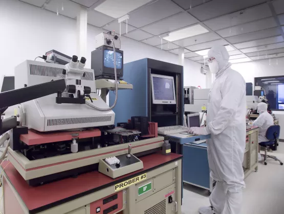
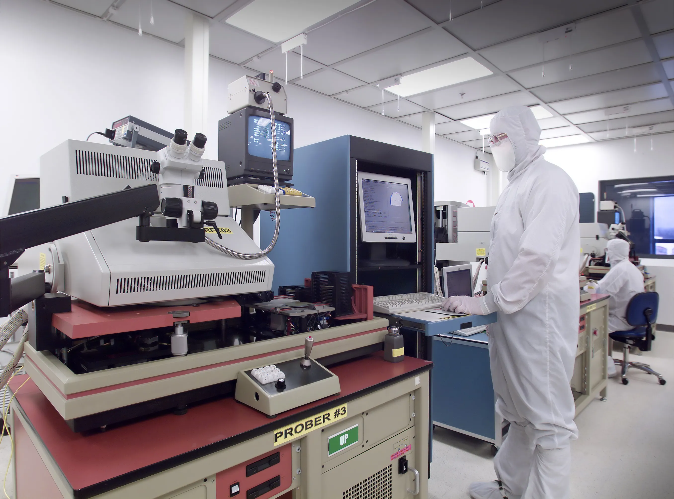
IntroductionStarting July 4, 2022, PFOA (Perfluorooctanoic acid) levels in semiconductor manufacturing and related equipment (SMRE), including replacement parts, entering the European Union (EU) will be restricted to 25 ppb per component (or any part thereof). Semiconductor equipment components (and the parts thereof) of particular concern include fluid tubing and fittings, pipe/seal tape, wire and cable insulation, filters, valves, tanks, panels, reaction vessels and o-rings; if they are made from fluoropolymers or fluoroelastomers.When PFOA is used as an aid to the manufacture fluoropolymers such as PTFE, PFA, PVDF or fluoroelastomers such as FKM and FFKM (collectively referred to as fluoromaterials), an unintended PFOA residue can be trapped within the fluoromaterial. Buyers of components used in SMRE are usually unaware of the processing method used for any fluoromaterials they may contain, and, as a consequence, the potential for PFOA residue. This lack of information about potential PFOA residues could result in regulatory enforcement actions and restricted market access, particularly in the EU.The impact of restrictions on fluoromaterials used in SMRE has been introduced in previous SEMI articles ‘Fluorinated Compound Restrictions May Trigger Costly Equipment Changes’ and ‘Fluorinated Substance Restrictions Triggers Costly Equipment Changes.’PFOA and its related compounds, such as the ammonium salt APFO (collectively called PFOA in this article), are recognized internationally as hazardous chemicals and are now targeted for regulatory restriction in the U.S., Taiwan, Canada and the EU. The UN Stockholm Convention on Persistent Organic Pollutants (POPs) is also considering listing PFOA, which could lead to additional international restrictions.The SEMI EHS Division PFOA Compliance Working Group has been working to understand: The likelihood of PFOA residue entering the supply chain of new components The residual level of PFOA in fluoromaterials produced prior to the phase out of PFOA by some manufacturers The impact of PFOA residue on the secondary equipment market This SEMI resource page, ‘Elimination of PFOA from the Equipment Supply Chain,’ and the supporting FAQ contain the Working Group’s key findings and conclusions.PFOA in the Fluoromaterial Supply ChainSignatories to the U.S. EPA Stewardship Program, which include FluoroCouncil members, eliminated PFOA from their manufacturing processes by 2013. However, other fluoromaterial manufactures – particularly in China, Russia and India – might still use PFOA and pose a significant risk to the worldwide supply chain.China, the world’s largest fluoromaterial producer, accounts for 53 percent of global production of PTFE and 38 percent of worldwide production of PVDF, FEP and FKM. An estimated 75 percent to 85 percent of fluoromaterials are manufactured using PFOA in China. Fully 25 percent of these fluoromaterials are exported, primarily to the U.S, Japan, EU and India. What’s more, finished goods made from or containing fluoromaterials that might be used as components in SMRE are exported from China.Documentation that traces fluoromaterials through the supply chain back to the original fluoromaterial manufacturer is key to meeting the PFOA regulatory requirements. This traceability can be straightforward in cases when an SMRE manufacturer directly specifies the use of a fluoromaterial in a custom-fabricated fluoromaterial component. However, for off-the-shelf components (e.g., cable ties, wiring insulation, tubing) or the components assembled from these components (e.g., controllers), the complexity and dynamics of the supply chain makes traceability back to the original fluoromaterial producer almost impossible.Residual PFOA Levels If, or how much, PFOA/APFO residue is contained in a fluoromaterial depends on the manufacturing process. Details of the manufacturing processes are proprietary and vary widely. Post manufacturing thermal treatments, such as sintering, extrusion, and molding, can result in the rapid thermal decomposition of APFO above 250C, but PFOA is significantly more stable. The temperature and time of thermal treatments is also proprietary and varies depending on the type of fluoromaterial and what is being made.This variability makes it impossible to estimate the likely level of trapped PFOA or APFO in a finished component or a part thereof. It is unwise to use data on the level of residue made known for one case to extrapolate the level of residue across the fluoromaterial industry. However, an industry-wide range on the order of 1ppm-10ppm (nearly 1000 times the EU limit) is suspected. Testing for the presence of PFOA/APFO at 25ppb in components is also problematic as there is no standard test method, and results among the custom methods developed in each test lab may vary.Given this uncertainty in test methods, a system of supplier declarations warrants consideration.Impact on Secondary (Used) EquipmentThe EU REACH restrictions apply to SMRE and replacement parts placed on the market at any time (not just initial placement – known as “first placing on the market”). For fluoromaterial components manufactured prior to 2013, there is a higher likelihood of residual PFOA/APFO levels exceeding the 25ppb limit of EU REACH. In principle all the SMRE components containing fluoromaterials should be investigated, and those containing PFOA above 25ppb must be replaced before the SMRE can be legally placed again on the EU market. Companies (e.g., semiconductor manufacturers) in the EU who wish to sell used equipment within the EU will be required to demonstrate the used equipment is in compliance. Selling older used equipment would likely be unprofitable after necessary investigations and component replacements are completed.Next StepsWhile the EU semiconductor manufacturing industry heavily depends on the secondary (used) equipment market, EU regulators may be unaware of the PFOA restriction’s damaging impact to this market. The EHS Division PFOA Working Group, in conjunction with SEMI Europe, is now considering how to bring this concern to the attention of regulators and to collaborate and lobby for effective changes including possible modifications to the EU Persistent Organic Pollutants (POPs) regulation.
Read More