downloadGroupGroupnoun_press release_995423_000000 copyGroupnoun_Feed_96767_000000Group 19noun_pictures_1817522_000000Member company iconResource item iconStore item iconGroup 19Group 19noun_Photo_2085192_000000 Copynoun_presentation_2096081_000000Group 19Group Copy 7noun_webinar_692730_000000Path
Skip to main content
Default Banner Image

fab

Back in 2012, China ranked fifth among seven regions worldwide in IC wafer capacity but surged past the Americas and Japan in 2018 and 2019 to claim the number three position (figure 1). That’s a big deal given that ICs account for the largest share of wafer capacity excluding discrete, opto, MEMS and sensors.China’s IC wafer capacity growth accelerated to tune of 14% in 2019 and 21% in 2020 and is expected to grow at least 17% this year, as we report in the latest update of the World Fab Forecast, published December 3rd by SEMI. Of all regions, Taiwan boasts the second strongest growth rate over the same period at 3% to 4%.Figure 1: Total IC installed wafer capacity for top five regions The report shows that from 2019 through the end of 2021 China will have increased wafer capacity for memory by 95%, foundry by 47% and analog by 29%. Foundry will represent the largest portion of those gains, reaching 2 million wpm (200mm equivalents). Memory will follow at about 1.5 million wpm and then analog at over 120,000 wpm.But Chinese companies aren’t pulling off this feat singlehandedly. Many international companies are contributing to the wafer capacity increases in China (figure 2). Figure 2: IC wafer capacity in China by company origin The share of capacity contributed by Chinese-owned companies and international companies has changed little since 2012, though Chinese-owned companies saw a slight dip in their slice of the pie from 60% to 57%From 2019 through 2021, Chinese-owned companies will add almost 60% capacity for foundries, the most of all sectors. Companies including SMIC, Hua Hong Semiconductor, Nexchip, XMC and Hua Li Microelectronics are driving the increases.During the same period, Chinese-owned companies will ramp up memory capacity from basically zero to 300,000 wpm. Companies such as Yangtze Memory Technology and ChangXin Memory Technologies (CXMT), also known as Innotron, are powering the quick rise with aggressive ramps of 3D NAND and DRAM capacity.Among international-owned companies, TSMC and UMC are driving the largest share of foundry growth, while Samsung, SK Hynix and Intel are powering gains in memory capacity.More information is available in the World Fab Forecast report. The report currently collects information for fab equipment and construction investment, capacities, technologies and product types for over 280 fabs and lines in China alone, including 40 facilities that either began operation in 2020 or will from 2021 through 2024.Christian G. Dieseldorff is senior principal analyst in the Industry Research and Analysis group at SEMI in Milpitas, California.
Read More
As a top semiconductor manufacturing hub, Korea is poised to lead the world in fab construction spending in 2019 and 2020, accounting for 27 percent of the total market. Little wonder that Korea’s prowess in the semiconductor industry has meant steady membership growth for SEMI Korea, with HD Cho, president of SEMI Korea, putting the average annual jump at about 7 percent.But HD Cho’s focus as he returned to COEX in Seoul, home to SEMICON Korea, in late August was not on membership growth over the years but the future. Cho hosted about 400 SEMI members gathered at SEMI Korea Members Day for insights into the state of the world economy, semiconductor industry outlooks, and perspectives on how South Korean and European microelectronics companies can form stronger ties. Setting the stage with look at macroeconomics, Byung-yeon Kim, team manager of NH Investment and Securities, predicted that, as the global economy continues to falter, 25 of the 58 major countries this year will cut interest rates in a bid to boost prospects for growth. Historically, the global composite leading indicator (CLI), a bellwether for turning points in the economy, has rebounded after 20 months of decline, he said. While the CLI downtrend is now past the 20-month mark, Kim struck a bullish note, predicting that the global economy will bounce back before long.Soo-kyoum Kim, vice president at IDC, referring to the semiconductor industry’s own soft patch, said that total revenue is expected to drop from $475 billion in 2018 to $440 billion this year but should rebound to a new high of $500 billion in 2023. The memory market will be especially hard-hit, dropping more than 29 percent in 2019 and another 14 percent next year before bottoming and then staging a recovery in the second half of 2020. The strength of the rebound will hinge on server market demand, he added.Next year will also see rebounds in semiconductor equipment and materials revenue, with growth of 12 percent and 3 percent, respectively, said Clark Tseng, director of Industry Research and Statistics at SEMI. The increases will follow a 2019 equipment market drop of 18 percent to $53 billion from the previous year while materials this year is expected to remain flat at $52 billion. The semiconductor industry will expand at a modest 2.4 percent this year, jumping to 7.6 percent in 2020, Tseng reported, citing the average growth rate based on data from Gartner, WSTC, IC Insights, VLSI Research and other industry analyst firms. Despite current weak market demand and the ongoing trade war, the long-term outlook for the semiconductor industry remains upbeat, he added.In Europe, semiconductor industry growth continues on the strength of the region’s high strategic importance in the global electronics supply chain, said Laith Altimime, president of SEMI Europe. Fab construction spending in Europe continued to grow in 2018, reaching $300 million, and is expected to hit $1.2 billion in 2019 and $1.6 billion in 2020, with equipment, parts and components driving the surges.To help build stronger ties between European and Korean chip industries, Altimime introduced the SEMI Korea members to SEMI Europe business platforms including SEMICON Europe, the 3D System Summit, ISS Europe, and the MEMS Imaging Sensor Summit. He also encouraged the formation of more business partnerships between companies in the two regions by familiarizing SEMI Korea members with European players in areas such as foundry, MEMS, sensors and wafer manufacturing.And it will be MEMS and sensors that help drive the 4th Industrial Revolution, said Sung-hyuk Kim, a team leader at LG Electronics' Sensor Solution Research Institute. In his presentation Architecting Sensor Solutions for the Next Revolution, he noted that sensors are finding their way into devices where they have never been used before. In household refrigerators, gas sensors help deodorize the inside while distance sensors detect the approach of people. Air conditioners equipped with a camera sensor can pinpoint the location of humans and steer the airflow in their direction. Of course, all these smarts will come in form of data-devouring artificial intelligence (AI), and that data will be generated in massive amounts by MEMS and sensors – placing them at the epicenter of the 4th Industrial Revolution.Jaegwan Shim is a marketing specialist at SEMI Korea.
Read More
This article is the fifth and final in a series highlighting the vital importance of SEMI Standards to commemorate the publication of the 1000th SEMI Standard in July 2019. Find the entire series here.As we define industry standards for managing data in the fab and beyond, we are creating a virtuous circle. More data create better processes. Better processes generate more good data, and more good data lead to better processes. It becomes a cycle of continuous improvement, and we are only just beginning to realize its potential. To dive deeper we interviewed Alan Weber, vice president, New Product Innovations at Cimetrix, and an active member of SEMI Standards Information and Control Committee (IC C).“Industry standards are critical in allowing us to collect information across the fab and use it in increasingly sophisticated control algorithms for the equipment,” said Weber. “The last few years have been about analysis applications that leverage big data in the fab. What started at the lot level is now applied at the wafer level, and for a process like lithography, it’s down to the shot or die level. We’re now collecting enough data variables at individual process and recipe steps to model for predictive maintenance and virtual metrology.”The migration from using data as rearview mirror for identifying and addressing fab issues to using data to head off issues preemptively represents a paradigm shift with immense advantages. This is the starting point for realizing a virtuous data circle.The benefits of a virtuous data circle are simple and compelling: higher yields, faster time to market, more revenue and greater profitability. Our optimism, however, is tempered by major obstacles to this promising future.Multilingual ManufacturingWeber points out that the electronics industry is becoming a multilingual standards world with more than 1,000 fab equipment vendors and several layers of protocols that present the challenge of seamlessly handling multiple protocols. His IC C Committee is out to tackle this challenge.“While SEMI Standards efforts first began in the front end, our standards program now encompasses the back end with test and packaging as well as other device areas including MEMS, sensors and displays,” said James Amano, senior director, International Standards and EHS, SEMI. “We’re going to see data connectivity from the front end to the back end to the final assembly of multi-chip products and that needs standards,” Weber explained. “We’ll need more connected equipment throughout the global, multi-site manufacturing process if we are to support the full traceability requirements of the most demanding markets such as automotive.”The industry will benefit from greater collaboration. Weber predicts that companies will team to create integrated supply chains within broader industry supply chains.Getting the Right People at the Right Time“As we lead the development cycle of a standard from concept to realization, one of the most important jobs of our standards task forces and committees is to coordinate competing companies and build an industry consensus,” Amano said. “This is the case for data in particular, where we rely on industry professionals like Weber and his colleagues, who are working to bring people together to collaborate on developing standards for connectivity and data sharing. It is that critical human element that allows SEMI to sustain our commitment to introducing standards that move the industry forward.”Will Companies Share Data If It Is Secure? Weber contends that when it comes to securing and sharing the data, the biggest challenge is to change the industry’s information-sharing culture.“Finance and defense are already finding ways to deal with data security,” said Weber. “While we will always have problems that require technology fixes, like dealing with new types of computer viruses, I am confident that we will be able to create standards that enable the free, secure flow of information. The key to making progress and better leveraging data is to get companies to see the potential of sharing data while investing in the standards.”SEMI recently launched a project to optimize data sharing across two critical process steps – lithography and plasma etch – to accelerate the adoption of data-driven AI methodologies. The results will help to establish data transfer and management standards crucial to the trusted exchange of trade secrets, IP and other sensitive information. Tools and materials from several SEMI members will be used for the project at Cornell University’s NanoScale Science Technology Facility (CNF). SEMI members are invited to join the project review team. Contact Pushkar Apte at SEMI ([email protected]) for more information on the initiative.Advantages Are Too Great to IgnoreTraditional cultural obstacles aside, the advantages of creating virtuous data circles are simply too great to ignore. Now that it’s accepted wisdom for fabs, factories and supply chains to continuously leverage interconnected data to get smarter, the time has come to extend those advantages throughout the full manufacturing process. Without these data circles, we’ll slow the development of new technologies and applications.We can only speculate where the lines of sharing data are drawn and will be redrawn in the future. But, without doubt, technology innovations such as AI will spawn new information business models that vertically and horizontally integrate companies in ways previously unimaginable. Data standards will underpin this structural transformation.Use your voice to affect standardization in and around the microelectronics industry. Learn about SEMI International Standards – and become part of the solution. Heidi Hoffman is senior director of technology communities marketing at SEMI. Hoffman and her team shine a spotlight on the work of the more than 20 technology communities under the SEMI electronics manufacturing supply chain collaboration platform. Actively engaging community members in marketing programs that showcase their unique value, Hoffman’s team helps companies to grow and prosper through the power of connection, collaboration and innovation.
Read More
This article is the fourth in a series highlighting the vital importance of SEMI Standards to commemorate the publication of the 1000th SEMI Standard in July 2019. Find the entire series here.Computer prices have plunged over the years even as desktop and laptop PC performance has skyrocketed thanks to the semiconductor industry, giving users much more bang for their buck. The chip industry stands in a stark contrast to healthcare and education with their exponentially rising costs.What distinguishes the semiconductor industry from healthcare and education in the capacity to deliver so much for so much less over time? After all, even in other parts of the technology sector that are heavily regulated, such as cable television, we have not witnessed the same price decreases as in microelectronics.Some pundits claim that the difference among sectors is tied to their degree of regulation. Does greater regulation somehow degrade product value? The reality is far more nuanced. But one thing is clear: Smart self-regulation (i.e. standards) in the semiconductor industry has contributed mightily to its success.The recipe for success has been simple. Standards have been rocket fuel for competition, which in turn has sparked innovation, driving down device prices while boosting performance. Computer prices fell dramatically between 1997-2015 while the cost of cable TV and internet services rose. Myth of unregulated competitionA semiconductor fab might actually be the most regulated place on earth. Fabs hew to a much higher standard of air quality and cleanliness than even uber-sterile hospital operating rooms. Manufacturing processes are voluntarily regulated not to millimeters, but to nanometers. While some standards are proprietary with limited reach, others span the supply chain. Regulation has worked so well in this sector that the semiconductor industry isn’t moving toward less standardization. It’s moving toward more. Secret is smart standards The gap between regulation and self-regulation is more like a chasm. We typically view regulation as a series of top-down directives that more often focus on the interests of the producer than the consumer. Healthcare regulation, for example, may improve quality of care, but it’s often insurers, big pharma and hospitals that benefit most from regulation, rather than consumers.The semiconductor industry, on the other hand, uses self-regulation to improve business operations and make better products for consumers. Falling prices and rising performance are natural byproducts.Semiconductor industry self-regulation is an ecosystem-wide effort, where input isn’t just top-down, but also bottom-up or even side-to-side. The first SEMI Standard, which specified wafer sizes, exemplifies this approach.The SEMI Standards Committee formed in 1973 to address silicon wafer dimensional specifications. At the time, wafer specifications proliferated. Numbering more than 2,000, the various specifications led to major inefficiencies just when the industry was just getting underway. Wafer suppliers banded together under SEMI to solve this problem and rapidly developed consensus specifications for 2- and 3-inch wafers. By the mid-1970s, over 80% of wafers conformed to these new standards.Standardized wafer sizes freed equipment companies to focus on innovations that reduced cost and increased performance. It also allowed manufacturers to focus on product differentiation without having to worry about device fabrication process and cost. Since that first SEMI Standard made possible the modern semiconductor equipment industry, original equipment manufacturers (OEMs) have competed to deliver amazing innovations. For example, lithography systems routinely use light to design chips with feature sizes smaller than the wavelength of light.SEMI’s 1000th standard on energetic materials demonstrates how smart standards are also pragmatic. This standard is not about banning materials or assigning blame when things go awry. It is about creating practical guidelines that companies will follow, enabling them to realize greater innovation. Guidelines that reduce accidents and risks will spur more, not less, energetic materials’ exploration. Industry suppliers will be the big winners.The 1st to the 1000th SEMI standard all represent examples of cooperation making more sense than competition.Standards for the real worldCreating a business-friendly standard that still gets the job done is a process. As SEMI Standards Task Force and Committee members, materials, equipment and manufacturing companies take part in defining best practice guidelines that support safe and practical use of materials and equipment. Task force and committee members assign particular responsibilities and associated costs to the most logical segments of the supply chain. They also develop information-sharing practices around competitive process recipes and purity standards.Andy McIntyre, CIH, a member of the energetic materials task force and an executive vice president and managing principal at BSI EHS Services and Solutions, summarized what makes SEMI standards smart.“SEMI standards are pragmatic,” said McIntyre. “They take into account the need for implementation in a real-world business environment. They embrace an engineering approach to problem-solving to create practical solutions, and they define specifications and performance goals in ways that allow engineers — in collaboration with EHS professionals — to identify practical solutions for reducing risk in R D, pilot line and manufacturing operations.“SEMI standards employ a holistic process that considers all the important points of view throughout the supply chain, from materials selection, installation, use, recycling and/or disposal,” said McIntyre. “The breadth of SEMI EHS Guidelines, for example, is also very comprehensive as the SEMI EHS Committee and task forces work to ensure that standards keep pace with dynamic technology developments. Energetic materials is a prime example where the industry recognized the need for a new safety guideline to document safe usage of pyrophoric, water-reactive and unstable reactive materials, which have become increasingly important in semiconductor and advanced materials R D and manufacturing.”This is the real secret to the success of the semiconductor industry. Smart self-regulation allows industry players to cooperate in the development and implementation of standards that are pragmatic, comprehensive and dynamic. Participants in SEMI Standards have a voice in the semiconductor industry because they are the voice of the semiconductor industry.While innovation in semiconductors may not always keep pace with Moore’s Law, we can depend on one truth: As long as collaboration and cooperation are the rule and not the exception, we will continue to advance technology in amazing and unprecedented ways. You, me and all other consumers will continue to reap the rewards of innovation. Use your voice to affect standardization in and around the semiconductor industry. Learn about SEMI Standards – and become part of the solution.Heidi Hoffman is senior director of technology communities marketing at SEMI. Hoffman and her team shine a spotlight on the work of the more than 20 technology communities under the SEMI electronics manufacturing supply chain collaboration platform. Actively engaging community members in marketing programs that showcase their unique value, Hoffman’s team helps companies to grow and prosper through the power of connection, collaboration and innovation.
Read More
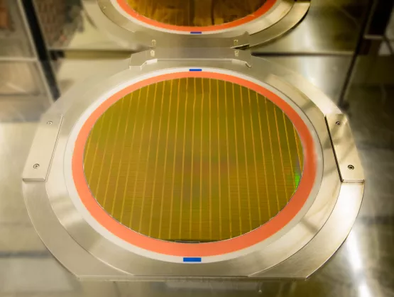
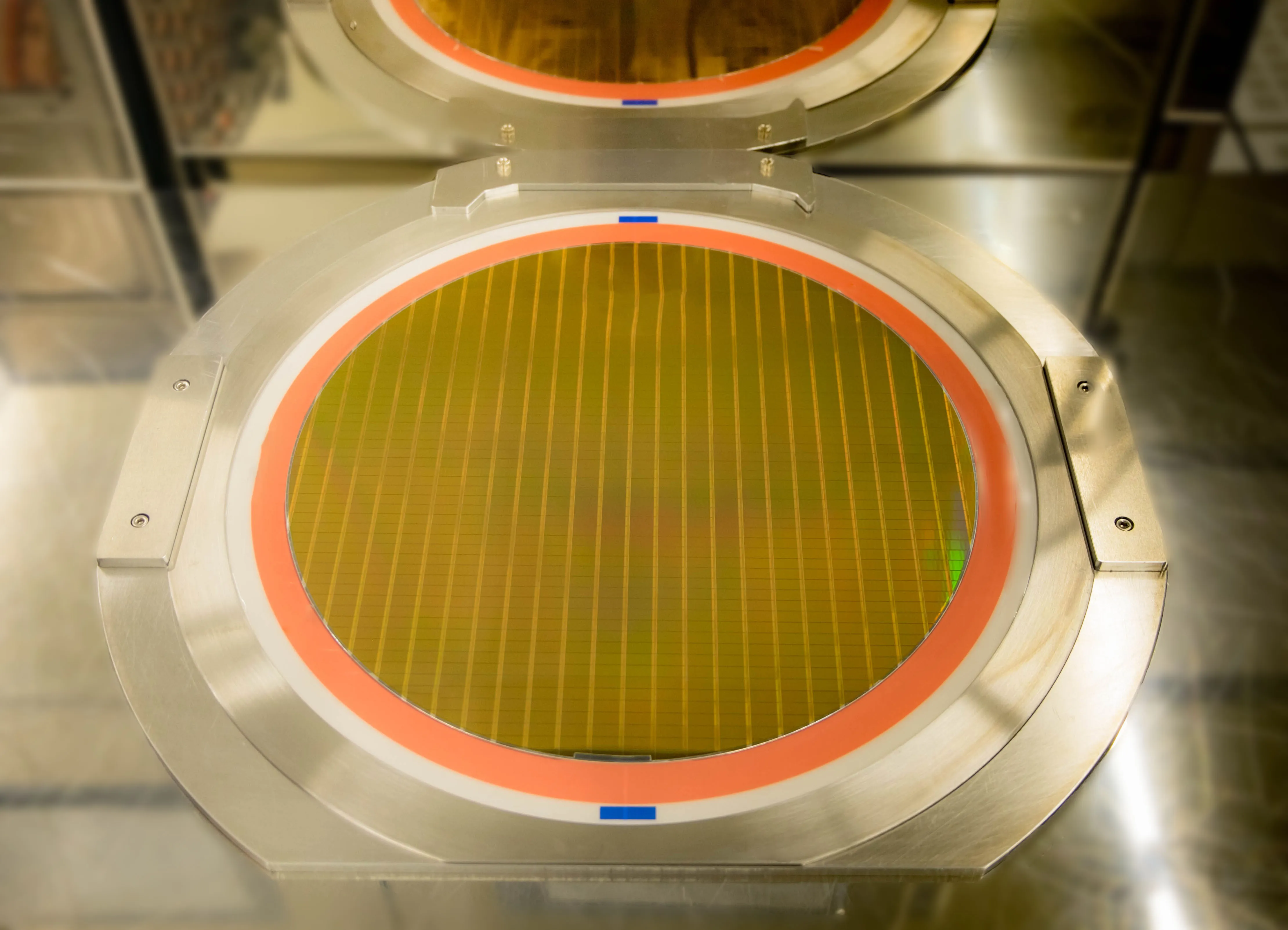
This article is the third in a series highlighting the vital importance of SEMI Standards to commemorate the publication of the 1000th SEMI Standard in July 2019. Find the entire series here.SEMI Standards are the bedrock of the modern microelectronics industry. Without standards for wafer dimensions – which SEMI Standards first defined through a collaborative process involving semiconductor manufacturers and wafer suppliers in 1972 – the semiconductor equipment industry as we know it would not exist today. The late Robert Noyce of Intel noted in this 1992 video “being good at producing semiconductors will mean we have better, more consistent, better controlled equipment than we have in the past. Standards are going to play a vital role in that. Standards saves money and time for everyone.” Noyce also called standards a bellwether to surges of innovation in critical process technology. This is still true today as, for example, important standards-setting activity is afoot in panel-level packaging, electron microscopy and energetic materials. Will a surge of innovation follow?Panel-level packaging: a chicken-egg scenarioFrom advanced materials to more efficient production tools, one hallmark of the microelectronics industry is our fearless exploration of new technologies that will spawn change across the industry by improving performance and reducing cost. Advanced packaging techniques, such as panel-level packaging (PLP) – which moves semiconductor packaging to a larger-panel format – is one of those critical catalysts. Citing PLP’s potential to shrink costs by improving efficiency and economies of scale, research firm Yole Développement predicts a remarkable 63% CAGR for PLP from 2017-2023.[i]It’s no stretch to say that we are close to realizing a burst of innovation in packaging. With a just-published SEMI Standard (SEMI 3D20) specifying panel sizes, equipment companies will find it economically viable to invest more in developing the much-needed production tools that enable PLP. “It is really important to create standards so we come together and work much more efficiently. Creating those fundamentals allows you to be more productive in the long term,” said Christina Chu, ASM Semiconductors, and co-leader of the Panel Level Packaging Task Force, and one of five industry leaders recognized for their outstanding accomplishments in developing SEMI Standards for the electronics and related industries at the recent 1000 SEMI Standards reception during SEMICON West 2019. “This effort came up from the trenches,” said Richard Allen, NIST Quantum Measurement Division, and a co-leader of both SEMI’s 3D Packaging and Integration Committee and its Panel Level Packaging Task Force. “Equipment vendors told us that they wanted to serve the market, but they couldn’t do so without some standards. To respond to their request, our committee surveyed the market and discovered at least 15 different panel sizes in development.”“As no vendor is going to make over a dozen unique tools for the same process, we worked with the manufacturers and tool companies to write a specification that standardizes on two of the most widely accepted sizes,” Allen said. “For the first time, the industry will have a real market for panel-level packaging tools, and that will spur commercialization of new technologies that never would have seen the light of the day without standardization.”Allen pointed out that evolution of standards in microelectronics reflects the dynamism of the microelectronics industry itself. “Given the rate of technology advancement in microelectronics, SEMI Standards committee and task force members know that a newly-published standard is often just a starting point, and change will likely follow,” he said. “The Panel Level Packaging Task Force, for example, is currently determining how to best support this packaging technology, whether through possible enhancements to 3D20 or by creating new PLP standards.”Process automation is key for TEMTransmission electron microscopy (TEM) is another area where industry cooperation will fuel progress.“People throw around the phrase ‘exponential growth,’” said James Amano, senior director, International Standards at SEMI. “It’s usually a gross exaggeration, but not when it comes to TEM data. That’s because demand for more TEM data, which uniquely enables innovations around smaller feature sizes, has exploded. At the same time, TEM data is a bottleneck in the fab. Operators literally use tweezers to carry around electron microscope samples by hand, and that is untenable.” TEM sampling standards are currently being formulated under the SEMI Standards development process. “Applying a model that we have employed successfully time and time again through SEMI Standards, we are gearing up for process automation in TEM,” Amano said. “We’ll start by establishing a grid carrier standard for electron microscopy. Through ongoing standards efforts, we may realize a fully automated TEM process within just a few years. That achievement will enable exponential growth in shrinking design geometries.”Energetic materials gain safety standardAlong with wafer-level packaging and design shrinks, the push for safety in materials’ usage is a hotbed of innovation. This is especially true with energetic materials, the potentially hazardous process chemicals used increasingly in semiconductor manufacturing to spur advances in materials purity, integrity and quality.“When you’re working with energetic materials, if you don’t get it right, you may face serious yield and cost issues, and most important of all, safety risks,” said Paul Trio, senior manager of strategic initiatives at SEMI. “This isn’t a theoretical concern. Real problems occurring in fabs have made an energetic-materials standard a high priority for the industry.”“After years of collaborating with companies across the supply chain to address this significant challenge, we recently published our 1000th SEMI Standard around safe usage of energetic materials,” Trio said. “Now manufacturers can turn to a new standard – which will evolve dynamically in response to industry changes – as they employ energetic materials in their quest to achieve higher yields while controlling costs and managing safety risks.” Whether it’s packaging, design shrinks, materials or other key innovations, standards are essential to progress in microelectronics. From equipment and materials suppliers that provide the most advanced, efficient and safest tools, materials, and processes to device manufacturers that get products to market, all stakeholders in the microelectronics ecosystem benefit from SEMI Standards. Are you curious about the areas of process technology where innovations are likely to occur? Would you like to get involved in standards efforts that could have an impact on your business? Take a look at the activity of SEMI Standards Committees and Task Forces. Because that’s where innovation, pragmatism and a commitment to harness industry resources come together.Use your voice to affect standardization in and around the microelectronics industry. Learn about SEMI Standards – and become part of the solution. Heidi Hoffman is senior director of technology communities marketing at SEMI. Hoffman and her team shine a spotlight on the work of the more than 20 technology communities under the SEMI electronics manufacturing supply chain collaboration platform. Actively engaging community members in marketing programs that showcase their unique value, Hoffman’s team helps companies to grow and prosper through the power of connection, collaboration and innovation. [i] Status of Panel Level Packaging report, Yole Développement, 2018
Read More
This article is the first in a series highlighting the vital importance of SEMI Standards to commemorate the publication of the 1000th SEMI Standard in July 2019. Find the entire series here. More than 40 years after establishing the SEMI International Standards program, SEMI recently announced its 1000th SEMI Standard – a safety guideline for handling energetic materials. Creating a resource for unpredictable changes in materials is the type of challenge the SEMI International Standards program is often called upon to tackle – where the standard is merely the end of the beginning. The semiconductor industry has learned to expertly control its facilities, equipment and components. The next logical step is materials. It’s common knowledge that the industry drives innovation with new process materials and enabling safer material exploration is critical to the industry’s success. Classification Schema The 1000th SEMI Standard provides three classifications of energetic materials and byproducts based on three criteria: Hazardously exothermic (large amount of heat released following a trigger event such as heating or a physical shock) Pyrophoric (self-igniting upon air exposure) Water-reactive (releasing a large amount of energy or flammable gas upon contact with water) Unsafe handling of any of these byproducts can, to put it mildly, result in a bad day for a fab or lab. The leader of the Energetic Materials Task Force and an expert in process and equipment risk assessment at his company Safety Guru, Eric Sklar recounted one of the stranger incidents. A cleaning crew detached a pipe from a piece of equipment associated with a process recipe that used no energetic materials. The team set it in a sink, sprayed some water to begin cleaning it, and the pipe ignited in flames. Remarkably, although the initial materials weren’t energetic, the process created new byproducts that were very much so. Standardizing on Shifting Ground Energetic materials are new ground for standards and that ground is shifting, with much more material innovation to come. The upshot is that it is particularly important that the energetic materials standard is dynamic. By design, all SEMI Standards are malleable – continuously shaped by the demands they aim to meet. The release of this document is nowhere near the end of the work, as the standard will evolve to keep pace with continuing materials innovation. Creating a Robust Materials Supply Chain SEMI Standards create the conditions for a more robust materials supply chain and sustain the needs of business. If the standards safeguards are too burdensome, they will never be adopted. Conversely, without protections, people and equipment are unnecessarily put in harm’s way and innovation slows. SEMI’s Energetic Materials Task Force members realized early on that the industry needed a standard that would be practical to implement and flexible enough to be optimized over time. They understood that collaboration and compromise, while time-consuming, are also essential for standards’ creation. They determined roles and responsibilities across the supply chain, and they struck delicate balances between sharing no information about the intended uses of potentially dangerous materials and sharing everything about proprietary process recipes. The sheer scope of this standard necessitated a multi-year timeline. “The effort began with SEMATECH assembling its members’ views about energetic materials safety,” said Eric Sklar. “It then required years of effort from SEMI to bring the key industry participants together to create pragmatic guidelines that address the challenges around energetic materials in the supply chain.” Only Getting Started Despite all the work, one certainty is that the standard isn’t perfect for the present and can’t reflect future demands. This is why the energetic materials standard is not a static document, but a living process that is in its germinal stages. Key players continue to shape the standard, and that’s fundamental to enabling future materials innovation and ultimately reducing the number of unexpected energetic materials reactions in fabs. The variables in standards development are numerous and ever-changing. Energetic materials only magnifies the need for the broad collaboration that SEMI has facilitated for more than 40 years. While the risks posed by energetic materials are substantial, the criticality for continued innovation is undisputed. Now, with its adoption, the work of adapting and modifying this 1000th SEMI Standard is only about to begin. Use your voice to help drive standardization in and around the semiconductor industry. Learn about SEMI Standards – and become part of the solution. Register to receive Standards Watch, SEMI’s quarterly e-newsletter. Heidi Hoffman is senior director of technology communities marketing at SEMI. Hoffman and her team shine a spotlight on the work of the more than 20 technology communities under the SEMI electronics manufacturing supply chain collaboration platform. Actively engaging community members in marketing programs that showcase their unique value, Hoffman’s team helps companies grow and prosper through the power of connection, collaboration and innovation.
Read More
This year, SEMI ISS covered it all – from a high-level semiconductor market and global geopolitical overview down to the neuro morphic and quantum level. Here are key takeaways from the Day 1 keynote and Economic Trends and Market Perspectives presentations.In the opening keynote, Anne Kelleher from Intel pointed to the huge growth of data, with fabs collecting more than 5 billion sensor data points each day. The challenge, Kelleher noted, is to turn massive amounts of data into valuable information. Moore’s law is not dead. New models of computing benefit still from Moore’s law and advances in Si/CMOS technologies for conventional, deep learning, neuro morphic and quantum computing.With customers expecting continual improvements in applications, the question is whether the chip industry is moving fast enough to meet these expectations, Kelleher said. A broad supply chain, equipment and materials innovations, and attracting the “best of the best” college graduates to fuel innovation is key, she said.In the economic trends session, Nicholas Burns (ambassador ret.) from Harvard University pointed out that we will see a major shift in power. The U.S. will remain the major world power over the next 10 years, but we will see a major shift in power in the next coming decades as the gap with countries like China, Russia and India continues to narrow.Duncan Meldrum from Hilltop Economics said that we are passing the peak growth of economic cycle. He warns that a more likely outlook is that a global growth recession is developing. Although semiconductor MSI growth will see a noticeable slowdown in 2019 and 2020, the semiconductor industry is still healthy over the longer term.Bob Johnson from Gartner sees demand shifting from consumer to commercial applications with higher ROIs and budgets. AI, IoT and 5D are the major enablers. He sees structural changes in the semiconductor industry especially for memory but also for Moore’s law with increasing costs and fewer players.The DRAM markets shows volatility and NAND market may be negative in 2019 but non-memory are expected to accelerate mainly because of increasing content and some price hikes.Overall Gartner expects good long-term growth with a CAGR (2017 to 2022) of 5.1%, outpacing 2011 to 2016 CAGR of 2.6%. After a strong 2018 with 13.4% revenue, he forecasts a slower 2019 with 2.6% growth followed by a 8% growth in 2020 and negative growth rate in 2021.Andrea Lati of VLSI went “Back to fundamentals” in his presentation about the industry. VLSI sees a downside bias due to slowing global economy, tariffs, and trade wars. Future drivers are data economy, cloud, AI and automotive.As memory leads the 2019 slowdown, analog, power, logic and other sectors remain in positive territory. VLSI lowered its semiconductor equipment forecast for 2018 from 20% (Jan. 2018) to 14% (Dec. 2018) but increased its sales outlook from 8% to 15% in 2018. VLSI expects revenue to slow into the first half of 2019 but increase to over 4% in the second half of the year, resulting in total 2019 drop of 2.7%. Semiconductor equipment sales are expected to drop from 14% in 2018 to -10% in 2019.Michael Corbett of Linz Consulting, covering wafer fab materials in the years of 3D scaling, sees these as good times for the industry. His outlook for wafer fab materials is bullish based on strong MSI and because wafer fab materials suppliers are getting bigger because of M As.In the Market Perspective session, Sujeet Chand of Rockwell Automation pointed out that as more and more data is generated, the problem is how to get value of all the data collected. There is a need to create the right architecture for machine learning and AI and big data is increasingly being replaced by contextual/structured data. He expects Industry 4.0 to drive foundries to become smaller, more flexible and more productive.In the Technology and Manufacturing session, Aki Sekiguchi of TEL addressed process challenges in the age of co-optimization. The semiconductor industry continues to expand, driven by massive growth of interconnected devices, with heavy demand for processing power and storage. He expects an exponential increase of data from about 40ZB in 2018 to 50ZB in 2020 to 163 ZB in 2026.Major technologies such as DRAM, 3D NAND and logic are dealing with scaling challenges. The density of DRAM (Mb/chip) is plateauing according to 2015 to 2020 trend data, with DRAM is in need of EUV. Memory capacity demand is leading to increasing layers and higher aspect ratios that is concern for 3D NAND and mainly for plasma etch. With Logic already implementing 3D structures, it appears to be in a solid position. Buddy Nicoson of Micron talked about his 50 years in the industry and looked ahead to the next 50. The anchors – quality, cost, scale and speed – won’t change. It has been a great journey so far with unprecedented opportunities and challenges ahead of us. We are getting into a convergence (specialization, integration) and solution-based phase. We will see some inflection points in the coming years, with the best yet to come.Christian G. Dieseldorff is senior principal analyst in the Industry Research and Analysis group at SEMI in Milpitas, California.
Read More
Micron, one of the top three memory semiconductor companies, reported solid results for the fourth quarter of fiscal 2018 (June to August) to extend a multi-quarter string of strong growth. However, the company’s mediocre guidance for the current quarter has raised concerns that memory demand will start to slow.To shed light on this super memory cycle, which began in the second half of 2016, this article examines correlations among the top three memory suppliers’ sales revenue, quarterly inventory levels, World Semiconductor Trade Statistics (WSTS) market data, and memory fab equipment investments reported by SEMI.The Memory Inventory Cycle Index, which is based on financial data reported by Samsung, SK Hynix and Micron, is the difference between the year-over-year growth rates of sales (or shipments) and inventories. The index explains business cycle fluctuations such as expansions and contractions, trending up in expansions and declining in contractions. Figure 1 shows both historical Micron sales (blue dotted line) and the quarterly Memory Inventory Cycle Index (black solid line). To minimize seasonal fluctuations, both were calculated based on a four-quarter moving average of sales and inventories. Figure 1. Memory Inventory Cycle Index Compared to Memory Sales* Remarks1) Memory Inventory Cycle Index = YoY growth rate of memory sales revenues - YoY growth rate of memory total inventoris value on a four quarters moving average.2) Calculated memory sales and inventoris are based on Samsung, SK Hynix, and Micron public announcements.3) South Korea Won were converted to US$ based on the quaterly average value released by FRED.4) Companies’ sales data were calculated based on 4-quarter moving average.5) Company data complied by SEMI. As shown in Figure 1, the Memory Inventory Cycle Index has been declining since peaking in the fourth quarter of 2017, mirroring the previous two contractions – in 2010 and 2014 – in which memory sales slowed or stagnated after four quarters of the index decline. Accordingly, if this relationship holds between the Memory Inventory Cycle Index and sales, Micron’s sales will slow in the coming quarters and is consistent with Micron’s guidance for the current quarter. Moreover, the index suggests that the sum of three companies’ sales (the solid red line) will exhibit a similar trend of decreased growth in the coming quarters, which will impact the annual growth rate of global memory sales.WSTS recently increased its 2018 forecast for memory sales to 30.5%, up from 26.5% projected in June of this year. However, the 3-month moving average of memory sales shows that memory sales already increased by 48% YoY in the first half of the year, which means growth is expected to be lower in the second half of the year. Other signs pointing to a weaker end to the year include front-end equipment investments by the top three memory suppliers. SEMI is modeling an annual increase of only one percent for the year for these suppliers, with spending down 23% in the second half relative to the first half of the year.Figure 2 shows the historical trend of the Memory Inventory Cycle Index, the YoY growth rate of memory sales, and YoY memory fab equipment investments. The Memory Inventory Cycle Index increased faster than memory sales and fab equipment investments in the past two cycles. In the most recent memory cycle, these three indexes are moving in tandem, each peaking in the fourth quarter of 2017. Figure 2. Memory Inventory Cycle Index, Memory Sales and Memory Fab Equipment Investments* Remarks1) Both sales and memory fab equipment investments data were calculated based on 4-quarter moving average to minimize seasonal fluctuation.2) All data are from SEMI, except memory sales (WSTS) While overall memory sales continue to be strong this year, memory ASPs have shown signs of weakening right after the inventory index peak. NAND flash ASPs have been trending downward since the first quarter of 2018. With the recent inventory correction and short-term CPU shortage, DRAM ASPs are expected to soften in the fourth quarter of 2018. The looming memory market slowdown has memory makers adjusting their capacity expansion plans for the rest of this year. Some new capacity additions, especially for DRAM, have been pushed out to 2019. The memory inventory cycle index has to some extent foretold the slowdown of the memory market. In the second and final part of this article, we will discuss the correlation between the Memory Inventory Cycle Index and China’s semiconductor sales and Purchasing Managers Index. We will also look at the increasing level of memory inventory in the past few quarters and its composition including Work-in-Progress and Finished goods. Clark Tseng is director and Sungho Yoon is senior market research analyst in Industry Research and Statistics at SEMI. SEMI World Fab ForecastFor the latest worldwide memory fabs forecast including company details, please see the SEMI World Fab Forecast. The report includes quarter-to-quarter fab data from planning to production for both DRAM and NAND Flash companies.
Read More
Tracking toward even stronger growth than forecast last year, 200mm fabs worldwide are gearing up to add more than 600,000 wafers per month from 2017 through 2022, an 11 percent growth rate that will lead to a new high of 6 million wafers per month by the end of 2022, according to the SEMI Industry Research and Statistics group in its fourth update of the Global 200mm Fab Outlook report. See chart below. All told, 56 older and newer facilities will add capacity, with the MEMS, power, logic and foundry segments contributing the most. To help meet rising demand, new fabs are under construction. Only six facilities plan to reduce capacity. The global 200mm fab count will increase from the 2017 level of the 194 fabs covered in the report to 203 by 2022. See chart. During the five-year forecast period, China, at 44 percent, is expected to account for the greatest growth, followed by Southeast Asia (19 percent), Taiwan (10 percent) and the Americas (8 percent). However, with strong demand for new 200mm fab equipment, the used 200mm fab equipment market has pretty much dried up. What’s more, the availability of key tools and spare parts has become a primary concern for many device makers. These headwinds notwithstanding, many companies remain bullish with plans to add more capacity. The forecast growth of 600,000 wafers per month may ultimately be a conservative estimate. SEMI’s Global 200mm Fab Outlook report lists more than 300 facilities and lines managed by more than 150 companies, providing details on product type, investment, technology and capacity plans by companies and fabs. The fourth update of the Global 200mm Fab Outlook report covers data and predictions from 2011 through the end of 2022, including milestones, detailed investments by quarter, product types, technology nodes and capacities down to fab and project level. Click here for the Global 200mm Fab Outlook Sample Report. Learn more about other SEMI fab databases at www.semi.org/en/MarketInfo/FabDatabase. Christian G. Dieseldorff is director of Industry Research and Statistics, SEMI, Milpitas, California.
Read More