downloadGroupGroupnoun_press release_995423_000000 copyGroupnoun_Feed_96767_000000Group 19noun_pictures_1817522_000000Member company iconResource item iconStore item iconGroup 19Group 19noun_Photo_2085192_000000 Copynoun_presentation_2096081_000000Group 19Group Copy 7noun_webinar_692730_000000Path
Skip to main content
Default Banner Image

SEMICON China

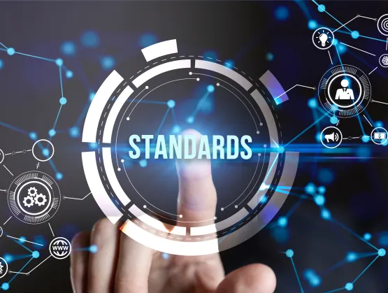
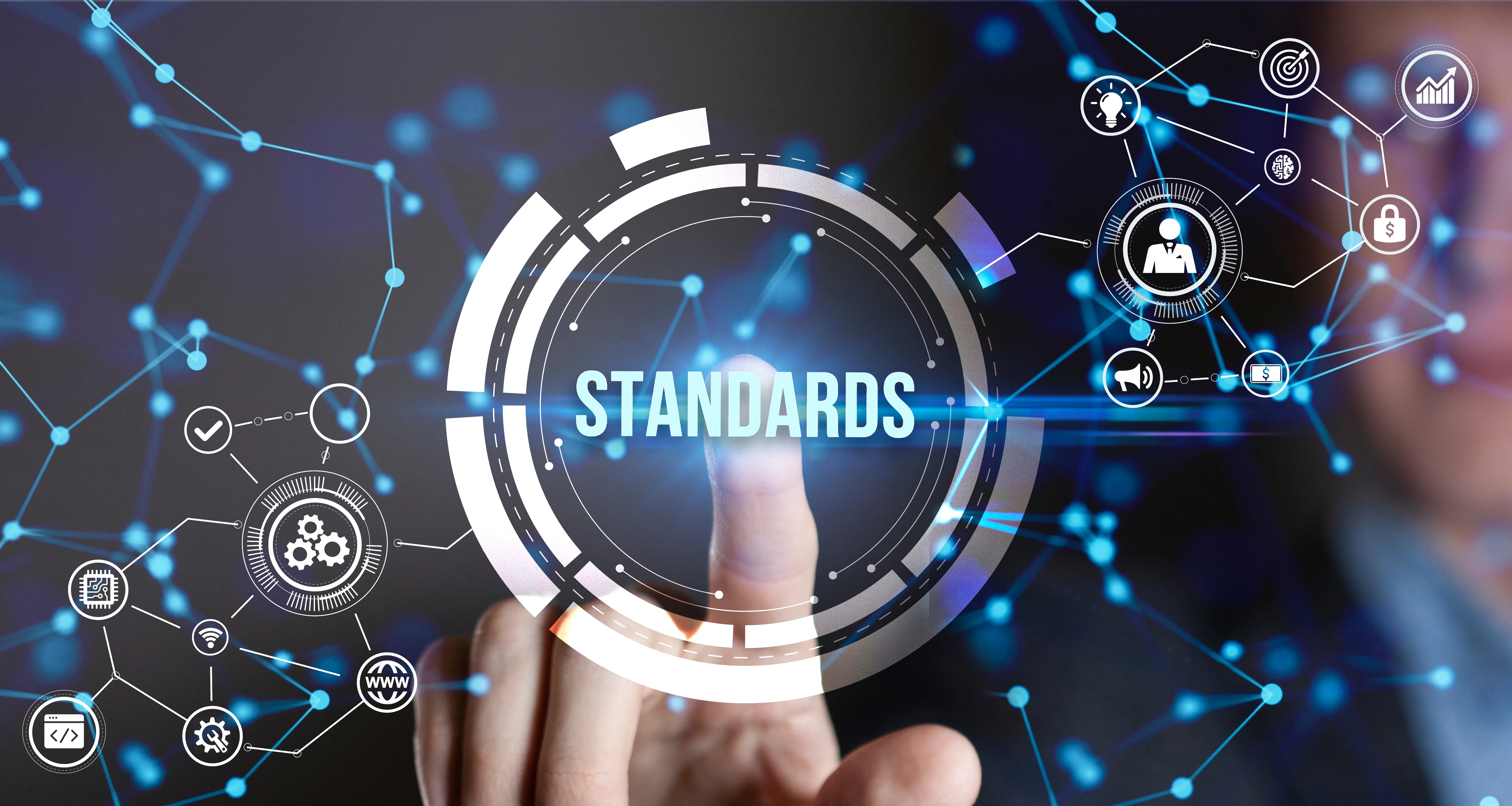
The SEMI Standards team hit the ground running in 2026, starting this year with an important milestone to our Flexible Hybrid Electronics (FHE) standardization efforts. As FHE technology continues to evolve into a scalable and manufacturable class of systems, we’re excited to share the upcoming release of SEMI 7242, Guide for Reliability of Flexible Hybrid Electronics. This is the first time a comprehensive framework for reliability assurance in FHE systems has been created, closing a critical gap within the industry landscape. Published as SEMI FH5, the standard is now available online via the SEMI Store or through a SEMIViews license.We’d also like to highlight a pending revision for SEMI E142, Specification for Substrate Mapping. While SEMI E142 is currently designed to work with other SEMI data exchange Standards, SEMI Draft Document 7381 proposes a subordinate standard to define maps to and from non-E142 wafer coordinate systems. Meanwhile, the Information Control Japan Technical Committee (TC) announced its new Maintenance Robot Communication (MRC) Task Force for standardizing communications for robotic maintenance systems to improve production efficiency and workloads in fabs. This quarter also included key developments from both SEMICON Korea and SEMICON China. At SEMICON Korea, members of the Semiconductor Manufacturing Cybersecurity Consortium (SMCC) discussed a unified, standards-based approach for strengthening cybersecurity amidst evolving digital threats. A month later, SEMICON China served as the backdrop for the EHS TC Chapter Formation Group Meeting, where attendees discussed critical safety, material usage, and energy efficiency standards. The North America (NA) Winter Meetings, held virtually in February 2026, also brought several TCs together to revise standards for MEMS, advanced packaging, EH S, Facilities, Gases Liquid Chemicals, factory automation, and more. For more than 50 years, the SEMI Standards International Program has worked to advance manufacturing processes, lower costs, and support key industry growth markets. To get involved in future developments, become a member of the SEMI Standards Program. Membership is free.With so much underway in Q1, we look forward to an incredible year ahead. Q1 2026 Highlights A New Standard for Flexible Hybrid Electronics As the first consensus-driven framework for reliability assurance in FHE systems, SEMI 7242, Guide for Reliability of Flexible Hybrid Electronics, was created to ease roadblocks for transitioning and commercializing FHEs. It aims to speed design cycles, improve comparability of test results, reduce the risk of integrating FHE into operations, and instill confidence for scaling FHEs from prototypes to high-volume production. Document 7242 was drafted by the FHE Reliability and Testing Task Force, with added participation from industry, academia, and government laboratories.The elevation of Document 7242 to a formal SEMI Standard reflects the field’s progression to a stage where consistent approaches to reliability are both feasible and necessary. As FHE adoption grows across medical, industrial, consumer, and defense applications, Document 7242 will support systems that offer dependable performance and sustained durability over time. Document 7242 also joins the recently published SEMI FH6 Standard on FHE Terminology.Revisions to SEMI E142SEMI E142, Specification for Substrate Mapping, defines data items required for reporting, storing, and transmitting map data for substrates. It was developed to work alongside other SEMI Standards to exchange data through a SECS/GEM interface. Identifying failure points requires a two-dimensional XY coordinate map generated for substrates. However, because some steps in the semiconductor manufacturing process may use their own XY coordinate systems, a revision is currently needed to define an infrastructure for mapping a non-E142 wafer XY coordinate system to and from the E142 Standard XY coordinate system.The Advanced Backend Factory Integration (ABFI) Task Force will ballot this potential subordinate standard from August 19 to September 18. It will be adjudicated during SEMICON West from October 13-15, 2026 in San Francisco, California.Introducing the Maintenance Robot Communication Task Force As the industry moves toward smart manufacturing, integrating robot-based maintenance solutions is becoming increasingly important for enhancing production efficiency, reducing workload, and ensuring consistent work quality in automated environments. The Maintenance Robot Communication TF was formed to address the critical need to standardize operational communications for robotic maintenance systems. A dedicated community page is now available on the Connect@SEMI platform for members to exchange ideas. This activity joins the recently established Mobile Maintenance Robot Safety Task Force which aims to develop new safety guidelines that are deemed necessary to fill the gaps between existing industry standards including SEMI Safety Guidelines with regard to safe operation of mobile maintenance robots.Standards Activities from Europe Spring MeetingThe Compound Semiconductor Materials Europe TC Chapter held its annual virtual Spring Meeting on April 14, 2026. The meeting drew robust participation from China, Japan, Europe, North America, and other regions. The TC Chapter successfully adjudicated document 7111, Revision of SEMI M81-0418, Guide for Defects Found in Monocrystalline Silicon Carbide Substrates. The major update provides significant guidance on defects in silicon carbide substrates. This document has been forwarded to SEMI Publications for final processing. The Europe TC Chapter will reconvene November 10–13, 2026, during SEMICON Europa in Munich, Germany.Underscoring the Need for Cybersecurity Standards at SEMICON Korea SEMICON Korea featured more than 200 speakers who shared insights and presented solutions that are shaping the modern AI era. From February 11-13 in Seoul, the conference also served as a meeting point for the next generation of SEMI Standards. Most notably, leaders from the Semiconductor Manufacturing Cybersecurity Consortium (SMCC) highlighted the strategies and operational frameworks needed to modernize cybersecurity protocols. SEMICON Korea Highlights:Applied Materials’ Suk Won Kang discussed SMCC Working Group (WG) 9 – a new group for addressing cybersecurity challenges unique to South Korea’s semiconductor ecosystem. WG9 was formed to better understand Korean cybersecurity risks, align with global standards, and operationalize compliance with existing SEMI frameworks. Alan Weber from PDF Solutions presented on cybersecurity as it relates to industry standards. He offered an overview of today’s technical challenges, highlighting how independently developed and secure data exchange frameworks can complement existing standard interface capabilities. SEMICON China: EHS TC Chapter Formation Group Meeting Following SEMICON Korea, SEMICON China convened thousands of attendees from March 25-27 to discuss the most important technology trends driving innovation. Alongside the event, the EHS TC Chapter Formation Group Meeting took place on March 25 to review global EH S standards overview, SEMI Regulations for forming China TC Chapter, and issues including Safety Management System, Product Safety System, and Semiconductor RobotsProgress from SEMI Standards 2026 North America Winter Meetings The Standards team hosted its SEMI Standards NA Winter Meetings virtually from February 9-12. With a packed agenda, the meetings convened several TCs, including MEMS/NEMS, Facilities Gases, Liquid Chemicals, Information Controls, and more. Over a dozen new documents were submitted for approval.The NA 3D Packaging Integration Inspection Metrology TF proposed a new standard in Document 7331, Guide for Peel Testing of RDLs and Other Traces Used Within Advanced Packages and Structures. This document was approved by the 3DP I NA TC Chapter during the NA Winter Meetings in February and recently passed procedural review by the ISC Audit Review Subcommittee. Current peel testing test methods are designed for and limited to 10 mm and wider traces, which are mainly used for PCBs.iNEMI has been investigating potential re-distribution layers (RDLs) adhesion measurement methods for RDL trace widths 20 microns and smaller to determine the actual adhesion properties associated with these smaller structures. The adhesion properties of the smaller structures are important for HDI, WLP and PLP designs, and modeling. This standard provides guidance for peel testing of small trace structures used in WLPs, PLPs, and other advanced packages based on knowledge gained during the iNEMI RDL Adhesion project. Available soon at the SEMI store, this Standard can be used to determine the adhesion properties of the structure (trace bond to substrate).Other key developments from the NA Winter Meetings include:Document 7370 – Reapproval of SEMI MS13-0221, Guide for Use of Test Patterns for Characterizing a Deep Reactive Ion Etching (DRIE) Process, introduced by the MEMS/NEMS TC. Document 7436 - Reapproval of SEMI E180-1220, Test Method for Measuring Surface Metal Contamination Through ICP-MS of Critical Chamber Components Used in Semiconductor Wafer Processing, introduced by the Metrics TC. Document 7428 - Revision to add a new subordinate Standard, Specification for Secure High-Speed SECS Message Service, to SEMI E37-0222 Specification for High-Speed SECS Message Services (HSMS) Generic Services. This was introduced by the Information Control TC. Document 7371A – Revision of SEMI S1-0824, Safety Guideline for Equipment Safety Labels. The revision was intended to add numerous safety symbols including finger pinch, entrapment, shear hazard, inhalation hazard and many others.Document R67346C - Revision to SEMI E95-1101, Specification for Human Interface for Semiconductor Manufacturing Equipment. This was introduced by the Information Control TC.New and Revised Standards Released in Q1January 2026February 2026 March 2026 Get InvolvedSEMI Standards development activities take place throughout the year in all major manufacturing regions. To participate, join the SEMI International Standards Program.SEMI Standards are available through individual download purchases or online via SEMIViews. Watch this video to learn more about how SEMIViews offers a cost-effective and streamlined way to access 1,110+ SEMI Standards. Sign up for a 30-day SEMIViews trial.For more information, please visit the Standards website and events page. For any questions regarding SEMI Standards activities, please contact your local SEMI Standards staff.Paul Trio is Director of Standards at SEMI.
Read More
For the second straight year, SEMICON China, among the world’s largest and most influential semiconductor industry events, was the first local tradeshow of its scale held in-person, reflecting China’s rising prominence in the semiconductor industry. After securing approval from the Chinese government to hold large events, SEMI staged SEMICON China 2020 and 2021 with advanced protections against COVID-19 in place. There were no reported infections at either event. Highlights from SEMICON China 2021: Large Scale: Attendance of over 92,000, including more than 66,000 visitors and 25,000 exhibitors. Expo hall totaled 84,500 square meters with about 1,100 exhibiting companies and over 4,000 booths. World-Class Thought Leaders: Strong industry support from key foundries, OSATs, equipment and materials suppliers. Keynote speeches featured world-class industry leaders and head of China’s IC industry fund and global investment consulting agency, who explored the latest global business, technology and market trends and hot domestic investment topics. Concurrent Forums: Forums included SIIP China: SEMI Innovation Investment; Smart Manufacturing; Advanced Manufacturing; Advanced Packaging; Memory; Power Compound Semiconductor; China Display Conference; the all-new Advanced Materials Forum; and China Semiconductor Technology International Conference (CSTIC). Rich Digital Content: SEMICON China’s digital platform provided a rich array of content to attendees around the world including the Grand Opening Keynote and CSTIC, which were broadcast live online. Workforce Development: SEMI China worked closely with industry and government partners to promote SEMI Workforce Development programs to help attract and retain talent for China’s semiconductor industry. SEMICON China again featured the SEMI Workforce Pavilion and SEMI Workforce CXO Talent Forum. Outstanding COVID-19 Protective Measures: SEMICON China deployed advanced testing and monitoring equipment and implemented strict COVID-19 preventative measures to ensure a safe environment for all attendees to network and conduct business. Looking Ahead With the resounding success of SEMICON China 2021, optimism is growing that more physical events will be held with travel restrictions set to ease later this year. The more than 2,500 SEMI members around the world are eager to again network and collaborate face-to-face with customers, suppliers and partners to solve challenges in the microelectronics industry and drive semiconductor innovation that continues to transform how we work and live. That very innovation made many businesses more resilient as the virus spread and enabled people worldwide to work, learn, and shop from home. As SEMI starts to stage other events in-person, we will put in place advanced protective measures against COVID-19 to ensure the safety and well-being of all attendees. As the vaccination roll-out continues worldwide and new COVID-19 strains emerge, SEMI’s flagship SEMICON events are evolving in several ways, most notably with a larger digital presence. In this new era, we offer an international platform for SEMI members and partners across the microelectronics supply chain to collaborate, discuss industry trends, solve common challenges, network, and accelerate business growth through physical, virtual, and hybrid formats. Hybrid events – on-site exhibitions and conferences featuring a digital presence – allow the face-to-face connections so important to the semiconductor industry but also improve the attendee experience by offering an online option with the following benefits: More international accessibility to content live or on-demand Robust interactivity with live-streamed events, allowing more people to participate Greater cost effectiveness to enable companies and people under tight budgets to take advantage of world-class content, including keynote presentations, panel discussions, and technical sessions. In a recent survey of advanced manufacturing businesses, Informa Markets, a multinational publishing, business intelligence, and exhibitions group, found that 93% of respondents are likely to return to in-person events between August and December 2021, signaling a widespread eagerness for the return of live events and face-to-face connections. SEMICONs Scheduled for 2021 In a normal year, each of the seven regions where SEMI operates stages a SEMICON, with the exhibitions spread throughout the year. With the world continuing to combat COVID-19, more SEMICONs have been moved to the second half of 2021 – most of them with a hybrid format so exhibitors and attendees can take advantage of the increasing popularity of online events. After last year’s disruptions to the SEMICON schedule – and with more experience in the new normal – SEMI is excited to welcome the businesses and peers who couldn’t attend the 2020 events back to the in-person and hybrid shows. Innovation never sleeps. And SEMI will continue to evolve its events to help you form the partnerships and make the connections vital to the growth of your company and the industry. For more information about regional SEMICONs, please visit the SEMI events page. About the Author David Ghodsizadeh is the Director of Global Product Marketing at SEMI, where he develops customer-centric strategies to market SEMI Membership, Market Data, Expositions, Smart Initiatives, and Technology Communities to members, partners, and industry peers. Connect with David on LinkedIn.
Read More
Hello SEMI members:First and foremost, I hope this finds you all healthy and safe. With new developments emerging every day on the COVID-19 coronavirus outbreak, we want to make sure you’re aware of the resources that SEMI is making available to your business, and many others in the electronics manufacturing and design supply chain, to help you navigate through these tumultuous times. Our SEMI Responds webpage lists best practices for company policies, communications and working from home, based on recent calls with members led by our Environmental Health and Safety (EHS) and Information Technology Leadership (ITL) groups. The EHS section provides tips on facilities and meetings, employee policies, business travel and communications, while the ITL section lists insights on computing hardware for staff, licensing, networks, security and employee policies. SEMI greatly appreciates the invaluable member input. Our goal is to help our member companies make informed business decisions during these highly challenging and uncertain conditions, and your contributions to this effort will benefit the industry as a whole. I am pleased to announce that SEMI has partnered with McKinsey Company to provide an additional source of information: a joint-webinar – COVID-19 Insights: Microelectronics Industry Impact and Best Practices – on Thursday, March 26 at 4pm PT. We will present insights gathered through SEMI member surveys and other industry outreach along with the latest expert data from McKinsey Company to help guide your business continuity plans. Click here to register.The SEMI Global Advocacy team has been evaluating how government responses to the outbreak will impact the industry. In the U.S., the team sent letters to 16 state governors last week to request the classification of the semiconductor industry as an “essential business” so that operations can continue if states institute “shelter-in-place” orders. The letters note that SEMI members are “employing all measures necessary to maintain the health and safety of their employees as they maintain continuous operations critical to the industry” based on the input of participating companies.As for SEMI events, I want to reassure you that SEMI continues to make the safety of our members, exhibitors, visitors and employees our top priority. We continue to track COVID-19 developments worldwide and advisories from the World Health Organization (WHO) and the U.S. Centers for Disease Control and Prevention (CDC). We are also working with our regional offices to engage with industry contacts for inputs, and SEMI has postponed or cancelled several of our major events including: Canceling SEMICON Korea 2020, which was scheduled for February 5-7 Postponing SEMICON China 2020 from March 18-20 to June 27-29 Postponing ISS Europe 2020 from April 1-3 to September 1-3 Postponing ASMC 2020 from May 4-7 to the week of August 23 (still finalizing) Postponing SEMICON Southeast Asia from May 12-14 to August 11-13 If plans for any other upcoming events change, SEMI will immediately notify event exhibitors, visitors and speakers. You can find the latest information on changes to our event schedule on our Coronavirus Status Updates webpage. SEMI is working to help our members continue to connect and do business in the interim. For example, our Standards team is hosting virtual meetings for task forces, and we are exploring other virtual events and ways to keep the lines of communication open. I have challenged the SEMI team to think outside the box and will keep you posted as we make new services available.In the meantime, SEMI continues preparations for later events with laser-sharp focus and determined intent to help spark the industry to reignite business growth and meet pent-up demand. The first major rescheduled event is our largest, SEMICON China in Shanghai. You have probably heard news on some of the positive signs coming out of China. You can read about some of these developments in this blog post from the SEMI China team, which has been in close contact with key exhibitors, domestic suppliers and large multi-national corporations that have confirmed that they will participate in SEMICON China based on the current outlook. We are determined to help the industry return to growth. For the first time we will feature an IC Design Pavilion at SEMICON China to help our traditional semiconductor manufacturing members form more connections across the microelectronics supply chain.In the U.S., this year is proving how quickly everything can change. While the immediate future is steeped in uncertainty, we are diligently assessing current conditions while planning for SEMICON West 2020 in San Francisco from July 20-23, though the event dates are subject to change. SEMI is monitoring the COVID-19 containment efforts closely, and we will keep you informed of any changes in plans.In closing, I want to provide a brief reminder that SEMI members should be proud of the roles your companies have played in enabling the technology that will beat the COVID-19 coronavirus. The most powerful supercomputers in the world are helping in the push to develop a vaccine, and these machines would not exist without countless innovations from SEMI members over our 50-year history. The team at SEMI is proud to serve you all and is absolutely committed to doing all that we can to help the industry rise to meet this newest challenge. Sincerely yours,Ajit ManochaPresident and CEO, SEMI
Read More
In the two months since the COVID-19 outbreak in January, the Chinese economy has shifted from shock to ongoing recovery under the guidance of the Chinese government. China has worked tirelessly to restore production at its chip manufacturing facilities, a core strategic industry in the region, and the effort is paying off. Operations at several fabs and OSATs – the domestic semiconductor industry’s chief growth engines – have begun to stabilize.As of mid-March, SMIC had restored its manufacturing lines to over 90% of production capacity and expects to be operating at full bore in the next few weeks, while the company’s R D line has returned to full operation. Huahong Grace reestablished normal supplies of various equipment parts and production raw materials. At Huahong Fab2, 12 new pieces of equipment went online to help increase production capacity, and production at Huahong Fab1 and Huahong Fab3 is now stable. JCET said the company's overall return rate has exceeded 90%. Meanwhile, IDM maker Silan Microelectronics' 6-inch and 8-inch lines maintained 90% production.Production lines at Huahong Group, SMIC, CanSemi, GTA Semiconductor, Samsung (Xi'an) and other mainland China chip manufacturers have been generally operating at normal capacity since the Spring Festival. Lines at YMTC, Tianma, CSOT, and BOE, all in the Coronavirus epicenter of Wuhan, have also returned to normal operations. China’s chip industry is finding its footing, and an impressive host of semiconductor companies are gearing up to participate at SEMICON China 2020, rescheduled to June 27-29. The list includes the major domestic wafer foundries such as Huahong, the major packaging and testing companies such as JCET, TFME, Huatian, and large domestic and foreign equipment companies, among them TEL, ASMPT, DISCO, ULVAC, VAT, ASML, KLA, NAURA, AMEC, Anji, CETC, Sinyang, SMEE, CAS, CANON and SPIROX.DigiTimes, a daily newspaper covering the semiconductor, electronics, computer and communications industries in Asia, interviewed SEMI China President Lung Chu in mid-March about what’s ahead for China’s semiconductor industry. Following is an English translation of the interview. DigiTimes InterviewAs China continues to ramp back up to normal activity, SEMI China is making every effort to hold SEMICON China 2020, a leading international semiconductor industry platform for promoting growth and innovation in China's semiconductor industry supply chain. SEMI China president Chu emphasized that the strong support of SEMICON China 2020 exhibitors and the Chinese government made rescheduling the event to June possible.Chu, a semiconductor industry veteran who has experienced numerous economic and industry upheavals over his career including the SARS shock in 2003, said current global economic uncertainty stems from two black swans – the global COVID-19 pandemic and how long it will take to contain it, and the sharp drop in oil prices triggered by the recent geopolitical dispute between Russia and Saudi Arabia. In China, the government responded with strict containment actions and promoted public awareness of self-isolation, resulting in effective domestic containment as of mid-March. As a major oil consumer, China sees the lower prices as relatively favorable to its economy. Those dynamics should allow China to recover sooner than many other regions, and it could emerge even stronger once the pandemic is contained, despite the current slump in global semiconductor demand, Chu said. Once the epidemic has passed, China is in a position of "turning crisis into opportunity," and the semiconductor industry will recover from the trough, he said. Companies in semiconductor supply-chain sectors face various challenges in restoring normal operations. IC design companies experienced relatively low impact since employees can work from home and most companies are located in major cities in China, where epidemic prevention control is strict. For most chip manufacturers, production has not stopped but is hampered by manpower shortages from restrictions on employees returning to work. IC packaging and testing companies are suffering bigger impacts because of the more labor-intensive nature of their operations. However, all companies in the supply chain will be affected by the decline in demand for electronic products and ICs in 2020. As the COVID-19 threat recedes in China, the region remains unwavering in its commitment to semiconductors as a strategic industry with its continuing efforts to evolve sustainable and reliable localized supply chains, Chu said. Investments in “new Infrastructure” for 5G, the Internet of Things (IoT), data centers, as well as public health services should help drive semiconductor demand for smart applications and devices associated with the new infrastructures as are all powered by ICs, benefiting companies in the global supply chain. The COVID-19 outbreak triggered a slowdown in new factory construction after the Chinese government implemented restrictions on the flow of people resulting in a worker shortage. SEMI has revised downward its forecast of wafer equipment spending in China to just a 3% increase this year.Market analysts revised downward forecasts for 2020 annual global semiconductor revenue growth from 7-10% to 0-5%, while some expect negative growth. The recent COVID-19 outbreaks in Europe, the United States and other regions have created more uncertainty. Declining end-user demand for electronics will drive down spending on upstream equipment for both memory and logic IC device makers. For Chu and his SEMI China staff, the postponement of SEMICON China 2020 has been a “major challenge,” he said. “It is a huge project to communicate and coordinate with the government and to reconfirm with exhibitors and industry leaders.”As a leading industry platform, SEMICON China attracts a large number of global customers and suppliers each year. The major China domestic suppliers, leading foundries and OSATs have confirmed their attendance in SEMICON China 2020. Most key foreign suppliers are planning to staff the event with local teams in case some executives are unable to enter China by June due to travel restrictions if the COVID-19 virus has not been brought under control in the United States, Europe and other regions. To assure the success of the concurrent Forums, SEMI has prepared multiple contingency plans, including live broadcast, video and slide presentations. SEMI will also hold the grand opening session at a larger venue than last year’s event to accommodate more attendees with more sitting distance apart. SEMI will follow government guidelines to implement appropriate public health and safety measures during SEMICON China. "Ensuring the welfare of all exhibitors and guests and providing a safe exhibition environment is SEMI’s top priority," Chu said.Cherry Sun is a marketing manager at SEMI China.
Read More
For nearly two decades, Sean Ding, CTO and chief scientist of Alibaba Cloud IoT, has worked in software and algorithm architectures, sensing, semiconductors, systems and cloud computing – all areas that have contributed to the rise of the Internet of Things (IoT). It’s no surprise, then, that Alibaba is leading next-generation innovation for the IoT. Ding will bring his expertise to his role as moderator of Brave New World - MSIG Conference on AI+IoT 2019, a half-day forum March 20, 2019, at SEMICON China in Shanghai, China. Maria Vetrano of SEMI spoke with Ding about technologies key to the IoT era including MEMS, sensors, artificial intelligence (AI), edge gateways and cloud computing. SEMI: MEMS sensors are widely used in IoT devices. What is the relationship between AI and MEMS sensors?DING: While MEMS sensors and AI will increasingly co-reside in end-user devices, I do not recommend adding AI next to the sensor (in the same package). That’s because designers continue to use the ASIC for signal conditioning, so A/D converters are still required. Rather, we should look to edge gateways to carry the majority of the workload, including deep learning, because this reduces system complexity and power consumption.SEMI: Why are smarter sensors shifting data processing and analytics to the edge of IoT devices?DING: Data processing and analytics are very important for IoT devices, but we need to focus on understanding the data, parameter calibration and more. The MEMS sensor industry should leave big data analytics to edge computing and cloud computing because AI requires deep learning, demanding a huge amount of data.The challenge is to find the sweet spot for data processing right next to the sensor element.SEMI: What is China’s evolving role in innovation in MEMS sensors for IoT devices?DING: At present, the MEMS community in China needs to figure out how to innovate instead of copying existing technologies, a low-margin business that will not help to grow the industry. One reason why I am so pleased to see the MSIG Conference on AI+IoT in China is that it will encourage greater creativity in the MEMS community in China, and this will ultimately lead to Chinese companies and R D institutions leading innovation rather than copying it.SEMI: What is the right approach to combining smart MEMS sensors with AI in IoT devices? Why is this important for both domestic Chinese and international markets?DING: Combining data from sensors with cloud-edge computing is the right approach. As sensor companies increasingly provide end-to-end solutions, such as “sensor+ firmware + SaaS + app,” we will realize easier and faster integration of sensors in IoT applications.This is incredibly important because China today is the world’s biggest market for IoT hardware. China has 2,000-plus design houses, 200-plus OEMs and thousands of distributors. That said, we still see a highly fragmented market that will benefit from a faster integration methodology.Faster integration of MEMS sensors and AI/machine learning for IoT hardware will benefit designers in international markets as well.SEMI: What do you hope MISG Conference on AI+IoT attendees will take away from the forum? DING: MEMS sensors are highly fragmented, reflecting the highly fragmented applications in which they play. The MEMS sensors industry should figure out how to provide one-stop-shopping solutions for vertical markets. This will speed the scalability of applications and expedite the growth of sensor production. Sean Ding (柯镇) will moderate Brave New World - MSIG Conference on AI+IoT 2019 at SEMICON China on Wednesday, March 20, 2019, at Kerry Hotel Pudong in Shanghai, China.This conference has been organized by the MEMS Sensors Industry Group (MSIG). Register today to connect with Sean Ding and featured speakers at the event.Speakers at the MSIG Conference on AI+IoT 2019 at SEMICON China include: Welcome and Introduction / 欢迎辞Carmelo Sansone, Director, MEMS Sensors Industry Group (MSIG), a SEMI technology community AI Needs Accurate Data – MEMS Sensors Can Provide It / MEMS传感器为人工智能提供真实数据Andrea Onetti, Group VP of Analog MEMS Group, GM of MEMS Sensor Division, STMicroelectronics Enhanced IoT Edge by Smart Sensors / 智能传感器助力IoT边缘智Bennini Fouad, Regional President Asia Pacific, Bosch Sensortec Horizon AI Processor Solution, Enable Industries in AI Time / 地平线AI芯片解决方案,赋能千万业Carl Zhang 张永谦, General Manager/VP, Smart Chip Solutions Division, Horizon Robotics Inertial Sensors in AI Applications / 运动传感器AI应用案例Ben Lee 李彬 , CEO, mCube Ultra-Low-Power Solutions: an Ecosystem Approach / 超低功耗的生态链解决方案Carlos Mazure, IEEE Fellow, Chairman Executive Director, SOI Industry Consortium High-Integrity, Fault-Tolerant Open Inertial Measurement Platform for AI-based Vehicle Automation / 适用于人工智能车辆自动控制的高集成及容错的惯性测量开放平台Dan Dempsey, Senior Director of Automotive, ACEINNA Maria Vetrano is a public relations consultant at SEMI.
Read More
Strong global semiconductor industry growth is helping power rapid expansion of China’s IC manufacturers in 2018, and continuing technology innovation is inspiring the region’s optimism over the long term, said Du Shanshan, senior analyst of SEMI China, at the recent SEMI China Member Day. The chief driving force behind this year’s growth of China’s IC industry is its equipment and materials market, with the sector riding a wave of a strengthening industrial infrastructure, a rapid increase of wafer manufacturing capacity, global leadership in new fab projects and large memory investments, Shanshan added. NAURA, a leading domestic provider of high-end IC equipment, is seeing robust growth after its push to recruit highly skilled talent and bolster its technology infrastructure, customer service system and supply chain, said Zhou Yang, vice president of Procurement at NAURA, which hosted the event. Yang said the key to NAURA’s success has been its unblinking focus on technology, product quality, fast product delivery, responsiveness to customer needs, cost controls, and environmental and social responsibility. Before visiting a NAURA factory, attendees reflected on how China’s IC manufacturers, using equipment and materials sourced domestically, seized the opportunity of global semiconductor growth to drive rapid local expansion. Excited about the growth potential of China's chip industry, members expressed their commitment to contributing to its independence and self-reliance. SEMI China Membership Grows Opening SEMI China Member Day, SEMI China president Lung Chu highlighted another expansion – SEMI China’s membership growth to nearly 400 companies, behind only the U.S. and Japan. Chu credited the increase, in part, to the steady growth of the global semiconductor industry. Chu said the increase also stems from the recognition that SEMI China is the China semiconductor industry’s best partner for fulfilling its ambition of becoming a more prominent player on the world stage. SEMI China’s member services platform that includes exhibitions and conferences, industry technical standards, industry research and analysis, a publicity apparatus and a talent development initiative provides powerful ways for the industry to Connect, Collaborate and Innovate. The platform enabled SEMICON China 2018 to set a booth and visitor record for the event, with attendees numbering 91,252, a highly successful 32 percent year-over-year growth. More than 50 SEMI member companies attended the 2018 SEMI China Member Day on June 6th in Beijing to explore opportunities for the global and Chinese semiconductor industry. Cherry Sun is a marketing manager at SEMI China.
Read More
The growth of China’s semiconductor industry outstripped sector expansion in many other regions in 2017 thanks in part to heavy government investments and supportive state policies. But China’s chip industry also struggled under the weight of overheated investment, inconsistent project quality, insufficient investment in research and development, a poor ability to innovate, and barriers to international cooperation. To overcome these headwinds to growth, China must identify global trends in the development of global semiconductor industry and better understand the forces it needs to mobilize to further expand its own semiconductor sector. AI and 5G fuel global semiconductor industry growthIn 2017, global semiconductor industry revenue reached a seven-year peak, expanding 22 percent to nearly USD 420 billion, and entered a new growth phase with artificial intelligence (AI), 5G and other new technologies leading the surge with greater market segmentation, diversification and decentralization. The emergence of smart automobiles, smart cities, smart medicine, AR/VR and other new markets headed the list of new applications. In the next three to five years, semiconductor industry growth is expected to remain stable, with no marked declines. In 2018, the growth rate is expected to fall to between 5 percent and 8 percent, with the expansion more comprehensive and balanced. The memory market, in particular, will find it hard to match its 2017 blistering growth rate. The market’s expected growth of 10 percent to 20 percent will be chiefly driven by DRAM and 3D NAND Flash. In 2019, NAND growth will continue but DRAM shipments could decline. Emphasis on both innovation and investment key to sustainable growth of Chinese IC Under the China government’s Guidelines to Promote National IC Industry Development, designed to provide key policy guidance and capital support for the development of China’s IC industry, the Chinese semiconductor industry is seeing particularly rapid growth that is expected to be a key contributor to continuing global industry expansion. In IC design, HiSilicon and Unigroup Spreadtrum RDA ranked among the top 10 in the world. In wafer fabrication, Chinese IC manufacturing accounted for 13 percent to 15 percent of global market capacity despite SMIC and Huahong Group lagging international competition in advanced processing. In packaging and testing – China’s strongest segment – JCET, NFME and Huatian Technology also ranked in the global top 10. The Guidelines to Promote National IC Industry Development has fueled a boom in capital investments. However, investments must go well beyond fab construction to add new capacity for China’s semiconductor industry to flourish. A strategy for sustainable, long-term chip industry growth must focus more on technology innovation while continuing heavy capital investments, though it takes time for innovation to lead to higher capacity demand and GPD growth and more jobs. Despite large investments by the 02 Special Project in semiconductor equipment and materials, China trails other regions of the world in advanced technologies. Global spending on semiconductor equipment reached a record-breaking USD 56 billion in 2017, with Korea a major driver. In 2017, Samsung alone invested USD 25 billion in semiconductor equipment, followed by TSMC (USD 10.8 billion), Intel (USD 11.5 billion), Hynix (USD 8.5 billion), Micron (USD 0.5 billion), SMIC (USD 2.3 billion) and YMTC (USD 2 billion). In 2018, Samsung’s equipment spending is expected to drop slightly, to USD 24 billion, while investments by Intel and TSMC will be remain roughly equal. China’s equipment spending will continue to grow in 2018, with SMIC and YMTC maintaining investment levels similar to last year’s and other China semiconductor manufacturers starting to ramp up investments. In 2018, China is expected to surpass Taiwan in equipment spending to claim the number two position after Korea. SIIP China dedicated to international connection and cooperation The huge investments in China’s semiconductor industry need to be supported by robust business strategies, greater international cooperation, deeper expertise in advanced technologies, and more skilled workers. China lags the global industry in all of these areas. The rapid rise of China’s semiconductor industry has raised concerns among many countries over China’s growing influence, with some, most notably the United States, going so far as to implement containment measures. Other regions including Japan, Korea and Taiwan followed suit. The continued growth of China’s semiconductor industry hinges on technological innovation enabled by international cooperation, as well as strong international communication to allay concerns and misunderstandings over the rising prominence of China’s chip sector. China must overcome these obstacles. One partial solution is for China to convince the rest of the world that its need a thriving semiconductor industry if only to meet enormous demand for electronics products within its own borders. As the largest international semiconductor industry association, SEMI enjoys a unique ability to strengthen the connection between China’s semiconductor sector and its international counterparts. SEMI is well-known for its vital support of the traditional semiconductor equipment and materials markets, but SEMI’s work also spans IC design, manufacturing, packaging and testing. What’s more, SEMI has expanded into innovative market vertical applications such as AI, smart manufacturing, smart transportation and smart automotive as it aims to bring together supply chains across these growth areas. For its part, SEMI China remains dedicated to improving communications and cooperation between the Chinese and global semiconductor industries. SEMI China will also continue to encourage deeper collaboration among individual enterprises and government institutions in the interest of industry growth while making full use of SEMI’s international, professional and localization platform to promote the development of China’s semiconductor industry. Last year, we established SEMI Innovation Investment Platform (SIIP) China to help grow China’s pool of skilled workers, promote advanced technology, generate industry capital, and expand China’s semiconductor industry while developing stronger connections with chip sectors in other regions. SIIP China is focused on the following: Promoting sustainable development of the Chinese semiconductor industry Establishing stronger connections to help take advantage of global technology and investment opportunities Providing a platform for open communications between the Chinese and global semiconductor industries Promoting greater coordination between China and its global partners Helping newly enterprises secure funds for expansion Encouraging greater cooperation with foreign semiconductor manufacturers in the interest of openness and mutual benefit will be the best way for China to overcome obstacles to the development of its semiconductor industry. Meanwhile, China will continue to strive to merge into the global semiconductor industry and become a key partner. SEMICON China has witnessed the development of Chinese semiconductor industry SEMICON China marked its 30th anniversary this year. Over the past three decades, China’s semiconductor industry has seen remarkable growth. This year’s SEMICON China was the largest ever. SEMICON China and FPD China 2018 numbered 3,628 booths, covered 74,000 square meters of exhibition space and attracted 1,116 exhibitors from 21 countries and regions and 91,252 professional attendees from 58 countries and regions. Most of China’s top device makers and global leading packaging houses, together with their equipment and materials suppliers, exhibited at SEMICON China and FPD China 2018, representing the global IC manufacturing ecosystem. The number of SEMICON China and FPD China 2018 visitors jumped 32.3 percent from last year, with representation by professionals from the design, manufacturing, assembly and test, equipment and materials sectors. Lung Chu is President of SEMI China.
Read More
SEMI’s mantra is: Connect, Collaborate, Innovate. This mantra has delivered industry-enabling value to our members since SEMI’s beginnings in 1970. It has been essential for SEMI members to grow and prosper locally, while being synchronized globally. As the electronics manufacturing business has become more complex and interdependent, SEMI’s mantra has increasingly been applied across the full span of electronics manufacturing.With the IC industry now worth over $400 billion in annual revenue, developing a single new chip can cost hundreds of millions of dollars. Consequently, industry players now connect, collaborate, and innovate in new, but more often, deeper ways. This is especially true with IC design – what’s possible in chip design is only possible if the manufacturing processes can be developed as projected. It makes sense, as complexity grows and the stakes get higher, that design and manufacturing are closely linked and apply the SEMI mantra together. Where Electronics Begin“Where Electronics Begin” is the tagline of the Electronics System Design Alliance, or the ESD Alliance. It aptly distills the fact that all IC manufacturing begins with design – and the design ecosystem. This week, SEMI announced it reached an agreement with the ESD Alliance to join SEMI as a SEMI Strategic Association Partner. The ESD Alliance will become part of the SEMI organization in 2018. With the ESD Alliance and its community joining SEMI, its membership will complete the full electronics design and manufacturing span.This is a momentous step forward. The ESD Alliance’s ecosystem is vital and thriving and includes the world’s leading EDA and IP companies. Within the ESD Alliance community, Aart de Geus (Synopsys), Wally Rhines (Mentor, a Siemens Company), Simon Segars (Arm), and Lip-Bu Tan (Cadence), among others, are already familiar figures, having brought their thought leadership to SEMI platforms in the past. Now they, and the rest of the ESD Alliance members, will be able to more directly work with semiconductor equipment manufacturers, devices makers, and the rest of SEMI’s membership.At events like SEMICON China, which recently concluded in March and attracted over 90,000 attendees, SEMI and the ESD Alliance members will be able to efficiently connect and engage the supply chain players and find new areas for collaboration. As SEMI’s membership looks out towards new applications and systems opportunities, having both ecosystems together will find possibilities faster and innovate approaches more practically. The ESD Alliance will maintain its distinct community identity and governance while having access to, and the ability to augment, SEMI’s global platforms including seven regional offices, programs and expositions (including SEMICONs), advocacy (including trade, tax, talent, and technology), industry research and statistics, and other SEMI Strategic Association Partner and technology communities.SEMI will gain direct access to the electronics design ecosystems to provide a deeper and wider value – to its combined membership – with SEMI’s mantra. SEMI and its more than 2,000 corporate members and more than 1.2 million stakeholders look forward to connecting, collaborating, and innovating with the ESD Alliance and its members. SEMI’s global reach and wide span of membership with ESD Alliance’s deep expertise in design and IP is truly the best of both worlds for all stakeholders.Connect: Design ManufacturingSEMI’s members have been reaching into the electronics design ecosystem and the ESD Alliance members have been reaching into SEMI’s ecosystem to optimize design and manufacturing process for lowest cost and highest yield. This week’s announcement is a step forward to directly and more intimately connect electronics design and manufacturing for the supply chain to work more closely together in full synchronization. Collaborate: From Beginning to End in Electronics ApplicationsWith the ESD Alliance joining SEMI as a Strategic Association Partner, SEMI members can better collaborate across the full supply chain. Gone are the days when it was enough to collaborate only with one’s direct customer. Today, for example, components and c-subs suppliers frequently collaborate not just with their OEM equipment manufacturer customers, but with device manufacturers – and even system integrators. To be successful, companies are striving for connection to their customers’ customers.The ESD Alliance, with its design ecosystem and linkage to the fabless community, will join three existing SEMI Strategic Association Partners: Fab Owners Alliance (FOA), MEMS Sensors Industry Group (MSIG), and FlexTech (the association representing the flexible hybrid electronics ecosystem). These relationships now cover the entire span of electronics manufacturing.To provide focused collaboration across the full supply chain, SEMI has developed five vertical application platforms: IoT, Smart Manufacturing, Smart Transportation, Smart MedTech, and Smart Data. These have been chosen because of unique and pressing needs to synchronize the supply chain and to engage and develop solutions collectively.Innovate: Faster FutureWith the confluence of emerging digital disruptions and new demand drivers, forecasts suggest the IC industry could grow to over $1 trillion in annual revenue by 2030. To deliver this growth, the supply chain must efficiently innovate together. SEMI’s value proposition is to speed the time to better business results for its members across the global electronics (design and) manufacturing supply chain. The addition of the ESD Alliance as a Strategic Association Partner is a key contributor to deliver this value proposition for the industry to grow and prosper now and in the future.
Read More