downloadGroupGroupnoun_press release_995423_000000 copyGroupnoun_Feed_96767_000000Group 19noun_pictures_1817522_000000Member company iconResource item iconStore item iconGroup 19Group 19noun_Photo_2085192_000000 Copynoun_presentation_2096081_000000Group 19Group Copy 7noun_webinar_692730_000000Path
Skip to main content
Default Banner Image

AR

MEMS actuators transform electronic signals into something that can be sensed or touched by the end user of an electronics device. A case in point: MEMS actuators such as print heads in inkjet printers transform electronic files into text or beautiful images. In 3D printers, actuators can produce real objects. Inside smart glasses, tiny MEMS mirrors can create virtual objects. Little surprise, then, that integrating these powerful devices into the end products is a multidisciplinary enterprise. STMicroelectronics has been successfully leading the deployment of dedicated MEMS actuator solutions with customer products in various market segments. SEMI spoke with Anton Hofmeister, group vice president and general manager of the MEMS Actuator Division at STMicroelectronics, about MEMS actuator trends. Hofmeister shared his views at the SEMI MEMS Imaging Sensors Forum as part of the virtual SEMI Technology Unites Global Summit. Watch the STMicroelectronics’ presentation on-demand until March 26, 2021. Registration is open. SEMI: What is the difference between MEMS devices that sense and MEMS devices that actuate? Hofmeister: MEMS sensors gather data from the world around us including motion, pressure and air temperature and transform them into an electrical signal. Actuators work the other way round. They receive an electrical signal and transform it into some well-controlled actuation such as ejecting a fluid, moving a membrane or deflecting a laser beam. SEMI: How can MEMS actuators’ integration be simplified to be embedded in new applications so they appeal to consumers? Hofmeister: The challenge of integrating MEMS sensors into devices has been simplified by demo kits and evaluation boards, which customers use to embed the sensor into a system. MEMS actuators are more difficult to integrate. They often power the core function of a system and therefore require deep system understanding. Reference designs are a big step forward in simplifying integration. My presentation at the SEMI MEMS Imaging Sensors Forum showcased some examples. MEMS micro-mirror projection for augmented reality (AR) glasses is an example of a complex system that requires multiple types of components to function. Together with several partners, STMicroelectronics recently announced the LaSAR Alliance, which will develop reference designs to enable the AR glasses market. SEMI: MEMS sensors and actuators are considered the backbone of many consumer products. Are MEMS actuators also mostly used in automotive? Hofmeister: The widest use of MEMS actuators has so far been in print heads for inkjet printers. In recent years, we have seen actuators adopted in emerging applications ranging from piezo heads for 3D printers to MEMS mirrors for laser beam scanning systems or 3D sensing solutions for consumer applications. The first high-volume application in automotive will likely be MEMS mirrors for LIDAR systems. SEMI: What market growth trends do you see for MEMS sensors and actuators? Hofmeister: The sensorization trend, which aims to collect data from homes, cities, factories, cars and personal devices, continues to drive the adoption of sensors and actuators for a wide variety of applications. While the last wave of MEMS growth was triggered by one end product – the smartphone – the next wave will be driven by multiple applications and use cases in industrial, medical, automotive and personal electronics. SEMI: How can technology unite us? Hofmeister: In recent months, we have all experienced vividly how vital technology has become. MEMS, and semiconductors in general, are an integral part of many products and services that make our lives easier. Communications technologies have been particularly important during this pandemic, whether using the personal devices as our interface to the digital world or the complex infrastructure that they operate through. I hope that my participation at the summit helped increase awareness of the new possibilities and opportunities that technologies like MEMS actuators have to offer to create products and services that further improve people’s lives. Anton Hofmeister is group vice president at STMicroelectronics, general manager of the company’s MEMS Actuator Division and managing director of its German subsidiaries. Hofmeister has been with STMicroelectronics for more than 30 years, working in Germany, France, the U.S. and Italy. He has held managerial positions in key account management, product and strategic marketing, advanced R D and general management. For the past 10 years, he has managed various product divisions in the MEMS sector. Hofmeister has also served as a board member of the Singapore-based molecular diagnostics company Veredus Laboratories. Serena Brischetto is senior manager of Marketing and Digital Engagement at SEMI Europe.
Read More
SEMI spoke with Eyal Shekel, senior vice president of Service Strategy and Excellence at Tokyo Electron Limited, about the impact of artificial intelligence (AI) on smart manufacturing and how other fab solutions for smarter process tools are advancing semiconductor manufacturing.Eyal shared his views ahead of his presentation at the SEMI Fab Management Forum, 17 February, as part of the SEMI Technology Unites Global Summit, 15-19 February 2021, an online event. Join us to meet experts from Tokyo Electron and other key industry influencers. Registration is open. SEMI: AI technology is considered a key enabler for smart manufacturing. What are the latest trends? Shekel: The advent of advanced nodes and extreme complex 3D semiconductor geometry has lengthened time to market and increased costs in areas ranging from equipment development and large-scale metrology usage to monitoring yield inhibitors.AI is becoming a critical tool in the area of material informatics to determine suitable materials and processing techniques in order to meet the needs of future devices. Together with new materials and processes, the development and implementation of virtual metrology will enable accurate and almost absolute real-time monitoring of our customers’ device wafers at each stage of the manufacturing process.SEMI: What are the benefits of data analysis in the process from R D and Ramp-Up to High-Volume Manufacturing? Shekel: The new research field of materials informatics enabled by AI provides tools to guide the highly efficient discovery and optimization of production processes. For example, TEL has developed methodologies for co-optimizing processes and materials for etch rates.To monitor and manage the yield of semiconductor fabrication processes, direct metrology measurements are important. However, it is difficult to monitor all production wafers due to the time and cost involved. With deep learning AI, it is now becoming possible to predict every wafer’s metrology measurements based on production equipment data and previously processed wafer metrology variables. This enables total quality management and run-to-run control, while simultaneously reducing production costs and cycle time.SEMI: Can you tell us more about TEL Service Advantage?Shekel: TEL Service Advantage is a TEL global support organization that allows customers to select a service plan that fits their needs. Through TEL Service Advantage, we can quickly respond to customer requests and technical advancements. TEL Service Advantage provides various plans to maximize equipment maintenance efficiency for customers and productivity from equipment manufactured by TEL. TEL Service Advantage plans can be combined to meet customer needs and achieve maximum results.A key enabling element of TEL Service Advantage is TELeMetrics™. TEL analyzes equipment data from various sensors using a remote connection and, based on that analysis, provides solutions to customer-specific problems around equipment throughput and predictive maintenance.SEMI: How is AI helping during the pandemic? Can you share a success story? Shekel: The pandemic forced severe travel restrictions worldwide, making it very difficult or even impossible in many cases to visit our customers, as it is still the case today. Standard communication devices like smartphones and email helped at the beginning when TEL intensified the remote support by our Total Support Centre (TSC).TEL continued to develop its Service Advantage program quickly, and started using additional advanced tools and methodologies such as the following: Deployed AR (Augmented Reality) to remotely assist our customer and TEL engineers Secured remote connections into TEL tools to investigate parameters and logs, or to change set-up Used remote training courses that connects trainers via video conferencing systems and training tools in the factories to skill up engineers located in a different parts of the world Used AR glasses for tool start-up and troubleshooting Expanded TEL database global technology with multi-tool on languages search capabilities A key project at a customer site in Europe offers an excellent success story. Using all the approaches above, we collaborated with the local team to put a tool into production with no major delays. This was highly appreciated by the customer and very important for us.SEMI: What do you predict for the future? Shekel: Global technology infrastructure continues to develop and expand rapidly. Elements like 5G networks, IoT and advanced sensing capabilities will lead to what we call General AI, which will be based on neuro-like infrastructure. The auto learning will spread across domains and rely on internal logic and reasoning to automate many tasks that are manual today. In our industry in particular, General AI will enable workers to focus more on data analytics and future advanced R D rather than ongoing operations.SEMI: How can technology unite us? What do you expect from your participation at SEMI Technology Unites Global Summit?Shekel: Technology united us in the last 150 years. The connectivity started with telegraph and telephone and was used to exchange information over wider distances. Nowadays, video conference capabilities, AR and improving communications technology makes it much easier to unite people who are geographically dispersed. This becomes obvious and valuable especially during this pandemic period. As a fact, we are able to continue to perform all our key activities – our tool support, training and customer relationships – even if we cannot be present in person.The SEMI Technology Unites Global Summit is a great chance to stay connected to people and customers that I would normally meet at the SEMICON exhibitions.It also offers the opportunity to network with many more people who I would not be able to meet otherwise. Moreover, I can watch speeches and presentations at any time! Normally I would miss some programs since exhibitions and events took place at the same time.Eyal Shekel, senior vice president of Service Strategy and Excellence at Tokyo Electron Europe Limited, is a 27-year semiconductor industry veteran. Upon his graduation as a Mechanical Engineer from the Technion (Israel leading technical institute), he joined Applied Materials. In 1997 he moved on to Tokyo Electron (TEL) in Europe, served as the Regional Service Manager of Israel and, soon after, was appointed the company’s General Manager. Since 2005 Eyal has been part of TEL Europe senior management. He oversaw the Service and Support Operations for TEL Europe as a senior vice president until 2019. In his current role, he co-leads TEL’s Global Service Committee in Japan.The SEMI SMART Manufacturing Initiative is a global effort to promote awareness of and interest in smart manufacturing with a focus on delivering industry-recognized best-in-class programs and services to enable members to maximize product quality and productivity while reducing costs. Activities are focused on building out core capabilities to enable smart manufacturing across the microelectronics supply chain. MADEin4 is a consortium of 47 partners from 10 countries connecting the full range of supply chain – from semiconductor equipment manufacturers and system-integrating metrology companies to RTOS and key applications such as the automotive industry. The MADEin4 Project develops next generation metrology tools, machine learning methods and applications in support of Industry 4.0 high-volume manufacturing in the semiconductor manufacturing industry. Serena Brischetto is senior manager of Marketing and Communications at SEMI Europe.
Read More
Jack McCauley understands the interplay between video game hardware and human interaction like few others in the industry. He designed the guitar and drums for Red Octane’s (later Activision’s) Guitar Hero video game series. As co-founder and chief engineer of Oculus VR, he designed the Oculus DK1 and DK2 virtual reality (VR) headsets and helped guide the company through its acquisition by Facebook in 2014. Now active in automotive technology, he builds cars at Black Lab, his private R D facility and hardware incubator in Livermore, California. And, in no small feat, he thinks he’s solved the head-tracking problems in augmented reality (AR)/VR headsets – which he’ll demonstrate during his keynote presentation, MEMS Applications in Augmented Reality, October 6 at MSEC 2020. SEMI’s first virtual MEMS Sensors Executive Congress. The event is October 6-8 and 13-15, 2020, and registration is open. I interviewed McCauley to preview his presentation. Register now for MSEC 2020.SEMI: What inspired you to become the first person to use a MEMS sensor in a gaming device?McCauley: When I started designing the Guitar Hero peripherals, I had intermittent problems with the motion tracking. I switched to a Freescale single-axis accelerometer, developed some IP around it, and that fixed the problem. That’s how I became an early customer of MEMS. SEMI: When you pioneered immersive VR gaming experiences at Oculus VR, tech industry analysts predicted widespread adoption of VR for gaming. What do you think happened?McCauley: There are a lot of reasons why VR hasn’t become the standard bearer for gaming. Gaming used to be a solitary activity, but as companies like Microsoft and Sony got behind multiplayer gaming, we realized many gamers found the social aspect more important than the visual aspect. Many gamers are content to play on a 2D screen or on multiple monitors because they’re playing against many people. The proliferation of internet connections worldwide has also promoted the kinship and social aspect of gaming.SEMI: Do you think VR has a place in other applications?McCauley: I think it has a lot of potential in real estate, VR movies, and engineering and design, among other areas. The automotive designer Henrik Fisker, for example, created whole vehicles in a game-engine model. If you wanted to buy one of his cars, let’s say, you could change the color and upholstery, for example, and then view it in a VR environment. SEMI: One of the biggest obstacles to VR adoption is the motion sickness some people experience during game play. What would you do to fix that?McCauley: The vestibular system in the brain, which uses the inner ear, is crucial to helping you balance. If there’s a mismatch between what your eyes see and your brain is perceiving, you’re likely to feel dizzy. I’ve built a VR headset that uses a MEMS pico projector with micromirrors and a small laser for position tracking as well as for facial tracking and modeling. But the platform’s not for sale.Still, many of the technical advances that we’ve made in VR are helping us with AR development. The increasing power of mobile chipsets and GPUs, the decreasing geometry for individual transistors and the way specific chips are processed, screen interfaces that will drive a 4K panel at a high frame rate, plus MEMS devices inside the eyewear for rotations and tracking are all helpful innovations.SEMI: When designing cars in your own lab, you’re doing a lot of work with AR. What do you think of AR’s commercial viability?McCauley: I know there are well-funded AR programs in place at major companies. That’s because mobile-device companies want an omnipresent phone in front of your face. I thought Google Glass, for example, was brilliant, but it was way too early for that product, and there was too much hype behind it.McCauley's latest R D project is a vehicle that incorporates augmented features and a computerized display. The vehicle is a custom built, environmentally friendly super-car with enhanced driver safety and high vehicle performance. AR is appealing because it lets people see through a screen – and have objects appear on that screen – while they are moving through space. My son actually came up with one of the ideas I’m implementing in a car I’m designing. We were driving in Spain, and he suggested that instead of using Google Maps to show me driving directions – which would force me to look down at an infotainment display – a sign could appear on AR glasses that would instruct me how to drive to Italy. That’s just an example of how we’ll use AR. SEMI: After you sold Oculus VR to Facebook, you began investing time and resources into engineering education. Why did you make that choice?McCauley: I’m originally from a blue-collar family, and then I got an education at Berkeley. That made a major difference in my life. When I sold Oculus, I donated to education-focused charities primarily, because an education can lift an entire family out of poverty. Let’s say your family are farm workers, but you get a degree in engineering and land a job at Apple. That could produce a ripple effect. As other members of your family and people in your community see the benefits of your education, they’re more likely to get an education, too. SEMI: What would you like MSEC attendees to take away from your presentation?McCauley: I appreciate what the MEMS industry has done for VR because if Oculus didn’t have a nine degrees of freedom (9DoF) IMU, no one would have bought our company. A new application will come along sooner or later that will require a different type of MEMS technology, and I have total confidence that the MEMS industry will deliver what’s needed. For more information on McCauley’s R D projects or on his position as Innovator in Residence at UC Berkeley’s Jacobs Institute for Design Innovation, visit his website. MEMS Sensors Industry Group® (MSIG), a SEMI technology community that connects the MEMS and sensors supply network in established and emerging markets, enables members to grow and prosper. Visit us today.Jack McCauley is an Innovator in Residence at the Jacobs Institute for Design Innovation, where he mentors students, lectures in courses focused on product design and design for manufacturing, and leads research and development projects focused on applications of augmented, virtual, and mixed reality for design professionals and students.McCauley graduated from Berkeley Engineering with a B.S. in Electrical Engineering and Computer Science in 1986, and credits the time he spent at Berkeley as an undergraduate with helping to ignite his career. Maria Vetrano is a public relations consultant at SEMI.
Read More
Tracking and quickly diagnosing COVID-19 infections, working from home and telemedicine recently came into sharp focus as technology executives and other subject matter experts from microelectronics heavyweights recently gathered for the first-ever virtual SEMI CTO Forum to explore how the microelectronics industry and their own companies can leverage future technology trends to drive growth. Themed Intelligent Medtech and Wearable Technologies, the forum drew CTOs from ARM, Babblelabs, Brewer Science, Dell, Dow/Dupont, E-Ink, Hewlett Packard Enterprise, Intel, Lam Research, KLA, Microchip, ON Semiconductor, Qualcomm, Tokyo Electron, Ulvac, Veeco and Xilinx. The event is designed as a strategic driver of pre-competitive innovation. Following are key takeaways from the forum. Microfluidics Promises to Speed COVID-19 Diagnosis More than 240 companies worldwide are developing microfluidics solutions to improve diagnosis and treatment of COVID-19 and other conditions, said forum speaker Dr. Kurt Petersen, a member of Band of Angels, Silicon Valley's oldest angel investment group, with an illustrious background1 in technology. And their innovations are bearing fruit. Cepheid, a company founded by Dr. Petersen, has developed a disposable microfluidic cartridge, Xpert Xpress SARS-CoV-2, used by doctors to swab the inside of a patient’s mouth. Highlighting the vital role of MEMS in medical electronics, the tiny powerful devices are behind a test that can detect COVID-19 infection in under 40 minutes. Dr. Petersen also cited a few examples of implantables and injectables under development, including: In vivo chemical sensing: Profusa developed a continuous glucose monitoring sensor via an optical patch. Glaucoma pressure monitors: Injectsense built a silicon chip the size of a grain of rice that is embedded in the eye to measure eye pressure. Retinal implants: Second Sight implanted a 60-electrode array chip that projects images onto the retina to improve vision. Microelectronics Takes Aim at Battling COVID-19 The event’s CTO roundtable, a platform for discussing societal and technology issues, revealed microelectronics technology will likely give rise to solutions for combatting pandemics and new business opportunities both in the short and long run. Areas of the greatest interest included: Tracking and Security: Infection tracking accuracy is key to limiting the spread of viruses yet comes with inherent privacy and security challenges. The consensus view of the executives was that developing trusted hardware capabilities is critical for adoption of accurate infection-tracking technologies. Remote Operation: Executives expect working from home or the use of telehealth to continue building momentum long after pandemic. To give staying power to the remote communications at the heart of these trends, microelectronics ecosystems will need to boost compute performance, both at the edge and in the cloud, while increasing bandwidth to enable applications such as augmented reality/virtual reality (AR/VR), artificial intelligence (AI), machine learning and advanced data analytics. Edge intelligence: The challenge of remote communications spans both people and the Internet of Things (IoT). Questions persist about how hundreds of billions of sensors will connect to the cloud and how much power they will consume. The need to push computing to where data is generated – at the edge – is rising and the necessary underlying technologies will only come by combining various forms of distributed computing and analytics. The microelectronics industry’s ability to seize these opportunities will only be possible with huge strides in innovation, raising concerns among the CTOs about the financial viability of cutting-edge devices because of increasing device complexity and R D costs. Technology partnerships and collaborations – an area where SEMI is contributing and will continue to expand its efforts as it works with the CTO community – will be critical to containing R D costs. SEMI will help the executives identify and mobilize the resources key to future innovation. Improving Home, Work Productivity and Experiences Key to AR Adoption Smart wearables also offer great promise. In just over a decade, AR and VR have grown from science fiction to practical uses such as AR applications for smart contact lenses, said Dr. Mike Wiemer, Co-Founder and CTO of Mojo Vision2. Dr. Wiemer said that while many AR applications remain under development, the technology will only see widespread adoption once it starts to improve productivity and efficiency at home and work and the quality of other experiences. The smart augmented reality contact lens developed by Mojo Vision is a step in that direction. The product’s built-in display gives users timely information about everything they see while remaining invisible by packing 70,000 pixels into a space smaller than a half a millimeter across, making it the smallest and densest dynamic display ever made. The contact lens is powered by an ARM-based processor, with later versions adding an image sensor, eye-tracking sensors and a communications chip. SEMI thanks EMD Performance Materials and Telit for sponsoring the CTO Forum. For more information on the CTO Forum and SEMI’s Smart Data-AI initiative, please sign up on our webpage. 1 Dr. Kurt Petersen is a member of the National Academy of Engineering, an IEEE Medal of Honor winner, and a Life Fellow of the IEEE for his contributions to the commercialization of MEMS technology. 2 Dr. Wiemer also co-founded Solar Junction, where he led technical teams to two world records in solar cell efficiency (43.5% and 44%). He also has patents and papers in Semiconductor Devices Applications, Silicon Photonics, Materials Integration, Lasers, Solar Cells, Solar Systems, and Analog Circuits. Tom Salmon is Vice President of Collaborative Technology Platforms at SEMI. Pushkar P. Apte, Ph.D., is Strategic Technology Advisor for the Smart Data AI Initiative at SEMI.
Read More
During the COVID-19 pandemic, the SEMI Global Advocacy team has been working tirelessly to ensure the microelectronics manufacturing and design supply chain is classified as an “essential business” in the United States and for similar designations in several other countries so that SEMI member companies can maintain operations. Their efforts have included direct lobbying and letters to the governors of 16 states in the U.S., 23 European countries and several European Union officials across the continent, as well as government officials in Japan, Mexico and Malaysia. The bedrock of these efforts, and the reason they have been highly effective, is that our industry enables both modern digital infrastructure and technology critical in the fight against the virus.SEMI takes immense pride in highlighting the role of our industry in providing the building blocks for innovations that improve social and economic prosperity the world over. It is never more apparent that necessity is the mother of invention than during a crisis, and the pandemic has created a diverse range of demands for technological advancements to address the myriad of challenges it presents. Our SEMI Tech Spotlight blog series highlights some of the many ways that our industry and member companies are enabling technology employed on the front lines of this fight – and that we strongly believe will ultimately help to win it. Our first piece in this series focuses on platforms enabled by big data and artificial intelligence.Fighting the Pandemic with Big Data-AI Enabled PlatformsThe COVID-19 pandemic is testing humanity in unprecedented ways, but it is also uniting us to fight this crisis with the best weapons we have. Big data and Artificial Intelligence (AI) technologies – built with microelectronic chips and systems that generate, transmit, store and analyze data – are making a profound contribution to our arsenal for this protracted war. Big data-AI technologies are enabling platforms such as data analytics, robotics, augmented/virtual reality (AR/VR), 3D printing, and others that are already being applied to address many facets of this crisis.Big Data and Analytics Inform Policy In the fight against COVID-19, data analytics platforms are being used first and foremost to slow the rapid spread and to inform policy decisions. This requires analysis of massive amounts of data about public health and travel, often using AI algorithms. The state of California, for example, is partnering with companies such as BlueDot, Esri and Facebook to build a software platform that uses smartphones and location intelligence to track people’s movement and predict hospital needs. Taiwan owes its considerable success in limiting the spread of the virus to the extensive use of big data analytics for identifying and tracking carriers. Google and Apple are driving a joint effort that connects Bluetooth with their popular iOS and Android platforms to trace contacts of infected people. India has developed Aarogya Setu, a mobile app based on Bluetooth and location-mapping platforms, designed to alert citizens if they have crossed paths with another app user who has tested positive for the virus. This app was launched in 11 languages, and despite being entirely voluntary, it was downloaded by 50 million people in 13 days, making it the world’s fastest-ever to reach that number. Such contact-tracing apps, now being rolled out in at least 26 countries, carry inherent privacy and security challenges due to the sensitive data they access. While mitigation strategies like strict data anonymity and opt-in protocols are being implemented, these will need to be refined over time.Robotics Protect Frontline SoldiersToday’s robust robotics platforms are enabled by huge amounts of data from sensors and guidance from predictive AI algorithms. These robots can learn on the job, adapt to the environment, and work safely with humans. In this pandemic, they are perfect for minimizing human interaction with infectious environments. Companies around the world such as Boston Dynamics, Akara Robotics, UBTECH Robotics and CloudMinds have already deployed robots on the front lines of this war to assess patient health, disinfect hospital surfaces, and help health workers with Personal Protective Equipment (PPE).Robot drones are also delivering blood and other lab samples. For example, WakeMed hospitals in North Carolina launched the first drone delivery program approved by the U.S. Federal Aviation Administration with Matternet drones operated by UPS; while Terra Drone from Japan executed similar tasks in the hard-hit Wuhan province of China.3D Printing Speeds ManufacturingBig data-AI technologies enable 3D printing platforms by providing accurate 3D models for optimized designs and defect-free manufacturing. Low-cost, fast-cycle-time 3D printing has helped to alleviate at least some of the medical equipment shortages. For example, the U.S. Food and Drug Administration (FDA) has approved the first 3D-printed “Stopgap Face Mask” for liquid barrier protection from the SARS-CoV-2 coronavirus for healthcare workers. The U.S. Veterans Health Administration has developed this in collaboration with America Makes using an open-source database – the 3D Print Exchange from the National Institutes of Health. In another example, Formlabs worked with Northwell Health, New York’s largest healthcare provider, and University of South Florida (USF) Health to develop and test a nasal swab prototype over just one weekend, and it is now producing up to 150,000 test swabs daily. Prisma Health in South Carolina received emergency FDA authorization for VESper, a 3D printed device that allows a single ventilator to support two patients, and possibly up to four.Telehealth Becomes a “New Normal”Telehealth is not a new concept but is much enhanced by today’s microelectronics platforms that can collect and transmit rich datasets with very low latency. Further, rapid data analysis is increasingly supported by AI systems. The requirement for social distancing makes telehealth a perfect solution for many healthcare consultations. U.S. government data indicates that the daily average of telehealth claims from private insurance for upper respiratory infections increased nearly 12 times over the previous month from March 14 to April 1. Similarly, Teladoc Health coordinated 100,000 patient “televisits” in the week of March 8 – a 50 percent spike over the previous week, taking pressure off the healthcare system. The next generation of telehealth is likely to use AR/VR platforms, which use even richer datasets and AI to improve the accuracy and predictive capability of their underlying models. Consequently, these platforms can provide more realistic experiences and improved outcomes. At least 11 states in the U.S. are already working with AR/VR companies such as XRHealth and AppliedVR for primary care and many medical specialties. Accelerating the Search for a Vaccine or TreatmentThe way out of this pandemic depends on swiftly finding a vaccine and a treatment, ideally by fast-tracking the traditionally slow drug development process. Big data-AI technologies are at the forefront of such efforts globally, often using the most powerful supercomputers available. For example, researchers at the University of California, San Diego (UCSD) are using the Frontera supercomputer to build a complete model of the SARS-CoV-2 coronavirus envelope – a formidable task, requiring analysis of data from 200 million atoms and interactions between them. Researchers at Argonne National Laboratory are combining AI with physics-based models to search for a molecule that might disrupt the activity of the virus, a precursor to finding a treatment. Also, several companies around the globe such as BenevolentAI (UK), Gero (Singapore), Innoplexus (Germany-India), and Insilico Medicine (US-Hong Kong) are using AI platforms to accelerate the search for a solution. ConclusionUltimately, the success of technology is not measured by the number of bits and bytes or by the speed of algorithms. It is measured by every janitor who did not have to clean a hazardous surface because a robot did, by every doctor and nurse protected by a 3D-printed mask, and by every person whose life may be saved by the accelerated discovery of a vaccine or treatment. Big data-AI technologies, and the platforms they enable, are just coming of age – they give us hope that as they evolve in the future, we can use them to build a more resilient society and economy.Note/Disclaimer: The examples cited above are purely for illustration – they are neither comprehensive, nor intended to endorse any particular product or solution.The SEMI Smart Data AI initiative helps members realize full value in the intelligent future enabled by Big Data and Artificial Intelligence – including the large revenue upside, and the transformational potential for operational and supply-chain efficiency. For more information on the initiative, contact Pushkar Apte at [email protected] Manocha is President and CEO of SEMI. Pushkar P. Apte, Ph.D., is the Strategic Technology Advisor for the Smart Data AI Initiative at SEMI.
Read More
Today’s mobile devices are smaller, more power-efficient, and have more capability than we could have imagined just a decade ago. Offering ever-increasing levels of user functionality, mobile devices are now ubiquitous, and are rapidly becoming the primary mechanisms through which we interact with the digital world, our physical environment, and one another. An unintended side effect of our dependence on the current crop of mobile devices is that they are driving us to distraction.A major industry dynamic will shake things up for the better. Sensors are getting smaller and more efficient, and they’re offering attractive new functionality, giving us the ability to monitor our air and water quality, assess potential toxins in our food sources, and analyze personal health conditions, to name a few use cases. At the same time, the realization of flexible hybrid electronics (FHE) through new materials and production processes, better integration with other electronic components, more efficient energy production and consumption, and pervasive wireless connectivity are fueling the next generation of devices and experiences. What can we expect from tomorrow’s mobile devices — and how can we manage them, instead of having them manage us?SEMI’s Nishita Rao caught up with Mike Wiemer, Ph.D., VP of Engineering, CTO and co-founder, Mojo Vision, to preview his February 25 keynote, The Art of the Possible, at FLEX|MEMS Sensors Technical Congress (MSTC) 2020, February 24-27 at the DoubleTree by Hilton in San Jose, California.Join us at FLEX|MSTC to meet Mike and other industry influencers advancing innovation in FHE and MEMS sensors. Register now to connect with him at FLEX|MSTC or visit him on LinkedIn.SEMI: Mojo Vision has conducted its own research on human interaction with mobile devices. Why is this important?Wiemer: Our mobile devices have given us access to the information we need and want, improving many aspects of our lives. But our devices have also influenced our relationships and attention to our environment in negative ways. We believe that the next mobile computing platform must improve this situation. Instead of pulling us away from the moment, our devices need to embrace more human-centric engagement while still letting us access information that improves our quality of life. Mojo Vision has worked to understand this problem through our own studies and research so we can better develop an approach to address it. SEMI: How are key technical trends driving size, efficiency and capability advancements in mobile devices?Wiemer: Tiny low-power sensors are enabling ever-smaller feature-rich mobile devices that run longer on a battery charge. Smartwatches are a good example. Just a few years ago, smartwatches were not that much more than small screens on our wrists. Today, we have GPS, EKG/health monitoring, and cellular wireless interfaces all inside the same form factor.As this trend continues, we at Mojo Vision predict that our devices will continue to shrink and become even more personal: They’ll be more continuously worn and matched to our own needs and behaviors. This trend towards invisible personal devices is something we’re trying to accomplish with our solutions at Mojo Vision.SEMI: What is Mojo Vision’s concept of “Invisible Computing?” Wiemer: Our vision of Invisible Computing is based on the idea that our wearable devices should be invisible to those around us, encouraging more human interactions. These wearables should be invisible and unobtrusive to users themselves. Our Mojo Lens, which contains a full display and sensors housed inside a contact lens platform, exemplifies this vision. Using proprietary microelectronics and the world’s densest microdisplay to layer digital images and information seamlessly, Mojo Lens is redefining augmented reality. Our mobile devices today continue to increase the quantity and magnitude of interruptions. We think that shouldn’t happen. As a socially invisible device that delivers contextual, relevant content, the Mojo Lens lets us go about our daily lives, naturally interacting with other people while simultaneously enjoying the benefits of augmented reality. We think Invisible Computing can change our relationship with our devices, as well as seemingly give us superpowers. For more information, download the Mojo Vision report, Device Distraction: Understanding the Problem, Re-Thinking the Solution.SEMI: Can you tell us more about Mojo Lens?Wiemer: At its foundation, Mojo Lens is a nanoLED display, radio and sensor platform, integrated using flex technologies, and placed on your eye to provide important information. Mojo Lens can elevate or suppress this information to decrease reliance on your other devices.Unlike your smartwatch or smartphone, which react to you in a binary manner because they don’t have enough information to make autonomous decisions, Mojo Lens understands the context of your experience. That’s because it’s based on our Invisible Computing platform, which can understand your activity. Mojo Lens recognizes if you’re engaged in a conversation, driving or having a coffee, and it reacts with information accordingly.Mojo Lens could act like a real-time interpreter, for example. When someone speaks to me in a language I don’t understand, I should see “subtitles.” Or if I’m having a conversation with someone, Mojo Lens wouldn’t interrupt me with a notification at that moment. For the 92% of Americans who are interrupted by their devices during conversations every day, this prioritization can boost productivity. More importantly, it can improve the quality of our connections with the people around us.Mojo Vision’s microLED platform offers a world-record pixel pitch of over 14,000ppi and pixel density of over 200Mppi², making it the smallest, densest display for dynamic — or moving — content. SEMI: What would you like FLEX|MSTC attendees to take away from your presentation?Wiemer: It feels like the speed at which people are defining important problems and tackling them is increasing every year. And there are so many important problems to solve: space travel, autonomous driving, electric vehicles, alternative energy, quantum computing, lifespan extension, increased food production, brain-computer interfaces, AR/VR. All these problems seem impossible and “crazy,” until some group of people comes along to put a framework in place that can address them. Interestingly, these frameworks aren’t necessarily new. Rather, they build upon existing technologies and capabilities.MEMS sensors and FHE are good examples. From smart textiles, flexible displays and biological sensors to miniature radars, MEMS sensors and FHE technologies are essential building blocks. Many of the big problems we can imagine today will be solved by stacking today’s MEMs and FHE technologies in imaginative new ways. So what do we do next? I’d like to encourage FLEX|MSTC attendees to first define the problem to solve and then define the technology — rather than starting with the technology solution. Mike Weimer is a serial entrepreneur and proven science and technology leader in complex systems development and integration. Before co-founding Mojo Vision as CTO, Weimer co-founded and served as president at Solar Junction, a high-efficiency solar cell company (acquired) where he and his team set two world records for the highest-efficiency solar cells ever made by humans.After Solar Junction, Wiemer joined New Enterprise Associates (NEA) as an Entrepreneur in Residence where he sourced new investments and helped portfolio companies to develop their business and funding strategies. He is a board director at Stratio Corporation and an advisor at Stanford’s StartX Accelerator. He holds a B.S., M.S., and Ph.D. in Electrical Engineering from Stanford University.For more information, visit Mojo Vision.Interested in engaging with the MEMS sensors supply chain? MEMS Sensors Industry Group is a SEMI technology community that enables professionals in the MEMS and sensors industry to accelerate business results by addressing common challenges and opportunities.Nishita Rao is marketing manager for technology communities at SEMI.
Read More
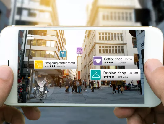
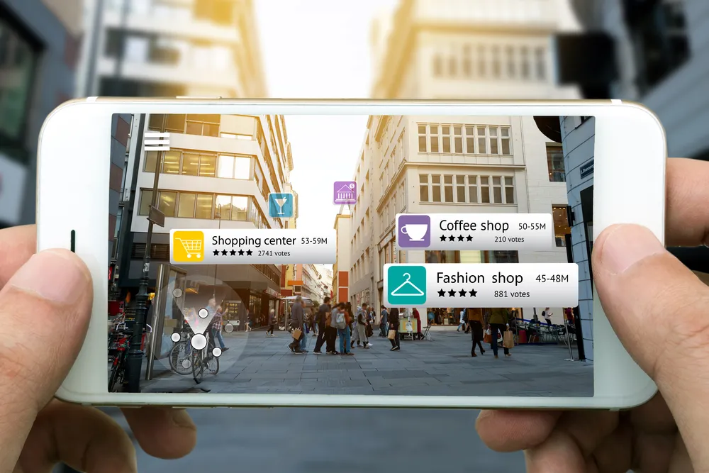
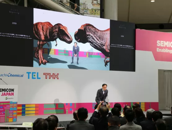
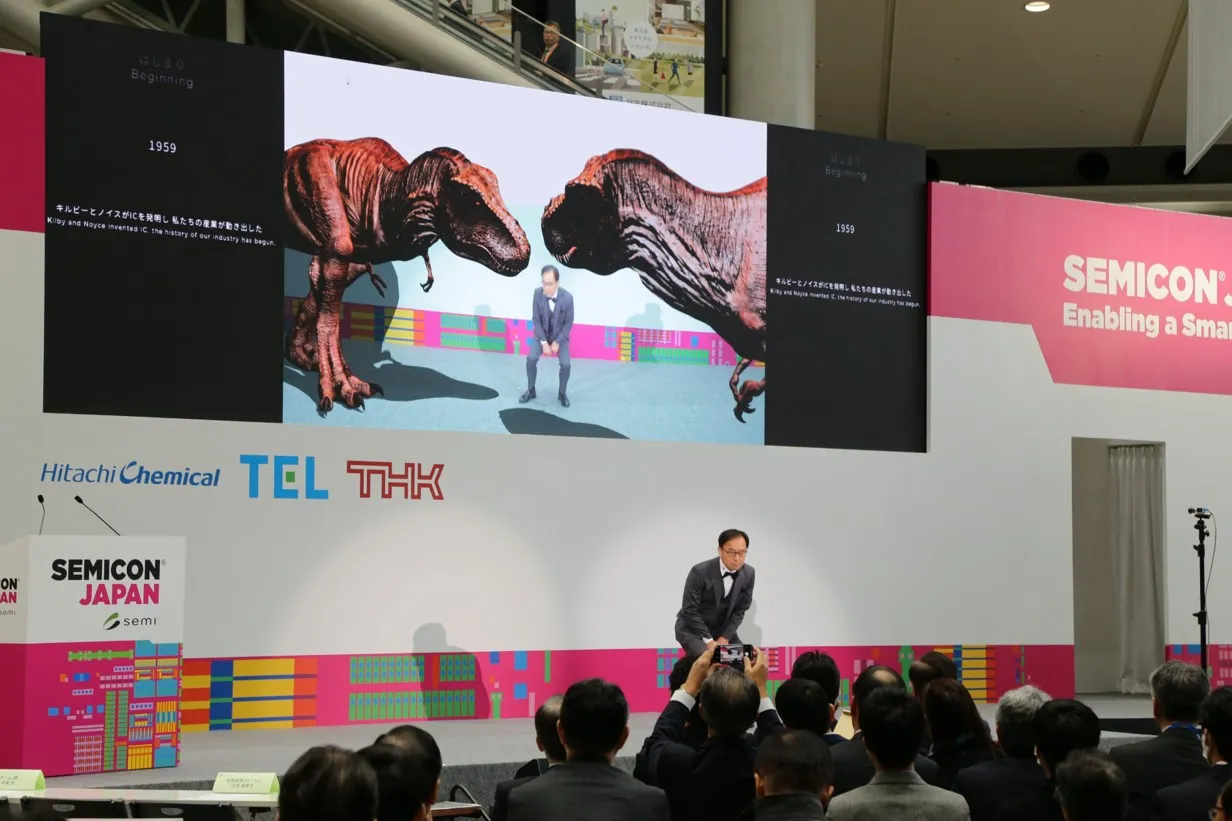
Augmented reality (AR) tyrannosauruses towered on-screen as I interacted with the creatures in a mix of prehistoric and cutting edge. Or, rather, my AR double was doing the playacting. Minutes later, virtual doppelgangers of a small lineup of chip industry executives cut the ceremonial ribbon. Seemingly sweeping away the winter chill, the opening of SEMICON Japan 2019 dazzled with smart technology and the promise of lives, cities and workplaces transformed, with uber-intelligent applications in full display at Tokyo Big Sight. But what resources does the industry need to harness to drive the next era of innovation? The semiconductor industry’s unwavering passion and young talent are key, said Hiroshi Imano, Chairperson of the SEMICON Japan Initiatives Committee, in his opening keynote. And hardly any region of the world is in a better position to help realize that future than Japan, Imano said. The region supplies one third of the equipment and more than half of all materials to the global semiconductor manufacturing industry.Talent was also top of mind for SEMICON Japan 2019 keynote speaker Makiko Eda, Japan's Chief Representative Officer at the World Economic Forum (WEF). Serving as a platform for public-private partnerships, the organization's mandate is to tackle global issues such as climate change and geopolitical strife in making world more resilient to risk and, by extension, more sustainable.Spanning ecology, economy, technology, society, geopolitics and industry, that mission includes reskilling and upskilling a billion people over the next decade, a high priority for WEF, which hosts a conference every January in Davos, Switzerland. The theme of this month's conference – Stakeholders for a Cohesive and Sustainable World – reflects the vital importance of building the international partnerships and global consensus necessary to achieving WEF's goals.One key to that sustainability will be technology and Arm, a global chip design company, will play a key role, with the company’s chips touching over 70 percent of the world’s population, Arm president Yuzuru Utsumi said in his keynote. Today, Arm is driving toward an ambitious goal: Ship 100 billion chips from 2017 to 2021 – the same number produced over the previous quarter century – by powering advances in mobile computing, server and networking infrastructures, and automotive applications.Arm’s innovation ecosystem of more than 1,000 partners will deliver these chips as they continue to work together to develop differentiated technology. Arm plans to increase investments not only in its primary processor business to accelerate market share gains but in the company’s new IoT business to create new revenue streams. The goal: Deliver long-term sustainable growth, Utsumi said. SEMICON Japan 2019 showcases SMART manufacturing and transportation Billed as a showcase of smart technologies, SEMICON Japan 2019 delivered with an array of eye-grabbing exhibitions in the popular SMART Applications Zone. In the SMART Transportation area, the automatic operation pavilion featured a car equipped with open-source software for autonomous driving. The exhibitor, Tier IV, aims to help lead the early commercialization of self-driving vehicles through the adoption of its software, Autoware, which makes it easier to develop self-driving vehicle prototypes using low-power platforms.Sony Semiconductor Solutions demonstrated a vision sensing processor designed to guide autonomous drones. Using two cameras, the processor measured the changing distance between visitors moving about the exhibit and stationary objects in real time, indicating proximity in hues of red (nearby) and blue (at a distance). Many visitors were wowed, describing the multichromatic display as futuristic.Others rode a simple wooden swing hanging by two ropes, but from dizzying heights thanks to Solidray’s Duo-Sight, a virtual reality (VR) system that projects 3D images stretching from wall to floor for immersive experiences. One visitor thrilled at how riding the swing, suspended only a few feet from the floor, felt like soaring on a flying trapeze. Target applications for the technology include virtual rides at amusement parks and presenting interior design options to homeowners.In the SMART Manufacturing area, one highlight was the demonstration by the National Institute of Advanced Industrial Science and Technology (AIST) of a remote-controlled Minimal Fab System designed for low-volume, high-mix chip production with little staffing. Designed to increase production efficiency, the system allows a circuit designer to manufacture a semiconductor by singlehandedly operating equipment up and down the production line. Controlling nearly 50 pieces of equipment, the Minimal Fab System on display manufactured chips that were verified for functional operation and exhibited afterwards.On the SMART Applications stage, exhibitors DENSO and Toyota Motor Corporation announced a new joint venture to conduct research and advanced development of the next-generation in-vehicle semiconductors critical to electric and autonomous vehicle innovation. The venture, operating as MIRISE Technologies, will combine Toyota’s mobility expertise with DENSO’s in-vehicle component prowess. The goal is to build a rapid, competitive development system by 2030, said Yoshifumi Kato, executive director of the DENSO Research and Development Center, and president and representative director of the venture. On track to begin work this year, MIRISE will span three fields of technology development: power electronics, sensing and SoC (System-on-a-Chip). The name MIRISE combines word the Japanese word "mirai" (future) with "rise."Business Continuity PlanningNatural disasters and other emergencies are an ongoing threat to uninterrupted business operations across the semiconductor manufacturing supply chain and particularly in earthquake-prone Japan. To better prepare for business disruptions and restore normal operations as soon as possible after disaster strikes, more companies are teaming on Business Continuity Planning (BCP).THK's Seismic Isolation Experience Car demonstrated one technology designed to help – a seismic isolation device. The car shakes like an earthquake to give people inside a taste of how a building heaves and sways during a quake with and without the device deployed. Visitors were struck by how much the isolator dampens tremors to prevent or minimize damage. In the BCP seminar, representatives from Sony Semiconductor Manufacturing, THK, DISCO and Team Engineering Consulting shared lessons learned from actual disasters and discussed the critical importance of daily disaster drills. Yukihide Keigo, Executive Engineer in charge of Products and Development at Sony Semiconductor Manufacturing, recounted how the company’s Kumamoto Prefecture plant struggled for 96 days to restore full operations after the facility sustained heavy damage in the 2016 earthquake. Keigo said the plant lacked the structural reinforcements necessary to withstand the impact and fell prey to poor planning and accountability. The Kumamoto plant has since implemented measures – structural and procedural improvements – that more accurately account for seismic risks to ensure full recovery within 56 days. The plant’s new procedures include emergency drills for staff including night-shift workers.Innovation abounds at six SuperTHEATER forumsSEMICON Japan 2019 was held in the West and South Halls of Tokyo Big Sight as organizers of the Tokyo Olympics occupied the East Hall, the exhibition's usual home at the venue, to prepare for the 2020 games. For the first time, the main stage, SuperTHEATER, was set up in the cavernous arena near the main entrance. The SuperTHEATER featured six forums over three days. Semiconductor Executive Forum – View by Top Two in the Era of Digitalization with thought leaders from IHS Markit and Sony Semiconductor Solutions SMART Connectivity Forum – Infinite World Brought by 5G Innovation with experts from Softbank and Nokia Solutions Networks SMART Transportation Forum I – Front-line of Automated Driving featuring speakers from Intel and DENSO SMART Transportation Forum II – Revolution of Sky Transportation, supported by the U.S. Commercial Service in Japan, with presenters from Ministry of Economy, Trade and Industry (METI), Subaru and Bell Helicopter Manufacturing Innovation Summit – Issues and Innovation: What will Drive Growth to 2030 featuring thought leaders from VLSI Research, Applied Materials, KLA, Nikon and Tokyo Electron Mirai Vision Forum – Future Relation of Technology and Body 2.0 with speakers from Leave a Nest, Ory Lab and Autonomous Control Systems Laboratory The Mirai Vision Forum highlighted advanced technologies that could lead to societal improvements. One presenter, Kentaro Yoshifuji, CEO at Ory Lab, recalled how, as a child, he once stayed home from school while recovering from an illness. His imagination in full flight, the youngster imagined having a clone that could attend school and be with his classmates. The experience eventually inspired him to develop OriHime, a robot that gives socially isolated people a way to communicate with friends or colleagues remotely. Originally developed for physically impaired people, OriHime today is used to help the able-bodied. The robot is situated with the companion and the user operates OriHime remotely. A camera and monitor in OriHime’s face provide the visual and audio connection and the user controls the device with a smartphone or tablet or, for those who are paralyzed, through eye movement. One potential application: With OriHime stationed at a business office, working mothers could use OriHime to telecommute to better balance their careers with their parenting responsibilities at home. The robot would be a mother’s go-between, enabling her to communicate directly with colleagues.The next generation of innovators also took the stage as five teams presented innovative business ideas in friendly competition. The top prize in The TECH CAMP Hackathon went to the group that hatched an ingenious plan to develop a jacket that trains users to move their bodies in preprogrammed ways. For example, legendary Japanese professional baseball player Shigeo Nagashima could wear the gear while batting to program the device, then give the jacket to someone who’s never swung a baseball bat. The jacket would help the user replicate Nagashima’s swing. Now comes the real work of any innovator – executing on the vision.And then came two soccer-playing artificial intelligence (AI) robots that squared off and ... Scored! The demonstration by the Toyota National College of Technology started as a research project by Toyota National College students in 2002. The young innovators designed and developed all the robotic hardware and software from scratch. Looking ahead to SEMICON Japan 2020!SEMICON Japan 2019 not only gathered leading Japanese semiconductor materials and manufacturing equipment providers to demonstrate their latest innovations. The premiere regional event also provided insights on key trends critical to the entire electronics manufacturing supply chain. This year’s event drew more than 51,000 visitors and 695 exhibitors from 15 regions filling more than 1,700 booths.SEMICON Japan 2020 returns to East Hall at Tokyo Big Sight in December 2020. I look forward to seeing you there!Jim Hamajima is president of SEMI Japan.
Read More
Have you ever wondered if you could “feel” what it’s like to revisit your favorite vacation spot while sitting on a couch in your living room? How about walk through a restaurant overlooking the water’s edge as you enjoy a savory dish, while still sitting on that couch?If you follow trends in consumer electronics, you probably imagined a virtual reality (VR) headset that uses a visual interface to simulate the ambiance of the restaurant as you use a voice interface to scroll through the restaurant’s menu. While the tech world has made great progress in evolving the visual and voice interfaces of VR, immersive virtual food-tasting also requires a digital interface that supports a sense of smell and taste. In fact, the National University of Singapore is conducting research on the topic (see the video), and Project Nourished claims to enable “eating and drinking in a whole new way – by hacking vision, gustation, olfaction, audition and touch – with or without caloric intake” – through VR.We’ve already come a long way in our quest to replicate human senses such as touch, vision (via biometric authentication) and voice to build user interfaces to interact with the digital devices around us. In fact, every invention that permanently changed the consumer electronics landscape in the last few decades has in turn brought to life one of these user interfaces (UI). For example, smartphones proliferated touch, video games such as Nintendo Wii and Sony Xbox brought gesture, and most recently, smart speakers and VR headsets have increased the adaptation of voice and vision.Complexities of UI DesignUI design is a complicated task that builds upon years of research in neuroscience, cognitive thinking and engineering. It must also account for individuality because users interact differently with their digital devices. Some, like me, use their left hand predominantly when interacting with a gaming console. Some have a heavy accent, which can make speech recognition difficult, while those with a hearing disability may prefer touch over voice as a user interface. Application, context and proximity of the device to the user also affect UI. For example, a user interacting with a smartphone at home has the option to touch or speak to the device whereas voice is the safest means to communicate with a car’s infotainment system while driving.Consumers often bring their digital devices wherever they go, but still expect a consistent user experience. Therefore, a natural user experience is the key to UI adoption. A multi-sensory approach combining voice, vision and/or touch could prove the most practical solution. For example, if I were to access my account at a bank ATM, I would prefer visual- or touch-interface authentication for security reasons, but I would still want to use a hands-free voice interaction to switch between the different menus on the machine. In this case, a combination of UIs could provide a more natural multi-sensory experience, albeit one that needs a careful design.UI technology development and adoption are largely influenced by the top four players in the consumer electronics industry – Apple, Amazon, Google and Samsung. Apple pioneered the touch interface with the invention of keyboard-less smartphones, and the rest of the industry followed suit. The introduction of Google Glass kickstarted the VR/augmented reality (AR) segment and opened new applications in the gaming and multimedia entertainment segments. While VR headsets work for gaming – and more recently for selling products and experiences – they are large and cumbersome devices that are uncomfortable to wear for extended periods. These are major hurdles for designers to solve. Voice, on the other hand, offers a hands-free user interface that is a more natural and frictionless compared to alternative UIs.A voice UI needs nothing but a voice command to interact with digital devices. However, it comes with its own complexity of varying user speech characteristics such as accent or volume. More importantly, the need to suppress various background noises for efficient use of voice UIs is critical. While edge computing and/or cloud-based artificial intelligence (AI) are critical technologies to enable battery life and performance of smart home devices, the overarching goal of conversational AI is still far from reality.From a business standpoint, the winner of the race for voice UIs must improve AI capabilities while supporting a strong ecosystem of partners. Amazon, for example, is king of this strategy. The e-commerce giant is building an Alexa Voice Service (AVS) ecosystem by way of its Alexa Fund companies and third-party integrations (partners) to realize its goal of proliferating voice everywhere. These partnerships enable the ecosystem to build end-to-end speech systems that can literally take voice interface products everywhere and promote, among other things, hardware startups that are disrupting the MEMS market with products such as environmentally robust piezoelectric microphones.Energy harvesting near-zero-power always-listening microphones, used in partnership with the AVS ecosystem, are enabling voice UI products to expand into battery-operated applications such as hands-free TV remotes, smart garbage cans, Bluetooth speakers, headsets, hardware appliances and automobiles. A good example of a unique voice UI launched at CES 2019: Housewares designer simplehuman’s voice-activated smart garbage can uses Vesper microphones and AVS. Watch the video.While the future might bring additional digital interfaces, along with multisensory experiences using vision, gesture and touch, voice UI is at the forefront of current technological innovation. Soon, Alexa might help cook dinner without intervention, even turning off the stove when food is burning through the use of a scent-detection sensor integrated with a microphone array. Voice UI continues to astound us with its possibilities, and we’re excited for the journey ahead.With more than 12 years of experience working in speech and voice applications for wireless devices, Udaynag Pisipati is a senior field applications engineer at Vesper. He holds a master’s degree in electrical engineering from University of Missouri and an MBA from Santa Clara University. A firm believer in speech as a natural user interface for human-machine interaction, Pisipati’s areas of interest include everything related to speech processing, including microphones/speakers, signal processing and machine learning.Vesper is a member of MEMS Sensors Industry Group (MSIG), SEMI technology community.
Read More
The 3D optical sensing market is once again surging – and it’s all thanks to Apple. What will we see in the next wave of end products enhanced by this technology, how will other market segments approach – and eventually use – 3D optical sensing, and which suppliers stand to gain the most from this very vital technology?Although 3D sensing, facial recognition and optical authentication systems have become only recently hot topics in the consumer electronics market, these mechanisms first made their appearance nearly a decade ago in November 2010. Following that debut, Microsoft soon launched the Kinect system in its Xbox 360 gaming console, marking a milestone as significant as Nintendo’s launch of its Nintendo Wii remote controller in 2010, which catapulted MEMS motion sensors into the high-volume consumer market.The Kinect system used a triangulation-based camera that Israeli developer PrimeSense Ltd. created and then licensed to Microsoft; Apple liked the technology so much that it acquired PrimeSense in 2013. The first version of Kinect applied the Structured Light (SL) method, a depth-sensing principle featuring an infrared (IR) laser projecting dots onto the scene, with a monochrome CMOS sensor measuring the differences in the acquired pattern. The second version of Kinect used the Time-of-Flight (ToF) principle.Kinect for Xbox360 was not only a successful consumer product; it also sparked a new market, thanks to the relatively low cost of the 3D sensing solution. By using the same hardware for Xbox 360 as in its first version of Kinect, Microsoft allowed developers to design their pet projects in the Kinect environment. Adding hand gestures controls to a PC, creating a user-controlled virtual dynamic light (see Kimchi and Chips’ demo), and developing an inexpensive hologram generator (see “Princess Leia” video from the MIT Media Lab) are just a few examples of ecosystem developers and DIYers applying their creativity to Kinect.Apple Goes 3D with Face ID3D optical sensing has expanded from gaming consoles to the smartphone. In 2017 Apple presented its Face ID camera system for the iPhone X, which they launched to celebrate the 10-year anniversary of the iPhone. Face ID is the result of a longer term strategy for Apple, the byproduct of several company acquisitions to expand know-how in 3D sensing and augmented reality (AR)/virtual reality (VR). Between 2015 and 2018, Apple acquired the camera-module maker LinX (2015), the AR startup Vrvana and the imaging sensor firm InVisage Tech (both in 2017), and AR glasses’ designer Akonia Holographics (2018).For a company that has always innovated on its own terms, Apple’s idiosyncratic approach called for deployment of the Structured Light method combined with a ToF device. The result is an amalgamation that utilizes the best features of the two mechanisms, even if the combination is one that is expensive. Apple’s addition of a near-infrared illuminator to its ToF device enhances the system’s effectiveness under most light conditions while also improving the reliability of Face ID; the overall outcome is a more satisfying user experience. The ToF component, which STMicrolectronics supplies, makes use of so-called single-photon avalanche diode (SPAD) receivers that can work with any target material and color, although a higher target illumination is required to obtain good accuracy.The other core components of the Face ID system are the Vertical Cavity Surface Emitting Laser (VCSEL, from Lumentum) and a dot projector (from ams/Heptagon), assembled together in an optical package. Apple’s expensive but reliable approach explains the company’s inclusion of the Face ID system in its latest smartphone and tablet offerings – across the iPhone Xs, Xs Pro and Xr as well as in the latest iPad Pro models. Apple’s Face ID uses facial recognition for authentication on a range of iPhone and iPad Pro models. Image courtesy of Apple. Chinese Phone Makers Get into the GameMeanwhile, other mobile handset manufacturers are rumored to be working on Face ID-like systems or have already presented similar solutions, albeit through a variety of approaches. Some have chosen to use standard ToF devices while others have adopted an SL tactic. In many of these designs, which happen to target Android systems, OEMs generally include a fingerprint sensor as a fallback biometric option to their own nascent 3D facial recognition systems. The fingerprint sensor operates in either standalone mode or integrates into the display.Chinese handset maker Oppo, for instance, uses the SL method on its Find X model with algorithms coming from Megvii. Oppo claims its equivalent of Apple Face ID is faster. I have heard that Vivo has been working on a ToF camera since mid-2018, which it claims provides greater accuracy and security in end-applications such as secure payments and unlocking the phone.Chinese technology giant Huawei’s first 3D facial sensor appeared in its Mate 20 Pro flagship mobile phone. Aside from providing facial biometrics, the front-facing 3D sensor doubles as a 3D scanner, enabling users to digitize live objects that they can then manipulate in 3D AR applications. While still a novelty, the application highlights the use of 3D light sensors beyond that of biometrics. Xiaomi’s Mi Explorer Edition smartphone features a complex SL 3D module to enable 3D facial scanning although it looks like a clone of the Apple solution.Overall, the importance of facial recognition is no longer a matter of dispute, given that Apple’s rivals are now developing counterpart offerings of their own. Leaked code from the next revision of the Android operating system (revision Q), now under development by Google, has confirmed as much. Big and Getting BiggerIHS Markit forecasts that global revenue for ToF sensors in the 3D optical sensing market will surpass $500 million in 2019, up from $370 million last year. We also predict that the ToF market will grow in the coming years, spurred by combo solutions integrated with other light sensors in the same package. This will lead to a cheaper bill of materials (BOM) compared to the BOM for the SL method.At the same time, IHS Markit forecasts that the total market potential for light sensors will be worth much more, reaching $1.5 billion by year 2022. That’s because after a solid start with gaming consoles, 3D sensing has matured and consolidated in the massive smartphone arena.A segment of 3D Sensing’s future growth will come from other use cases and applications that are emerging outside consumer electronics and mobile. These include people-counting and -tracking in consumer and industrial applications, landing-aid and obstacle-avoidance functions in drones, and car-trunk (boot) opening with foot gestures, as well as gesture recognition and passenger detection in automotive. IHS Markit predicts steady growth for ToF and other light sensors. All told, the ToF approach appears to have a greater chance than the SL method in gaining a larger market share, leading to a cheaper and smaller BOM along with reduced integration costs in system assembly and calibration.Sometime this year, Apple and other handset OEMs may include a ToF-based 3D camera on the back of the iPhone to support more immersive gaming experiences and new AR/VR applications. This will further boost the 3D sensing market.To be sure, other mature technologies are available as valid alternatives to optical 3D sensing, including ultrasonic, mmWave and radar. These alternative technologies may gain part of the total market now commanded by 3D sensing, in use cases such as obstacle-avoidance or in-cabin presence detection.To learn about 3D Optical Sensing and Light Sensors from IHS Markit, go to: https://technology.ihs.com/606483/light-sensors-for-consumer-mobile-report-2018Manuel Tagliavini, a principal research analyst at IHS Markit, covers MEMS and sensors technology.Manuel Tagliavini joined IHS Markit in 2017. His key areas of focus are MEMS and sensors for mobile and consumer technologies. He is responsible for the tracking of sensors in handsets, tablets, laptops, and sports and fitness products.Prior to IHS Markit, he spent over 10 years with STMicroelectronics, working in various roles including product engineering, program management, and marketing and business development in the company's MEMS division.Tagliavini earned an Executive Master of Business Administration at SDA Bocconi School of Management and a Master of Science in Electronic Engineering from the University of Parma, both in Italy.Stay tuned with the technological advances and market trends in the MEMS Sensors ecosystem. Join MEMS Sensors Industry Group (MSIG), the SEMI technology community that connects the MEMS and sensors supply network in established and emerging markets, allowing members to grow and prosper.
Read More