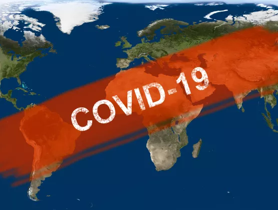
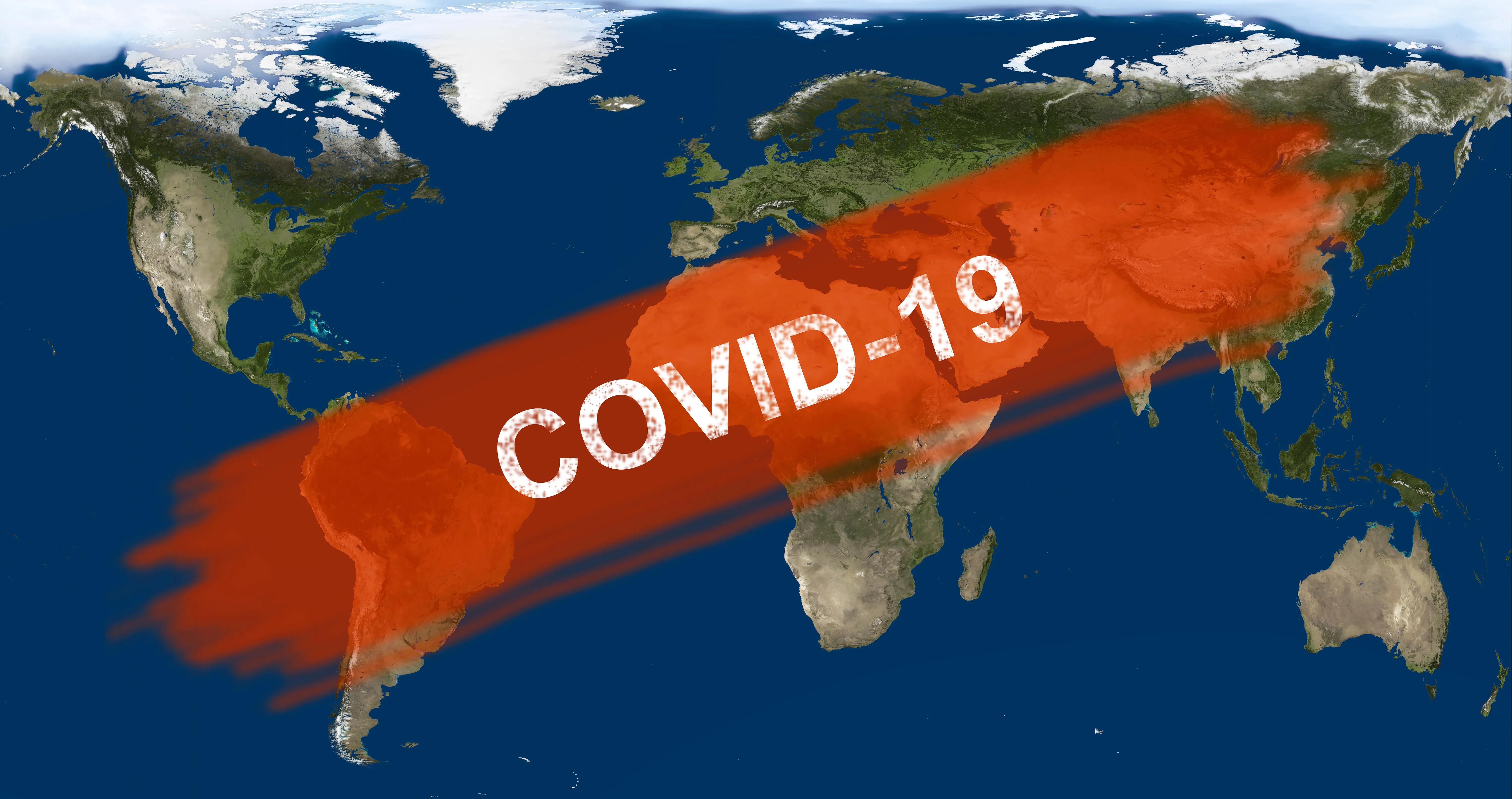
The pandemic unleashed by the coronavirus SARS-CoV-2 (which causes the disease COVID-19) has infected over 100 million and resulted in over 2.6 million deaths worldwide as of March 2021. It is well-established that this virus primarily spreads from person-to-person via respiratory droplets produced when an infected person coughs, sneezes or even breathes (see Ref. 1-3). Subsequently, the droplets meet the eyes, or enter nose or mouth of a nearby person, or transmit when a person touches an infected surface, then contacts their eyes, nose, or mouth.
Since the virus is small, 0.06–0.14 microns in diameter, many copies can be contained in or attached to emitted respiratory droplets. Droplets as small as one micron can carry enough viral load to cause an infection. A particular concern is the interaction of droplets with ventilation systems, which potentially could enhance the propagation of pathogens. This has implications on situation-specific safe distancing and the design of building filtration systems, air distribution, heating, air-conditioning and decontamination systems. A particular instance of this is the semiconductor manufacturing cleanroom, where systems and protocols are specifically designed to minimize contamination.
The $440 billion global semiconductor industry depends on these cleanrooms for integrated circuits (chips), and in turn, these chips form the lifeblood of the multi-trillion-dollar global electronic systems industry. Electronic systems are now critical for just about every aspect of human life, including health, work, finances, entertainment, transportation, power grids and many others. Thus, it is critical to understand how cleanrooms can operate more safely to ensure the health of workers while maintaining productivity levels to meet increasing global demand for semiconductors. In the work described here, we analyzed particle and droplet transport via modeling, simulation [Refs 1-3], and experimentation [Ref. 4] to help guide the industry.
Modeling and Simulation
In this part of the work, mathematical models were developed to simulate the progressive time-evolution of the distribution of locations of particles produced by a cough. Analytical and numerical studies were undertaken. The models ascertain the range, distribution and settling time of the particles under the influence of gravity and drag from the surrounding air. Beyond qualitative trends that illustrate that large particles travel far and settle quickly – versus small particles that do not travel far and settle slowly (yet can be carried far by ambient flow) – the models provide quantitative results for distances travelled and settling times, which are needed for constructing social distancing policies and workplace protocols. Figure 1 shows examples of the results of the modeling and simulation work.
Figure 1: Model of particle spreading from a person coughing, with and without a mask.
(Ref. 1)
Following are key insights from the modeling and simulation work (Ref. 1):
Large particles travel far (launched “ballistically”) and settle quickly, while small particles do not travel far and settle slowly (when there are no ambient externally-driven flow fields).
Small particles do not settle even by the end of the simulation time (4 seconds in Ref. 1). Accordingly, the simulations were also run for extremely long periods to ascertain that the “mist” of small particles remained airborne for several minutes (as predicted by the theory). For strong opposing headwind, small particles move backwards, yet still remain airborne for extended periods of time. This is by far the most dangerous case since this will encounter other persons at the torso level.
Ratio of the general drag to gravity indicates that at high velocities, the dynamics are dominated by drag.
For general cough conditions, there can be cases where the change in the surrounding fluid’s behavior, due to the motion of the particles and cough, may be important.
One major implication of this work is that the challenge of infection must be addressed both spatially and temporally. In other words, it is necessary to maintain social distancing based on how far the virus travels, but it is also important to account for how long the virus stays at the location because of specific air patterns. On the positive side, understanding these spatio-temporal patterns accurately will enable companies to design (or re-design) ventilation and decontamination systems precisely to improve worker safety. Other aspects of this analysis entail contact tracing (Ref. 2) and decontamination (Ref. 3). Further details, including simulations, are available at https://msol.berkeley.edu/publications/.
Experimentation
The major vector of coronavirus spread is through respiratory droplets expelled when coughing, speaking, and breathing; and the efficacy of any safety measures depends on accurate characterization of the dispersal of these droplets. The term particle describes objects that begin their journey as a solid. The term droplet is reserved specifically for objects that are initially liquid, albeit it is important to note that droplets can evaporate and effectively transform into solid particles composed of non-evaporative material.
A purpose-built room, the Cal Covid Cube, C3, was set up and utilized for this research [Thatcher et al. 4]. The C3 is a parallelepiped room that is 232 centimeters tall, 376 centimeters long and 284 centimeters wide on the inside. For experimental results to be meaningful and repeatable for scientific and practical purposes, it is essential that the experimental setup be carefully controlled and calibrated. The following precautions were taken to ensure this:
Charge-free: When solid particles are released, it is critical to eliminate (or thoroughly know) static charge effects for obtaining accurate deposition patterns. Static charge effects can manifest through particle-particle interactions (affecting particle motion in flight) or particle-surface interaction (affecting deposition pattern). Two methods for the elimination of charge effects on the deposition surface were found to be effective: (1) ionized non-conductive adhesive sampling strips, and (2) grounded aluminum backed carbon sampling strips.
Isothermal: The room is a converted walk-in freezer with 10.5-13 centimeter thermal insulation and located in the middle of a building, at least 5 meters away from all building walls. Temperature uniformity was checked and the C3 room temperatures were found to be isothermal within uncertainty of measurements.
Quiescent: It was ensured that the room did not create uncontrolled thermal convection due to isothermal nature. Quiescence was verified with both hot-wire measurements and with free-falling particle drift observations.
Isopotential: The outer and inner surfaces, including the door of the C3 were conductive aluminum and stainless steel, and copper tape were used to ensure reliable electrical connection of door, interior and exterior panels. Electric fields were surveyed and found to be negligible within precision of instruments.
Other design elements: All interior surfaces were coated with black matte paint to reduce scattered light and provide uniform background for imaging measurements. The facility was located on ground floor to limit vibrations.
Repeatable Launch: To emulate the release from a true cough or sneeze, and to better understand droplet motion in a canonical turbulent jet versus a cough type release, we studied different layers of complexity for the release geometry:
(i) Straight round pipe
(ii) Smooth 90-degree curved pipe, with a changing radius along the length of the pipe
(iii) Intubation trainer doll, with realistic airways and mouth/tongue structure
Figure 2 shows the experimental setup with the intubation doll in C3, with the particle/droplet release being measured after deposition on the sampling strips that appear green.
Figure 2: Experimental Setup in C3 with both charge neutralized (white appearing green) and conductive (black) sampling strips placed on a conductive and grounded alignment grid [Ref. 4]
We utilized both liquid droplets and solid particles. For droplets, we explored and found promise in a method of deposition analysis based on fluorescence. For particles, we explored many ways in which the smallest of thermal gradients or electrostatic charge issues can affect the data and developed practical methods to address these issues. For accurate measurement free of static charge effects even in environments where high ambient flow velocities may cause a nonconductive surface to rapidly acquire charge (e.g., clean room environment), we developed carbon-tape-based sampling strips that are cleanroom-compatible, conductive, and grounded. For analysis, we developed a cost-effective method utilizing a commercial photo negative scanner followed by image enhancement by blind deconvolution. Figure 3 shows sample results for particle deposition location along our centerline for particles in the ballistic, intermediate and aerosol regime.
Figure 3: Experimental Results [Thatcher et al. 4]
Following are key insights from experimental work:
Significance of both static charge effects and thermal gradients in rooms for validation tests are more than usually appreciated.
For modelling, accounting for the non-uniform initial particle velocity matters for the ballistic particles.
For all sizes of particles, simulating the transient versus steady state significantly impacts predicted particle spread.
Thermal plumes alone from humans along particle flight path can transport 50 micron particles across the room. In some situations, this was observed up to ~6 meters.
There is a significant effect of Relative Humidity (RH) and temperature on droplet evaporation. The practical consequence is that, in low RH, particles spread further, with all other things being equal. (The reason is that particles shrunk more and entered the aerosol regime.)
In summary, a systematic analysis of particle and droplet transport was conducted by simulation, modeling, and experimentation. We were able to develop robust, rigorous, and repeatable methodologies and draw meaningful insights that will support safer operation and productivity of semiconductor cleanrooms globally. Further, these studies will help with the design (or re-design) of ventilation and de-contamination systems that help protect both the health of humans and the economy from current and future pandemics. This article provides a high-level overview of the work, and further details will be available through a series of scientific papers that are in various phases of publication.
We gratefully acknowledge the following support:
Gift of the Lam Research Corporation
Gifts coordinated through SEMI and provided by Advanced Energy Industries, Applied Materials, ASM, Entegris, JSR, KLA, TEL, and Wonik
The 2020 Seed Fund Award from the Center for Information Technology Research in the Interest of Society (CITRIS) and the Banatao Institute at the University of California
Vision Research for providing a v2640 camera to help quantify the particle velocities
Graduate students Eric Thacher and Tvetene Carlson who conducted the experiments in C3
Valuable discussions with Brett Singer, Thomas Kirchstetter, Michael Sohn, Chelsea Preble of Lawrence Berkeley National Laboratory regarding droplet transport and COVID, and Keith Hansen on particle sampling and charge neutralization
DOE Office of Science through the National Virtual Biotechnology Laboratory, a consortium of DOE national laboratories focused on response to COVID-19, with funding provided by the Coronavirus CARES Act
Steven Ruzin and the Biological Imaging Facility for their assistance in obtaining the high-quality fluorescence microscopy scans to validate the particle counting methodology.
References
Zohdi, T.I. (2020) Modeling and simulation of the infection zone from a cough, Computational Mechanics. https://doi.org/10.1007/s00466-020-01875-5
Zohdi, T.I. (2020). An agent-based computational framework for simulation of global pandemic and social response on planet X, Computational Mechanics. https://doi.org/10.1007/s00466-020-01886-2
Zohdi, T.I. (2020) Rapid simulation of viral decontamination efficacy with UV irradiation. Computer Methods Appl. Mech. Eng. https://doi.org/10.1016/j.cma.2020.113216
Thatcher, E., Carlson, J., Castellini, J., Sohn, M.D., Variano, E. and Makiharju S.A. (2021) Droplet and Particle Methods to Investigate Turbulent Particle Laden Jets (in preparation)
Authors
Evan A. Variano, Professor, Environmental Engineering, UC Berkeley
Simo Mäkiharju, Assistant Professor of Mechanical Engineering, UC Berkeley
Tarek I. Zohdi, Will C. Hall Endowed Chair of the UCB Computational Data Science Engineering Program, Professor of Mechanical Engineering, UC Berkeley
Pushkar P. Apte, Director of Strategic Initiatives, Center for Information Technology Research in the Interest of Society (CITRIS) and the Banatao Institute, UC Berkeley; and Strategic Technology Advisor, SEMI