downloadGroupGroupnoun_press release_995423_000000 copyGroupnoun_Feed_96767_000000Group 19noun_pictures_1817522_000000Member company iconResource item iconStore item iconGroup 19Group 19noun_Photo_2085192_000000 Copynoun_presentation_2096081_000000Group 19Group Copy 7noun_webinar_692730_000000Path
Skip to main content
Default Banner Image

Intel

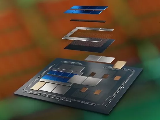
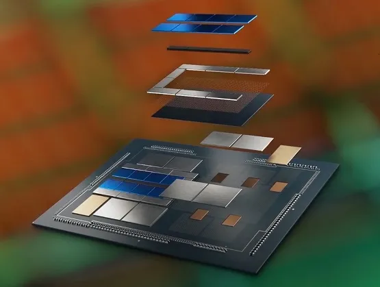
As monolithic scaling slows down, the semiconductor industry is increasingly relying on advanced packaging technologies to extend Moore’s law through heterogeneous integration. Higher on-package bandwidth, improved yield resiliency and the need to integrate diverse IP from multiple foundries are driving demand for advanced packaging technologies that address these issues but introduce challenges of their own such as efficient power delivery to all the different domains in a heterogeneous system. SEMI spoke with Kaladhar Radhakrishnan, Intel Fellow at Intel, about heterogeneous system integration trends and new developments in the semiconductor industry. Radhakrishnan shared his views ahead of his keynote at the SEMI Connecting Heterogeneous Systems Summit, 1-3 September 2021, an online event. Join the summit to meet experts from Intel and other key industry influencers. Registration is open. SEMI: What is driving the adoption of electronics and semiconductor devices nowadays and why is the development of new and innovative technologies important? Radhakrishnan: We are living in an increasingly data-driven world where devices have become an integral part of our lives. A recent study estimated that in the United States alone, 13.6 connected devices per capita consume an average of 300 gigabytes worth of data every month. In the workplace, COVID-19 has driven fundamental business changes that has sped up the adoption of digital technologies such as virtual conferencing, remote work, and e-commerce. Organizations are realizing that a high-quality video conference can be an adequate substitute for many in-person meetings. As a result, businesses are accelerating the digital transformation in order to adapt and thrive in this new environment. Five decades of sustained exponential growth in semiconductor performance has conditioned the average digital consumer to expect more from their devices. However, there are some headwinds ahead as traditional scaling slows down and power density rises. Because consumers and businesses are now generating data at a faster rate than they can consume it, technologists need to scale compute, storage, and bandwidth even faster to keep pace. Without investments in research and development of new and innovative technologies to address these challenges, the full potential of this data will go unrealized. SEMI: What forces are heightening the importance of heterogeneous system integration? What are the implications for increased on-package bandwidth, improved yield resiliency and the need to integrate diverse IP from multiple foundries? Radhakrishnan: The semiconductor industry increased transistor density and scaled performance through classical Dennard scaling until the turn of the century. By then, the gate oxide thickness had scaled down to atomic dimensions and the exponential increase in sub-threshold leakage signaled the end of scaling through traditional methods. Since that time, the chip industry has been relying on innovations in transistor materials and structures such as high-k metal gate, strained silicon, and FinFETs to keep pace with Moore’s law. However, this alone will not be sufficient to continue scaling and the industry needs to explore other vectors to augment improvements in transistor technology. Heterogeneous integration through advanced packaging is one key technology that can help drive these gains. Technologies like Foveros can enable device density scaling by creating a 3D stack of multiple die using high-density interconnects. Heterogeneous integration enables chipmakers to move from a monolithic system designed on a single large chip to a heterogeneous system comprised of a number of smaller chiplets. The main benefit of using smaller chiplets is that they improve yield and enable application based customization of the foundry processes. However, if the disaggregation to smaller chiplets is not accompanied by an increase in on-package bandwidth, the power and performance penalties associated with chiplet-to-chiplet communication will hobble system performance. This is why advanced packaging technologies that improve die-to-die communication are key enablers for heterogeneous integration. SEMI: What are some of the key technology challenges in developing heterogeneous systems? Radhakrishnan: The obvious challenge that most people focus on is the need for improved on-package bandwidth. However, as we rely on 3D stacking to continue device scaling at the package level, it is important to comprehend power delivery and thermal challenges as well. Power to the top die has to be delivered through TSVs on the bottom die, which not only adds resistance but also reduces the useful area available on the bottom die. This problem is further exacerbated when we stack more than two die. Excessive noise on the power delivery network can cause timing issues that limit the maximum operating frequency of the transistor. Similarly, when we stack multiple die, we must take into account associated thermal challenges. For example, each interface of the multi-die stack adds thermal resistance, which makes it harder to cool the chips at the bottom. SEMI: What are some of the key global market trends that driving demand for heterogeneous and system-level integration? Radhakrishnan: The number of artificial intelligence (AI) and machine learning applications have grown dramatically due to their ability to solve highly complex problems across a wide range of segments. AI and machine learning models require more memory bandwidth and compute capabilities that are difficult to achieve without some form of heterogeneous integration. Another market trend driving demand for heterogeneous integration is the increasing reliance on custom hardware accelerators. To combat the slowdown in frequency scaling and single-core performance, we have moved to multi-core architectures by tackling the inherent parallelism in our workloads. However, Amdahl’s law tells us that such an approach will hit a bottleneck when we reach the limits of the serial portion of the workload. As these constraints slow the performance of general-purpose processors, the reliance on custom hardware accelerators to boost performance for specific workloads is growing. Heterogeneous integration at the system level with a combination of CPUs, GPUs, FPGAs and other accelerators can optimize system power and performance. SEMI: What solutions is Intel developing to address these market needs? Radhakrishnan: Intel is actively involved in the development of the industry ecosystem for heterogeneous integration. We have developed a number of innovative advanced packaging solutions such as the EMIB and Foveros that are used in products today. Intel is also developing the next generation of advanced packaging technologies, Foveros Omni and Foveros Direct, which will dramatically scale the IO density by using direct Cu-Cu bonding technology. Foveros Omni is a crucial building block technology to enable high-voltage power conversion on the package for efficient power delivery. Intel is uniquely positioned to predict the design needs for future systems and deploy its resources to develop the technology building blocks needed to continue performance scaling. Our IDM 2.0 strategy enables us to leverage our leadership in packaging technologies to design the best products and use the best IP to deliver leading products across a broad range of categories. SEMI: What do you expect from your participation at SEMI Connecting Heterogeneous Systems Summit? Radhakrishnan: I’m hoping to shed some light on some of the new technologies we have been developing at Intel to enable heterogeneous system integration. I also want to bring awareness to the power-related challenges we are facing with heterogeneous systems. I also look forward to listening to what other industry leaders have to say on the topic. Kaladhar Radhakrishnan is an Intel Fellow and a Power Delivery Architect with the Technology Development group at Intel. He plays a significant role in shaping and driving power delivery technologies for Intel microprocessors. His areas of expertise include integrated voltage regulators, advanced packaging and passives technologies. Kaladhar is a two-time recipient of the Intel Achievement Award, the highest Intel honor an individual or small team can receive. He has authored four book chapters, over 40 technical papers in peer-reviewed journals, and has been awarded 35 U.S. patents. He has also served as an adjunct professor at Arizona State University. Kaladhar joined Intel in 2000 soon after receiving his Ph.D. in Electrical Engineering from the University of Illinois at Urbana-Champaign. Serena Brischetto is senior manager of marketing and communications at SEMI Europe.
Read More
The state of Penang, nestled along the northwest coast of Peninsular Malaysia, needs no introduction in the global electronics manufacturing sector. Despite its diminutive stature with just over 1,000 square kilometers of land area and a 1.8 million-strong population, Penang commanded an estimated 5% of global semiconductor exports in 2019, according to data compiled from the Department of Statistics Malaysia (DOSM) and UN Comtrade. The State’s transformation, from a traditional seaport economy into the Silicon Valley of the East, began in the 1970s, when the establishment of Malaysia’s first free trade zone in the State drew key investments from eight Multinational Corporations (MNCs). These pioneering investors – Intel Corporation, Hewlett Packard (now Keysight Technologies and Agilent Technologies), Robert Bosch, AMD, Litronix (now Osram Opto Semiconductors), Hitachi (now Renesas), Clarion and National Semiconductor[1] – sparked the development of a robust ecosystem of ancillary industries, which formed a foundation for the State’s rise as a prominent, offsite manufacturing hub. Today, Penang houses more than 350 MNCs that are supported by over 3,000 manufacturing-related SMEs. As Penang flourished as a vibrant, regional E E manufacturing hub, the local talent pool steadily accumulated a wealth of business intelligence and technical experience, enabling the robust supply chain to evolve in tandem with technology megatrends. This, in turn, enabled the State to focus on pursuing investments that have propelled the industry up the value chain, away from its beginnings as a low-cost manufacturing hub. Consequently, Penang has seen a proliferation of upstream technology-related investments in high value-added functions in recent years, ranging from research and development (R D), design and knowledge-based solutions, and downstream advanced manufacturing and testing to global business service (GBS) and Centre of Excellence (CoE) activities. Penang’s growing significance in the global E E value chain is demonstrated by its steady and resilient export performance in recent years. From 2014 to 2019, the State’s E E exports grew at a compounded annual rate (CAGR) of 12% to reach RM210 billion (US$51 billion). It has emerged as a hub for professional, scientific and controlling instruments (including medical technology), with exports of these products growing at a 5-year CAGR of 15% to reach RM23 billion (US$6 billion) in 2019. E E products, alongside professional, scientific and controlling instruments, collectively contributed between 77% and 82% of Penang’s total annual exports since 2014, and accounted for 50% of Malaysia’s exports in these two segments during the period. More impressively, despite the disruptions from the COVID-19 pandemic, Penang’s total exports continued to rise in 2020, growing 7% year-on-year to RM310 billion (US$75 billion), and a further 14% year-on-year in January and February 2021, driven by strong global demand for semiconductors. Shaping up as the destination of choice for advanced manufacturing investments As part of efforts to move Penang’s industry up the value chain, the State government has placed emphasis on attracting companies with strong commitments in implementing Industry 4.0 and sustainable investing. These efforts have yielded positive results, with the state having gained traction as a hub for advanced manufacturing investments. This is evidenced by the rising trend in investments per new job creation, which saw a six-fold jump from 2012 to 2020, as well as the number of global heavyweights announcing new investments as well as expansions of existing facilities in the State in 2019 and 2020. Penang attracted RM31 billion (US$7.5 billion) in approved direct manufacturing investment inflows in 2019 and 2020, 88% of which involved investments into the E E, equipment and medical technology industries. Prominent new investments included those from Lam Research, Bosch Group, Ultra Clean Holdings, Dexcom as well as Smith+Nephew. Together with planned expansions by a number of existing MNCs in Penang, these new investments, which are on track to commence operations between 2021 and 2023, are poised to bring Penang’s industry to greater heights and further integrate the State into the global value chain. Recent Notable Direct Manufacturing Investments in Penang Source: InvestPenang and respective companies Penang’s conducive business environment nurtures successful homegrown technology companies Penang’s conducive business environment has not only proven successful in attracting foreign direct investments (FDIs), but also successfully nurtured local E E success stories of locally employed engineers turned technopreneurs, who have founded and built companies that have successfully grown to become internationally renowned in their own right. These homegrown E E companies play crucial roles in the ecosystem, particularly in the areas of automated test equipment (ATE), automation, outsourced semiconductor assembly and testing (OSAT) services, electronics manufacturing services (EMS), precision engineering and tooling. The past five years have also seen the emergence of young, fast-growing Penang-based companies such as Experior, Oppstar Technology and Skyechip, which provide IC design and IC test design services to MNC clients globally. Public-private partnerships cultivate Penang’s talent development roadmap The state is cognisant that the development of a robust and skilled talent pool is imperative to support the growth of strategic industries in Penang. Strong public-private partnerships with concerted efforts in supporting talent development are key to Penang’s continued success. Toward this end, the State government has backed Penang Skills Development Centre’s (PSDC) industry-led training and education efforts, which have helped train over 200,000 of workers to support the industry’s needs since 1989. The State has also coordinated collaboration for industries to provide input to local institutions of higher learning on the relevance of the institutions’ courses, and rallied the industry to support State-run scholarships (Penang Future Foundation) and STEM initiatives. Holistic initiatives to make Penang a world-class investment destination for global frontier companies The dynamics of the global value chain, especially for the technology sector, have evolved rapidly since 2018, particularly amid the complex confluence of trade protectionism, COVID-19 pandemic-driven issues and disruptive technologies. The State government believes that strong, geographically localised industry clusters could help companies mitigate the risks of supply chain disruptions, in addition to improving companies’ time-to-market at a lower cost. To further increase Penang’s attractiveness for high quality investments, the State is focusing on three key strategies: Extending its competitive edge in advanced manufacturing, further strengthening Penang’s industry clusters, which include expediting SMEs’ Industry 4.0 transformation journey, and nurturing more homegrown companies to penetrate the global supply chain Embarking on a continuous drive to develop and recruit talent to the State, as well as cultivate the younger generation’s interest in STEM Enhancing Penang’s liveability with a strong focus on making Penang a smart and green city The State government is committed to continue developing Penang in a holistic manner, with the aim of creating a vibrant business and investment destination with a robust and sustainable economy and high standard of living, creating a conducive environment to “work, live, learn, play and invest.” About InvestPenang InvestPenang is the Penang State Government’s principal agency for promotion of investment. Its objectives are to develop and sustain Penang’s economy by enhancing and continuously supporting business activities in the State through foreign and local investments, including spawning viable new growth centres. To realize its objectives, InvestPenang also runs initiatives like the SMART Penang Centre (providing assistance to SMEs), Penang CAT Centre (for talent attraction and retention) and i4.0 seed fund (a catalyst for the start-up ecosystem). For more information, contact [email protected]. InvestPenang also works closely with various industry associations, including SEMI, to promote Penang’s supply chain and E E ecosystem. InvestPenang is delighted to have collaborated with SEMI on numerous occasions since 2015 and endeavours to sustain the partnership in the years to come, including for the SEMICON SEA 2022 exposition to be held in Penang. [1] No longer present in Penang following a corporate M A exercise.
Read More
What does it mean to identify as LGBTQIA+ in the semiconductor industry? It’s an interesting question to ask, but a difficult one to answer. Because we live in a world in which cisgender heteronormity is assumed, it’s possible to self-identify as LGBTQIA+ without sharing that information publicly. Coworkers and managers might not even realize that their colleague or employee is gay, lesbian, transgender, non-binary or other. Unlike other minorities, notably people of color, LGBTQIA+ people may choose to keep their identities invisible.As I began outreach for this article, I recognized that some people might not want to expose a potential vulnerability to both their co-workers and a broader global audience of SEMI members, so I tried to make them feel more comfortable. I told them I’m a lesbian. I said that I’d send content for their review before publishing. But I quickly discovered that wasn’t enough, despite sweeping cultural and legal advances around LGBTQIA+ attitudes and identity. According to a 2020 Gallup Poll, 5.6% of U.S. adults now identify as LGBTQIA+, up from 4.5% just three years ago. In 2004, Massachusetts became the first U.S. state to legalize same-sex marriage, and in 2015, the U.S. Supreme Court made same-sex marriage legal in all 50 states. The semiconductor industry has been historically conservative. The times, however, are changing. Large chip companies such as AMD, Intel and Lam Research actively support diversity and inclusion efforts across minority groups, including LGBTQIA+, and that’s a good thing, but is it enough? And if not, what actions can SEMI members take to help LGBTQIA+ people in semiconductors feel safe enough to choose visibility?According to Antoinette Hamilton, global head of Inclusion and Diversity at Lam Research, more than 46% of LGBTQIA+ employees in the industry aren’t out in the workplace. That tells us there’s still work to be done, a challenge that Lam is embracing. With its Pride employee resource group (ERG) leading the way, partnerships with organizations such as PFLAG and Out Equal, and recruitment efforts made through organizations such as Out in Science, Technology, Engineering, and Mathematics (oSTEM), Lam has earned a score of 100 on the Human Rights Campaign Foundation’s Corporate Equality Index and was named one of the Best Places to Work for LGBTQ Equality.“At Lam, we understand the importance of empowering employees to bring their authentic self to work,” says Hamilton. “We believe when employees feel valued and included, each person can reach their full potential.”Back in 1992 when Intel paid to relocate Judi Goldstein, her partner and their son from New Jersey to Oregon, mainstream cultural attitudes toward gays and lesbians were very different. According to a June 1992 Gallup poll, only 48% of Americans thought that “gay or lesbian relations between consenting adults should be legal,” with 44% saying they should be illegal. A May 2020 Gallup poll recorded a dramatic shift in attitudes, with 72% affirming the legality of same-sex relations and only 24% opposed.By the late 1990s, Intel had extended domestic partner benefits to same-sex couples. “I registered my partner – now my wife – and our son, and realized that from then on, my whole family would have health insurance through Intel,” says Goldstein, who identifies as a gay woman and uses she/her pronouns. “Both relocating my family and providing family health coverage solidified my attachment to Intel, which was way ahead of other companies at the time.”By 1995, Goldstein became one of the first members of IGLOBE, Intel’s ERG for LGBTQ+ employees. Since that time, she’s observed further progress at Intel, first with the addition of gender identity and expression to Intel’s anti-harassment policy, and later with the inclusion of gender-neutral bathrooms at all major US sites. And advancement didn’t stop there.“We now have international IGLOBE chapters, a celebration of Pride Month in June, company support for the Equality Act and other legislation, a provision for transgender health benefits, and the launch of Self-ID efforts in 2017,” she says.From her start as software engineer more than 32 years ago to her current positions as director of the Open Source Audio and Security Engineering teams, Goldstein has played an instrumental role pioneering new technologies and mentoring other engineers at Intel – in addition to serving as a role model for LGBTQIA+ employees coming through the ranks. Now a grandmother with a five-year-old granddaughter, Goldstein lives in Oregon with her wife of more than 30 and two dogs. Location, Location, LocationAs social animals, we tend to value safe and welcoming places to live. When you’re LGBTQIA+, this may mean moving to an urban area that is more likely to embrace diverse orientations and cultures.After getting his master’s in astrophysics, Chuck Chung had a decision to make. Remain in the same field, which would limit his options on where to live, or get a doctorate in engineering, which would expand them.“In the ‘90s when I was making this choice, things were very different, and I knew that where I worked and lived would have a huge impact on how open I could be,” said Chung. “While I would have loved a career in astrophysics, I realized that engineering would be a more practical choice because I was more likely to find work in a city.”Both personally and professionally, engineering has proved a good choice for Chung. He’s lived in San Francisco and Silicon Valley for the past 18 years, where being out in the workplace is rarely an issue. “I compartmentalize my personal and professional lives when necessary, such as when business colleagues who are overseas talk about their families in casual conversation. Most of the time, though, my identity as a gay man is a non-issue, and I work for a company that really cares.”From his pioneering work in MEMS and genetic sequencing to his current focus on the next generation of microarchitectures at IBM, Chung has long thrived. Now, with a new book on MEMS Product Development – co-authored with two other Ph.D.’s, Alissa Fitzgerald and Carolyn White of A.M. Fitzgerald Associates – the best days of Chung’s career may still be ahead of him. He lives in the Bay area with his husband and their two children.Kunal Garg’s identity didn’t influence his career choices because when he started in semiconductors, he wasn’t out to himself or others. A few years into his engineering career at his former company, Garg realized his identity as a gay man at a time when the national discussion about same-sex marriage was at its apex – leading to some uncomfortable situations at work. “As some of my colleagues and managers openly debated same-sex marriage, they seemed oblivious to the fact that there were LGBTQIA+ people at work,” says Garg. “I knew then that I wanted to steer such conversations in a way that would feel safe and inviting for people like me, who work in this industry while being true to their identities.”Once he’d come out to his family and friends, particularly after he married his husband, Garg wasn’t willing to stay silent at work. “Although it took courage and internal struggle to come out to colleagues, my identity as a gay man wasn’t something I wanted to hide or deny anymore,” he says. “Some people laughed when I mentioned my ‘husband.’ The idea that their colleague, an engineer, an Indian immigrant, a man, could be gay and married to another guy was so foreign, it was almost laughable. Luckily, this didn’t stop me from being myself at work, and over time, these types of conversations became very rare.”Nonetheless, Garg looked around for ways to be part of the LGBTQIA+ engineering community. When he moved to AMD in Austin, he wanted to start with a clean slate. “When my manager called to invite me to join his team at AMD, I casually brought up the fact that my husband was going to need to start looking for a new job in Austin. And, very casually, he asked me what my husband did for a living, and we went on to discuss how Austin would be a great city for us to live in,” says Garg. “The fact that this was such a normal conversation was a big factor in my decision to join AMD.”Soon after starting as a design engineer at AMD, Garg found that LGBTQIA+ engineering community for which he’d been searching. He joined AMD’s Pride ERG, a group that he now chairs. “Being a part of this ERG has been transformational for me on a personal level and has allowed me to connect with my fellow engineers and people in my industry, beyond our mutual love for science and technology.”Become a change agentWhile some chip companies actively promote inclusion and diversity of LGBTQIA+ employees, others still have a long way to go. SEMI and the SEMI Foundation are uniquely positioned to help advance LGBTQIA+ equity issues in the microelectronics industry. "The SEMI Foundation is committed to promoting Diversity, Equity, and Inclusion (DEI) in our industry for the benefit of our workers and our member companies,” says Shari Liss, executive director of the SEMI Foundation. “We are designing programs for human resources departments, company leaders, and DEI allies to make the case for stronger DEI practices that will attract, retain, and promote LGBTQIA+ individuals and other underrepresented groups in our industry. We will soon publish SEMI's Roadmap to Diversity, Equity, and Inclusion and DEI Toolkit, which will contain tools to help companies strengthen their workplace cultures so everyone – including those that identify as LGBTQIA+ – will feel welcome, and will be able to do their best work."“If we want to truly see the semiconductor industry flourish on a global level, we need to push for equitable treatment of LGBTQIA+ and other minority employees,” says Garg. “SEMI can help by educating industry leaders, especially in countries outside North America and Europe, on how diversity and inclusion through policy are vital to their sustained productivity. These workshops and trainings should be data-driven to encourage companies to hire more LGBTQIA+ employees and to create policies that promote the well-being of all employees.”It’s not just at the company level or the industry association level that matters. Just as individuals are necessary change agents in proliferating greater equity among women and people of color, they’re also needed as allies of LGBTQIA+ people.“Like so many of us, I’d love to wave a magic wand to end discrimination based on gender identity or sexual orientation, but like any cultural shift, most change comes in small steps, not in giant leaps,” said Karen Lightman, executive director, Metro21: Smart Cities Institute – Carnegie Mellon University. “Fortunately, it’s easy to help make those small steps by becoming an ally to LGBTQIA+-identified people. When you see an injustice, don’t stay silent. Use your voice. There’s transformative power in that act alone. As one step, I’ve started using my pronouns when I introduce myself and now include them in my digital signature. It’s an easy way for me to express that I am an ally to LGBTQIA+-identified people.”Help us make the change. Use your voice. Get involved. Encourage your company to advocate for LGBTQIA+ inclusion and diversity.Maria Vetrano, principal of Vetrano Communications, is a PR consultant at SEMI Foundation.
Read More
At the SEMI Foundation, we’re taking steps to support a big, audacious goal – achieving gender parity in the microelectronics industry. Dating to its roots at Bell Labs, Fairchild Semiconductor, and Intel in the late 1950s and 1960s, the semiconductor industry was pioneered by men at a time when far fewer women were in the workforce. While women have made major workforce gains since those early days, we’re still far from achieving anything close to an equitable representation of women. According to the U.S. Bureau of Labor, only 11.8% of electrical and electronics engineers – and just 8.7% of mechanical engineers – are women. What’s more, research from the American Association of University Women (AAUW), a non-profit that champions equity for women and girls through advocacy, education, and research, tells us that women drop out of engineering careers more steadily and quickly than men. According to AAUW research, just 30% of women working in engineering are still in the field after 20 years compared to 35% of men. By the time women have been in the field for 30-34 years, that number falls to 19% – while it increases to 39% of men among the same cohort. The small number of women in engineering careers and the fewer still who stay in engineering long term illustrate the troubling gender disparities in the industry. Even with these low numbers, however, there are still women who have managed to not just stay in the industry, but to thrive and lead within it. I talked with four of these women about their professional journeys and how they believe women can be best supported in careers in our industry. The AAUW research report Solving the Equation: The Variables for Women’s Success in Engineering and Computing shows that attrition in engineering is higher among women than men. Passion for math and scienceLam Research VP Gowri Kamarthy took her Ph.D. in chemical engineering from UC Berkeley directly to Lam Research, where she’s spent the past 22 years in technical positions. Today she heads the company’s conductor etch product line.Coming from a family of engineers, including her father and siblings, Dr. Kamarthy had a built-in support system that was essential to her success. She never felt intimidated by male peers after spending her formative years pursuing her passion for math and science.“I may have stood out as a minority in the field of engineering, but there was also a silver lining in standing out,” she said. “People notice you.”Kamarthy realizes that engineering careers are generally perceived as being less compatible with family life, for both women and men.“Anyone who wants work-life balance in an engineering career will have to navigate its special challenges, including the need to work long hours to match the rapid pace of innovation,” Kamarthy said.Drawing from her own experience, Kamarthy offers some career advice. “Perseverance and grit are key to success,” she said. “The other ingredient is luck. I was fortunate to have great bosses at Lam who didn’t see gender first and foremost. Instead, they recognized my ability to deliver on projects and encouraged me to perform at my best.” A love for math and science. The confidence to excel in those subjects. A support system to help her through the bumpy times. These were also truths for Sandy Vos, Ph.D., director of R D at NXP Semiconductors.“I was always good at figuring things out,” says Dr. Vos. “I remember feeling enthralled when I got my first internship because it combined engineering, math, science and manufacturing.” Like Kamarthy, Vos was aware of her status as a woman in a male-dominated field, but it didn’t stop her.“If anything, my gender drove me to prove myself,” Vos said. “And I’ve been fortunate because everywhere I’ve worked, I’ve been a part of a smart and collaborative team.”That doesn’t mean gender never came into play. Whenever it did become an issue, Vos didn’t shy away from hard conversations. She recalls having a conflict on the plant floor with two men who each stood over six feet and were about 100 pounds heavier.“I had a conversation with them, and we figured it out,” she said. “But for a while there, my heart was racing.”Gender felt like a bigger issue when Vos was younger. “Now that I have gray hair, it’s not much of a concern,” Vos said. “But earlier in my career, I started putting Ph.D. on my business card so people would know I could talk technical details.”Though just one of three women in an undergraduate class of 35 engineering students – and with a teaching cohort of all-male professors – Debbie Gustafson anticipated equitable treatment in her college engineering program. She had the same outlook when she began her career in semiconductor manufacturing. But the belief that she’d receive the same treatment as her male peers went largely unfulfilled. This didn’t slow her down. During her first year as CEO of Energetiq, she grew the company’s revenues and valuation. A year later, she steered the company through a successful acquisition by Hamamatsu Photonics. Today Gustafson continues to lead Energetiq as a wholly owned subsidiary, but the road to the top job wasn’t without hurdles. Gustafson muscled through the tough times.“When I started out, I traveled to Japan and Korea when there weren’t other women in technical roles,” she said. “My first meetings were extremely frustrating. I was the only woman in the room, and the men wouldn’t address me. This went on for a year, but I kept coming back and built the relationships.”Now a member of the SEMI Foundation Board of Trustees, Gustafson credits mentors with helping her navigate the nuances of doing business across cultures during those early years.A rocket scientist among usAlissa Fitzgerald might tell you that MEMS isn’t rocket science. But that’s only because she has a Ph.D. in Aeronautics and Astronautics, which actually is rocket science. Dr. Fitzgerald worked at a government laboratory and a large defense contractor before she got her Ph.D. and moved to a MEMS industry startup. Though gaining valuable experience, she found the environments too hierarchical and lacking in career development opportunities for young female engineers. As one of the few women engineers at these heavy-duty engineering firms where, in the 1990’s, there were no women in leadership roles, Dr. Fitzgerald sensed that opportunities for her to advance were remote. Fitzgerald started her own firm rather than climb up the ladder of another company, but it turns out, her motivation had nothing to do with gender.“It was the way engineers were treated like Dilbert,” she said. “I felt like a cog in the wheel, working for corporations that weren’t nurturing or appreciative of engineers.”After years of working for other companies, Fitzgerald founded the eponymous AMFitzgerald Associates, a developer of innovative MEMS and sensor solutions for specialty applications. When gender did come up for Fitzgerald, it manifested in men questioning her technical abilities.“Early in my career, I felt like I had to prove myself worthy, even though my degrees were from MIT and Stanford,” she said.Over 3,000 respondents to the Workplace Experiences Survey, sponsored by the Society of Women Engineers and the Center for WorkLife Law at UC Hastings Law, validate Fitzgerald’s experience. 61% of women vs. 35.1% of white men surveyed cited Prove-It-Again Bias – “having to prove themselves repeatedly to get the same levels of respect and recognition as their colleagues.” For engineers of color, that disparity was even worse. 68% of engineers of color (both women and men) reported Prove-It-Again Bias vs. 35% of white men.“For women and people of color, there’s rarely an assumption of competence,” Fitzgerald said.It’s sad but true that we can’t decouple the challenges women face from the challenges people of color face. Both are dramatically underrepresented as chip companies, and women of color represent the smallest percentage of the industry’s workforce and leadership.Inclusivity mattersWorking toward gender equity isn’t just a case of doing what’s right. It’s a case of doing what’s profitable. Research shows that companies with more women on the board perform better.“Given the pace of innovation in semiconductors, we need people from different backgrounds and perspectives to solve the hard problems challenging our industry,” Kamarthy said.Vos appreciates the fact that SEMI is creating a forum of inclusion.“Inclusion starts when you’re young,” she said. “School-aged kids are already making decisions about a future they see as exciting and possible. Our job is to make sure they have the opportunities to pursue what they envision.”Change won’t come magically, though. Fitzgerald believes companies need to make a concerted effort to attract a diverse population.“While I see a disproportionate number of female applicants, I’m more the exception than the rule,” she said. “When male executives call and ask, ‘How are you finding all these amazing female engineers?’ I say, ‘they’re finding me.’”Elevate the storyAchieving gender parity in microelectronics is a daunting task. Fortunately, access to SEMI’s global membership puts us in a unique position to make this deeply complex story clear and relevant to our members, so we can help support the shift.We’re looking at both the stark numbers of women working in microelectronics and at the lack of longevity of women in engineering. We’re elevating the conversation about childhood education. Why are girls passed over in math and science classes in early grade school, and what is the effect of teachers’ lowered expectations for girls taking these classes? What does it mean to be the only in the room? The only woman, or the only woman of color, on a team or in a meeting room. Feelings of isolation or disengagement – or frustration with Prove-It-Again bias – often lead to turnover in an industry that already struggles with retention.Reverse the trendThere’s much SEMI members can do to work toward gender parity in our industry. Look at recruitment, hiring, retention and promotion processes to see how women fare in them. Consider how to create a company culture of self-awareness and inclusion. Ensure equitable pay. Suggest and request women speakers for keynotes and panels at conferences. And offer workplace flexibility to allow women – who often bear most family responsibilities – to take time off or reconfigure schedules so they can help care for children or ailing parents.It’s time for our industry to reverse the trend of gender inequality. Research shows that companies with greater gender and racial parity are more productive, innovative, and profitable. If we welcome and support women in our companies, we will help women – and our industry – reach their full potential.Get involved with SEMIRegister for the Women in Semiconductors (May 3, 2021). This virtual event will include interactive exploration and discussion on strengthening the roles of women in hybrid and remote work environments. Everyone managing teams or experiencing the gender parity challenges and opportunities will benefit from the fresh thinking and best practices that the Women in Semiconductor program is known for.Participate in the SEMI Mentoring Program. By matching mentees with industry leaders and professionals, SEMI Foundation facilitates one-on-one mentoring relationships that benefit all participants. Whether you are a recent university graduate or growing in your microelectronics career and looking for support, participating in the SEMI Mentoring Program will put you on the right track.Participate in the McKinsey Company 2021 Women in the Workplace Study, which looks at representation and the experience of women in companies across the U.S. and offers recommendations on how to retain and support women. Email [email protected]. Shari Liss is executive director of SEMI Foundation. Connect with her on LinkedIn.
Read More
The air we breathe is precious yet neglected as anthropogenic pollutants continue to pour into the earth’s atmosphere. Still, there’s hope that greenhouse gas emissions – and the human behavior behind them – can be brought under control for the good of the planet with the help of gas sensors that gauge pollutant levels.Of the many air pollutants, some are more detrimental to our health than others. Figure 1 lists the top seven pollutants, their chief sources and health effects. The Air Quality Index is calculated by combining values from particles and four gases (carbon monoxide, ozone, sulfur dioxide, nitrogen dioxide). The good news is that gas sensors are available in the market that can monitor each of those pollutants.Figure 1 – Top seven pollutants and their health effects. Source: EPA Air Sensor Guidebook The challenge is that many gas sensor end users today have little understanding of how to compare the performance characteristics of sensors offered by various vendors. SEMI is working to help end users clear that hurdle. SEMI-MSIG this year created a group within its Device Working Group focused on developing gas sensor standards aimed at growing the market and defining guidelines affecting areas including testing methods, reliability requirements, packaging and communication interfaces. Importantly, the standards will also make it easier for end users to make a clear choice among rival products.The SEMI-MSIG Device Working Group comprises devoted experts from leading gas sensor companies as well as OEMs. We welcome companies involved in deploying gas sensors to join this fast-growing group to improve air quality standards in sectors including residential construction, factory automation, automotive, consumer electronics and healthcare. One potential market is consumer electronics such as smart phones since concerns about air quality is growing among device users.The MEMS Sensors Industry Group (MSIG) Device Working group was formed in early 2019. Its mission is to develop a series of technical specifications, industry standards and best practices for MEMS and Sensor devices and platforms. The goal is to advance the use and expansion of MEMS and sensors worldwide.Table 1 – Top seven pollutants and their health effects. Source: EPA Air Sensor Guidebook In the past, we focused on inertial sensors (See IEEE2700 standard for inertial sensors as an example of an output of this team). In 2020, our focus shifted to gas sensors and we plan to expand our work to include other types of sensors in the near feature. Industry leaders such as Bosch, TDK Invensense, Renesas, Infineon, Analog devices, STMicroelectronics, GE and Intel meet every month to strategize on a series of initiatives.If you’re interested in joining the SEMI-MSIG Device Working Group, please contact Carmelo Sansone, Director of MEMS Sensors Industry Group.The MEMS Sensors Industry Group (MSIG) is a SEMI technology community that enables the MEMS and sensor industry to address common challenges, innovate and accelerate business results.Carmelo Sansone is director of the SEMI-MSIG. He has focused his career on building products and system solutions that have large impact in the marketplace. Sansone launched several sensor processor platforms for low-power applications, including the first microcontrollers with DSP capabilities, the core of today’s portable devices intelligence. Sansone has led the successful integration of the MSIG organization into SEMI by expanding its services and global reach. Carmelo holds a master’s degree in Electronic Engineering with a specialization in Biomedical from the University of Pisa and an MBA from Golden Gate University, San Francisco.
Read More
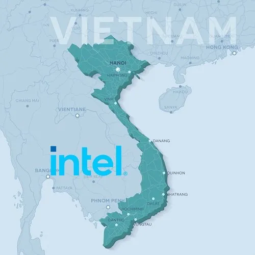
A 500,000 ft2 (~47,000 m2) state-of-the-art cleanroom facility still towers as the largest U.S. high-technology investment in Vietnam 10 years after starting operations in Saigon High Tech Park in District 9, Ho Chi Minh City. The structure built by Intel Products Vietnam (IPV) on the back of a $1 billion investment is the largest assembly and test manufacturing facility (ATM) in the Intel assembly and test network. IPV turns out products that are helping power cutting-edge applications along with the next wave of semiconductor industry growth as it homes in on 5G, Internet of Things (IoT), desktop and mobile. And it has been a boon to the local economy, generating more than 5,000 high-skill jobs across a number of assembly and test disciplines since launching operations in 2010. It has also contributed to over US$37 billion in exports from 2010 to 2019, accounting for over 60% of Saigon High-Tech Park’s annual export values in 2019. With its vision “to create the future of Intel and Vietnam,” Intel continues to be a strong long-term partner in Vietnam. I recently spoke with Kim Huat (KH) Ooi, vice president of Manufacturing and Operations and General Manager at Intel Products Vietnam (IPV), about the facility’s vital role in Intel’s overall manufacturing operations, its support for the E E ecosystem in Ho Chi Minh City, and measures it has implemented to reduce the impact of the COVID-19 pandemic on the facility and protect employees. Ooi leads and manages the site to support Intel’s business in Vietnam. His responsibilities include overseeing factory operations and employee relations; enriching the Intel image and brand; building strategic relationships with communities, media, governments, and local authorities; and working with the industry ecosystem and government. IPV employees celebrate Intel’s 50th anniversary in 2018. Ng: How does IPV campus complement the rest of Intel manufacturing sites and be nearer your customers and supplier base?Ooi: Intel Vietnam is an important part of Intel’s manufacturing presence worldwide. IPV has been operating for nearly 14 years in Vietnam and has celebrated multiple milestones along the way. As a site, we have matured and grown over the years. In March this year, we celebrated a proud milestone – the rollout our 2 billionth unit – that reflects the value of IPV to Intel Corporation as these Made in Vietnam products support its customers worldwide. One of our philosophies is to work with and grow local ecosystems in countries where we operate. In Vietnam, Intel has been offering technical and managerial expertise to many local suppliers in Vietnam to help them expand their business and services to other foreign direct investment (FDI) customers in the industry. Over the past 10 years, Intel’s supplier list has grown 10-fold from 20 in 2010 to about 180 suppliers in 2020.In today’s world of fast-changing consumer preferences and expectations, we need to help drive development of the latest products and technologies to support strong customer demand and new product portfolios such as 5G. To support evolving customer requirements, our workforce frequently upgrades its skills to work on new products and technologies.Intel as a company is also evolving as it transforms from a PC-centric to a data-centric organization, a shift behind the more than US$70 billion in record revenue Intel posted in 2019. Intel’s data-centric business accounted for more than half of that revenue. IPV plays a key role in Intel’s expansion into new market segments.Ng: What are the key differentiating elements (talent, tax, technology, trade, EHS) in Vietnam that have been instrumental in supporting the E E ecosystem in Ho Chi Minh City?Ooi: Vietnam’s stable political environment and increasingly liberalized trade and investment policies are great for businesses. The region’s young, talented workforce is also one of many competitive advantages that enables it to attract foreign investment. Intel’s announcement to invest in Vietnam in 2006 has played a large part in helping put Vietnam on the map of the global IT and semiconductor industry. The news helped attract industry suppliers and service providers, bolstering Vietnam’s economy and creating jobs. The Vietnam government also figured prominently in sparking the boon by establishing the right policies and incentives to attract foreign investment. Since starting operations, we have seen significant improvements in infrastructure such as roads, ports, airports, broadband and power supply. Vietnam’s standing in the global business community is even stronger today after the government successfully combatted the COVID-19 pandemic early on and introduced policies to help businesses restart operations. We expect all these factors to continue to make Vietnam an attractive relocation target for companies around the world. Ho Chi Minh City People’s Committee Vice Chairman Mr. Duong Anh Duc (center) visited Intel Vietnam to tour the state-of-the-art facility. Ng: What measures have you implemented to reduce the impact of the COVID-19 pandemic and protect employees? Ooi: COVID-19 has taken the world by storm and changed the way we work and live in many ways. It has unquestionably pushed the world to build stronger partnerships among individuals, organizations, businesses and communities. Intel’s manufacturing operations have continued to run at full capacity. Since the outbreak emerged, we have strictly followed required Intel safety measures as well as the Vietnam’s health guidelines. We have also implemented a number of other safety initiatives and protocols to ensure our business runs smoothly. We’re doing everything possible to ensure the well-being of our employees and help them better respond to the pandemic.In coordination with our strategic partners, we have been donating thousands of Personal Protective Equipment (PPE) to the Fatherland Front and Department of Health (DoH) since early March. Recently, in partnership with AmCham Vietnam, Intel donated an imported ambulance with built-in essential equipment to the Ho Chi Minh City 115 Emergency Center. Intel has also teamed with Saigon Hi-Tech Park management to donate two ventilators and N95 masks to DoH.Our employees are also helping out by donating to Vietnam’s Coronavirus Donation Matching campaign. We collected US$13,000 from Intel employees and included matching funds from Intel Foundation to support three non-profit organizations (NPOs) – Saigon Children’s Charity, Kidspire Vietnam and Teach for Vietnam. All told, Intel Products Vietnam has donated US$200,000 to COVID-19 relief efforts, demonstrating our long-term commitment to communities where we operate. Intel Products Vietnam teamed with AmCham Vietnam to donate a fully equipped ambulance to Ho Chi Minh City’s 115 Emergency Center, demonstrating IPV’s long-term corporate social responsibility commitment. In early May, Intel unveiled our 2030 Corporate Strategy and goals to accelerate progress against the world’s critical challenges and help drive positive global outcomes. Part of our 2030 goals, our RISE (Responsible, Inclusive, Sustainable, Enabling) strategy focuses on the company’s commitment to its corporate social responsibility (CSR) initiatives to create a more responsible, inclusive, safe and sustainable world through technology and collective action. IPV has also committed to implementing the RISE strategy in Vietnam with local community initiatives and technology interventions. Bee Bee Ng is president of SEMI Southeast Asia.
Read More
Tracking and quickly diagnosing COVID-19 infections, working from home and telemedicine recently came into sharp focus as technology executives and other subject matter experts from microelectronics heavyweights recently gathered for the first-ever virtual SEMI CTO Forum to explore how the microelectronics industry and their own companies can leverage future technology trends to drive growth. Themed Intelligent Medtech and Wearable Technologies, the forum drew CTOs from ARM, Babblelabs, Brewer Science, Dell, Dow/Dupont, E-Ink, Hewlett Packard Enterprise, Intel, Lam Research, KLA, Microchip, ON Semiconductor, Qualcomm, Tokyo Electron, Ulvac, Veeco and Xilinx. The event is designed as a strategic driver of pre-competitive innovation. Following are key takeaways from the forum. Microfluidics Promises to Speed COVID-19 Diagnosis More than 240 companies worldwide are developing microfluidics solutions to improve diagnosis and treatment of COVID-19 and other conditions, said forum speaker Dr. Kurt Petersen, a member of Band of Angels, Silicon Valley's oldest angel investment group, with an illustrious background1 in technology. And their innovations are bearing fruit. Cepheid, a company founded by Dr. Petersen, has developed a disposable microfluidic cartridge, Xpert Xpress SARS-CoV-2, used by doctors to swab the inside of a patient’s mouth. Highlighting the vital role of MEMS in medical electronics, the tiny powerful devices are behind a test that can detect COVID-19 infection in under 40 minutes. Dr. Petersen also cited a few examples of implantables and injectables under development, including: In vivo chemical sensing: Profusa developed a continuous glucose monitoring sensor via an optical patch. Glaucoma pressure monitors: Injectsense built a silicon chip the size of a grain of rice that is embedded in the eye to measure eye pressure. Retinal implants: Second Sight implanted a 60-electrode array chip that projects images onto the retina to improve vision. Microelectronics Takes Aim at Battling COVID-19 The event’s CTO roundtable, a platform for discussing societal and technology issues, revealed microelectronics technology will likely give rise to solutions for combatting pandemics and new business opportunities both in the short and long run. Areas of the greatest interest included: Tracking and Security: Infection tracking accuracy is key to limiting the spread of viruses yet comes with inherent privacy and security challenges. The consensus view of the executives was that developing trusted hardware capabilities is critical for adoption of accurate infection-tracking technologies. Remote Operation: Executives expect working from home or the use of telehealth to continue building momentum long after pandemic. To give staying power to the remote communications at the heart of these trends, microelectronics ecosystems will need to boost compute performance, both at the edge and in the cloud, while increasing bandwidth to enable applications such as augmented reality/virtual reality (AR/VR), artificial intelligence (AI), machine learning and advanced data analytics. Edge intelligence: The challenge of remote communications spans both people and the Internet of Things (IoT). Questions persist about how hundreds of billions of sensors will connect to the cloud and how much power they will consume. The need to push computing to where data is generated – at the edge – is rising and the necessary underlying technologies will only come by combining various forms of distributed computing and analytics. The microelectronics industry’s ability to seize these opportunities will only be possible with huge strides in innovation, raising concerns among the CTOs about the financial viability of cutting-edge devices because of increasing device complexity and R D costs. Technology partnerships and collaborations – an area where SEMI is contributing and will continue to expand its efforts as it works with the CTO community – will be critical to containing R D costs. SEMI will help the executives identify and mobilize the resources key to future innovation. Improving Home, Work Productivity and Experiences Key to AR Adoption Smart wearables also offer great promise. In just over a decade, AR and VR have grown from science fiction to practical uses such as AR applications for smart contact lenses, said Dr. Mike Wiemer, Co-Founder and CTO of Mojo Vision2. Dr. Wiemer said that while many AR applications remain under development, the technology will only see widespread adoption once it starts to improve productivity and efficiency at home and work and the quality of other experiences. The smart augmented reality contact lens developed by Mojo Vision is a step in that direction. The product’s built-in display gives users timely information about everything they see while remaining invisible by packing 70,000 pixels into a space smaller than a half a millimeter across, making it the smallest and densest dynamic display ever made. The contact lens is powered by an ARM-based processor, with later versions adding an image sensor, eye-tracking sensors and a communications chip. SEMI thanks EMD Performance Materials and Telit for sponsoring the CTO Forum. For more information on the CTO Forum and SEMI’s Smart Data-AI initiative, please sign up on our webpage. 1 Dr. Kurt Petersen is a member of the National Academy of Engineering, an IEEE Medal of Honor winner, and a Life Fellow of the IEEE for his contributions to the commercialization of MEMS technology. 2 Dr. Wiemer also co-founded Solar Junction, where he led technical teams to two world records in solar cell efficiency (43.5% and 44%). He also has patents and papers in Semiconductor Devices Applications, Silicon Photonics, Materials Integration, Lasers, Solar Cells, Solar Systems, and Analog Circuits. Tom Salmon is Vice President of Collaborative Technology Platforms at SEMI. Pushkar P. Apte, Ph.D., is Strategic Technology Advisor for the Smart Data AI Initiative at SEMI.
Read More
Humanity has survived almost unimaginable challenges over the past 5,000 years of documented human history. From war, famine and natural disasters to the first global pandemic in the last 100 years, more often than not, people have relied on one another to survive and thrive again. As the industry association representing the global microelectronics industry, SEMI has similarly made collaboration and community integral to the fabric of its organization. From helping members to succeed through the COVID-19 pandemic to facilitating member-driven industry standards around environmental health and safety, materials, and manufacturing capabilities, this approach shows members that standing together is better than standing alone.On the eve of the 50th annual SEMICON West (July 20-23, 2020) — the first virtual edition in SEMI’s history — I spoke with SEMI’s vice president of technology communities, Michael Ciesinski, about the role of SEMI in tackling big challenges through an active member community intent on solving problems through collaboration.SEMI: How long have you worked with SEMI and in what capacity?Ciesinski: In January 2016, I started my second tour at SEMI when FlexTech, the industry consortium I’d been leading, became SEMI’s first strategic partner. Nearly two years into that role, SEMI President CEO Ajit Manocha asked me to form Technology Communities to engage members with common interests. After FlexTech, we brought on the Fab Owners Alliance, then MEMS Sensors Industry Group (MSIG), and later the Electronic System Design Alliance (ESD Alliance).SEMI now has more than 20 communities in all, including Smart MedTech, Smart Data AI, Smart Manufacturing, Electronic Materials, and Integrated Packaging, Assembly and Test.SEMI: What is your role with Technology Communities — and how do members stand to benefit?Ciesinski: The leadership of Technology Communities ensures that SEMI’s benefits and services align to our members’ interests so we can provide member benefits that matter most. This spans forming communities where people hold common interests (e.g., advanced packaging) to facilitating standards that will promote intelligence in manufacturing (e.g., data standards for AI and machine learning) as well as providing R D funding.I’m especially proud that over the past three years, SEMI has brought more than $40 million in R D funding to our members, with most grants in the $500,000-$1 million range. We’ve been especially successful in securing funding in flexible hybrid electronics (FHE) through U.S. Army Research Laboratories (ARL), a model we first developed through FlexTech.Two recent recipients of FHE funding, GE Research and ITN Energy Systems, show how the grants are spawning partnership opportunities among commercial enterprises, R D organizations and universities. In developing lightweight, non-invasive wearables, including a human-performance sweat-monitoring patch that remotely analyzes sweat to detect hydration levels and other vital signs, GE Research is using key components such as sensors and lightweight batteries in its designs.ITN Energy Systems designed a flexible all-solid-state lithium battery that’s printed on light, flexible substrates to power small and incredibly thin applications.Universities are also benefiting by plugging into the SEMI ecosystem. In fact, 40-50 percent of funded projects are seeding commercialization by universities. This is another validation that SEMI’s collaborative, community approach to microelectronics is working.SEMI: Position, Timing and Navigation (PNT) is another hot area where SEMI has secured ARL funding. What makes this funding different and why is it important?Ciesinski: The PNT grant makes ARL funding available to the MEMS Sensors Industry Group (MSIG) members through SEMI for the first time. If you’ve ever lost GPS signal while coming out of a tunnel, you know how frustrating that is. For us, that’s an inconvenience, but for a healthcare worker in a remote location who’s waiting for a delivery of medication by drone, it could be life-critical. While that’s just one example of why we need PNT to operate when GPS isn’t available, I can imagine dozens of other important dual-use cases, including autonomous driving.SEMI: How else do Technology Communities benefit under SEMI?Ciesinski: Technology Communities need access to diverse resources to spur continuous innovation. Electronic Materials Group participants, for example, need to stay informed on regulations coming out of Asia, the U.S. and Europe that may affect their businesses. Where else other than SEMI can like-minded stakeholders congregate with people up and down the supply chain to determine whether industry-wide action is needed on regulation?SEMI: What is the importance of SEMI’s global footprint?Ciesinski: I’ve worked with many associations and managed major industry consortia. The clear advantage of SEMI is our global footprint. And that’s vital because microelectronics is a global industry involving a multitude of stakeholders that play essential roles in the supply chain.Let’s say you want to discuss EU regulations on hazardous chemicals. Rather than decipher these complexities alone, you can pick up the phone to speak with someone on SEMI’s European team to learn what’s critical.What if you’d like more information on the 20-plus new fabs that are going up in China? You can explore that question with our SEMI China or SEMI Industry Research and Statistics teams.SEMI: How has SEMI evolved over the years?Ciesinski: SEMI has a long history of providing what the industry cares about. We started in trade shows and pivoted to industry standards. We began with small silicon wafers and wafer carriers, and now within the span of 50 years we’re working on data-format standards that will support the application of AI and machine learning (ML) in the semiconductor industry.While highly varied today, data-format standards will help component manufacturers refine processes to create more efficient solutions. This ARL-funded program, which pairs SEMI members with the grant recipient, Cornell University, may offer dramatic gains in the productivity of semiconductor manufacturing.SEMI: How does SEMI’s approach to COVID-19 reflect core values of collaboration and community?Ciesinski: Together with Ajit Manocha, CMO Terry Tsao and other team members at SEMI, we pulled together a task force to help SEMI members navigate the pandemic.We tapped two existing groups, Environment, Health and Safety (EHS) and Information Technology Leadership (ITL) from the start, documenting their strategic and tactical approaches to help all members through the COVID-19 resource section of our website. The EHS section provides tips on facilities and meetings, employee policies, business travel and communications, while the ITL section lists insights on computing hardware for staff, licensing, networks, security and employee policies.Our EHS leadership team, which includes Entegris, Axcelis, Versum, and Intel, immediately started sharing best practices for sanitizing facilities. As a result of team meetings, SEMI EHS shared best practices on keeping the workforce remote and guidelines for returning people to work safely. From securing PPE and safeguarding employees and visitors by performing thermal scanning to outlining communications around potential employee exposures, EHS has provided meaningful resources for the benefit of all members.SEMI also took immediate steps in the area of advocacy. Our advocacy team in Washington, D.C., together with regional SEMI presidents around the world, have ensured that semiconductor facilities were and still are considered essential businesses in the U.S., Europe and Asia. That’s because microelectronics are foundational to fighting the pandemic.Microfluidics are critical to the Reverse Transcription (RT) Polymerase Chain Reaction (PCR) tests most commonly used for COVID-19. Sensors are embedded in the pulse oximeters that allow patients and healthcare professionals to monitor a vital rubric: oxygen saturation level. If oxygen saturation level drops into the low 90 percentiles or below, it may be time to go to the hospital for treatment.Microcontroller units are essential components in a wide range of hospital equipment, including the ventilators that may make the difference between life and death in the most seriously ill patients.SEMI: How can the ingenuity realized through microelectronics continue to help us tackle other big problems? Ciesinski: We have MEMS and sensors to thank for distributed intelligence, giving us the ability to put sensors anywhere, locally based in the field or in the packaging house.Food production is a prime example. Leveraging miniaturized wirelessly connected sensors, we can trace food through the entire production lifecycle, from the seed in the ground to the food in the warehouse and, ultimately, to the product that lands on the table.From larger enterprise such as IBM Food Trust to small startups, we’re using MEMS and sensors to improve crop yields so we can feed a human population that’s growing each year.There’s a sustainability piece as well. We’re using MEMS and sensors to reduce the amount of fertilizer or other nutrients or chemicals in the soil. That’s good for the environment and for the agricultural workers who labor in the fields.MEMS and sensors can also condense the time it takes to perform a specific task, conserving human resources.SEMI: Where do you think SEMI will go in the next decade?Ciesinski: Ten years from now, I believe we will still have our global footprint in place. I expect it will expand, particularly in Asia.We may also expand into new areas such as Latin America and Central America, which would provide at least two major benefits: People working in microelectronics would, I hope, have access to better quality of life. And diversifying the supply chain would allow nations and regions to have more control over the products they need, from PPE to medications, which may help us to better manage through the next pandemic.I am also hopeful that SEMI will be on the leading edge of helping our members communicate in much different fashion from what we have today. We’re already expanding beyond the paradigm of in-person meetings for standards meetings and conferences. As we move forward, I think we’ll see a hybrid solution to doing business, combining in-person meetings with virtual conferences and digital content that’s available 24/7.Whatever changes we see in SEMI, I’m confident that we will continue to see a global footprint in an industry association that prioritizes connections among members.Engage in the SEMI experience at upcoming SEMICON WestRegister today to hear from keynote speakers such as environmental advocate and former U.S. Vice President Al Gore, futurist and author Steve Brown, and IBM Research senior vice president and director Dr. John E. Kelly III, and Lea Gabrielle, special envoy of the Global Engagement Center for the U.S. State Department, at SEMICON West , July 20-23, 2020. Content will be live streamed and available on-demand. Michael Ciesinski is vice president of Technology Communities for SEMI, the global microelectronics industry association, appointed in August 2018. At SEMI, he directs activity for more than 20 industry groups, oversees the association’s R D funding program, and develops new technology initiatives to serve SEMI’s 2,400 members. Prior to re-joining SEMI, Ciesinski was president/CEO of FlexTech Alliance, an industry consortium focused on new methods of creating electronics. From 1995-2008, Ciesinski served in a similar role at the U.S. Display Consortium (USDC), a private/public partnership chartered with building the infrastructure for electronic display and flexible electronics manufacturing. Both FlexTech and USDC annually sponsor multimillion dollar technology development programs and provide industry technical, financial and market services. Ciesinski is a graduate of the University of Albany, NY, and a former member of the Dean’s Advisory Committee at California Polytechnic State University.Maria Vetrano is a PR consultant at SEMI.
Read More