downloadGroupGroupnoun_press release_995423_000000 copyGroupnoun_Feed_96767_000000Group 19noun_pictures_1817522_000000Member company iconResource item iconStore item iconGroup 19Group 19noun_Photo_2085192_000000 Copynoun_presentation_2096081_000000Group 19Group Copy 7noun_webinar_692730_000000Path
Skip to main content
Default Banner Image

Singapore

Nexperia became a standalone company about four years ago after our divestiture from NXP Semiconductors. Last year we started our journey towards smart manufacturing at our back-end factories in Asia by developing a roadmap to help steer us in the right direction.Our first step to creating a convincing and workable smart manufacturing roadmap was to define the very meaning of smart manufacturing to Nexperia. Since the definition of smart manufacturing varies widely, we started by looking at two different and distinct technology adaptations: Physical automation Data-driven manufacturing, or using analytics at the core to develop and adopt machine learning and artificial intelligence (AI) models It is important to find the right balance of investments between physical automation and data-driven manufacturing to steer clear of deployment inefficiencies since only connected solutions deliver full value. Our approach involved the following high-level steps. Meeting with internal management teams for their inputs and examining factory needs and maturity Meeting with other semiconductor factory operators, subcontractors and partners to review their smart manufacturing approaches and challenges Evaluating our needs and status against the Singapore Smart Industry Readiness Index model Physical AutomationEvaluating the maturity of available solutions and adaptions by the industry and our own shop floor helped simplify the thought process quite well. Logistic automation is not new. Very mature solutions, even for custom layouts and preferences, are readily available. Shop floor automation is far more difficult than logistic automation since variability is simply too high. Traditional shop floor investments were always driven from quality or OEE perspectives and not necessarily very well connected. Our approach is outside-in – deploy logistic automation first and then move to the shop floor.Data-Driven ManufacturingHow smart manufacturing becomes depends on the extent to which a factory is data-driven. Enabling data-driven manufacturing requires foundational investments to improve traceability, connectivity and real-time operations. We believe real-time awareness can drive machine-level and closed-loop process control critical for predictive, cognitive control of the shop floor.Real-Time Awareness and Traceability is at the CoreDeveloping real-time awareness requires wide-ranging manufacturing protocols. The following focus areas have helped us simplify the challenge: Connectivity Core systems for areas including MES, quality and SAP Analytics and AI Digital shop floor featuring one operator interface with real-time control systems Readiness of engineers, technicians and managers Each of these pillars has different level of complexity due to legacy equipment and systems, legacy processes and inexperience of engineers with automation. This makes deployment of data-driven operations a complex challenge. We looked at different project approaches for each of the focus areas: Core Systems – Build additional technology enablers and roll them out with prioritization planning. Analytics – Focus mainly on OEE and yield with automated root cause analysis and predictive approaches. Real-Time Control – Merge the initiative with factory-level programs to improve productivity and quality. With a strong smart manufacturing roadmap, the next challenge is to secure long-term buy-in on the plan and required investments from executive management. Visiting and otherwise connecting with peer sites that have already deployed smart manufacturing infrastructure is vital in this effort. Thanks to SEMI members, we were allowed to visit their factories with our management team for go-and-see tours since seeing is believing in the smart manufacturing journey. Our executives also met with subcontractors and vendors to better understand the value of this transformational undertaking.A long-term outlook is necessary to successfully develop a smart manufacturing roadmap, and executive commitment goes a long way to ensuring its success. We are excited about our smart manufacturing journey and believe it is a game changer for our factories.Adarsha MARPALLI is director of Factory Automation at Nexperia B.V.
Read More
D-SIMLAB Technologies, a Singapore-based provider of simulation-based business analytics and optimisation software solutions, recently joined SEMI. I spoke with Peter Lendermann, the company’s co-founder and Chief Business Development Officer, about the company’s role in the smart manufacturing movement, how customers are benefiting from D-SIMLAB solutions, and what the future holds for smart manufacturing. Ng: What is D-SIMLAB’s mission?Lendermann: Our mission is to develop, market, and deliver high-performance simulation-based decision support solutions that enable corporations to enhance their performance in a sustainable manner leading to significant cost savings. In particular, we focus on semiconductor manufacturing material flow planning and optimisation but also do business in aviation where we help customers optimise their spare parts support operations. What these two domains have in common are three important attributes: They are capital intensive, their underlying operations are complex, and operations are also heavily affected by random, i.e. unpredictable events, which makes both planning and execution of manufacturing operations very challenging. D-SIMLAB is a spin-off from the Singapore Institute of Manufacturing Technology (SIMTech) under the Agency for Science Technology and Research (A*STAR). Our head office is in Silicon Island Singapore. We also have representations in Germany and the U.S. Most of our staff are industrial and computer engineers with up to 20 years of operations experience in their respective industry domain, as well as vast data analytics and software development capability.Ng: What solutions does D-SIMLAB offer to optimise semiconductor manufacturing?Lendermann: In the three-pillar smart manufacturing framework of Connect, Sense and Predict advocated by SEMI, our focus is on Predict though we emphasise the equal importance of the subsequent Act: Our solutions can Predict, for example, WIP waves or usage-based preventive maintenance due dates. But much more value-add can be realised once some decisions with regard to how to Act can be derived from such a prediction. The ability to pro-actively adjust action plans in a timely manner is essential to overcoming challenges arising from changing customer due dates, mix profile changes, untimely production line issues, and production capacity to be shared with R D lots effectively, so that ultimately our customers can enhance capacity, reduce cycle times and improve the due-date performance of their factories.To that end, our D-SIMCON solution suite spans the full spectrum of decision-support tools required to forecast, manage and optimise material flow – from operational scheduling and dispatching, WIP forecasting and dynamic and static capacity planning all the way to specific applications for fab load mix optimisation or for the enhancement of the product/layer dedication and resist allocation in the lithography area. Our solutions are implemented in numerous 6-, 8- and 12-inch wafer fabs operated by both IDMs and foundries worldwide with capacity ranging from 40,000 to 200,000 wafers per month.Ng: What are the key enablers of D-SIMLAB’s success?Lendermann: Our success lies in deploying production-ready solutions for our customers, allowing them to extract immediate value. Our solutions enable the portrayal of many domain-specific characteristics such as queue time constraints or specific equipment behaviour, which is absolutely essential to generating operationally feasible plans or schedules in order to be able to Act in the best possible manner according to what has been Predicted. Moreover, we have modules for automatic generation, calibration and maintenance of the underlying capacity model, including resolution of data inconsistencies as well as verification and validation of the model, to allow near real-time responses to continuously changing operations. And the associated optimisation approaches focus on creating maximum possible value with as few iterations as possible and within minimum time through smart heuristics and parallel computing infrastructure – a paradigm that is as powerful as it is cost-effective.Ng: What are a few of your more notable customer successes?Lendermann: As a result of the first implementation of our novel, multi-objective based Scheduler cum Dispatcher, a tool capacity gain of 8%, a transportation capacity gain of 10%, and an operator workload reduction of 25% were concurrently realised at one of the critical equipment groups in our customer’s fab. At another set of equipment groups in the same fab, a 7% increase of lots within the critical queue time limiting area was achieved.Another use case we successfully realised is fine-tuning of Preventive Maintenance plans: Based on a seven-day lot arrival forecast at each equipment generated with our WIP Forecaster, a recommendation is made when PM would be best possible without causing too much disruption in the WIP flow. The effect of this synchronisation of the PM plan with material flow enabled a dramatic reduction of the average queue lengths at critical equipment groups and the associated cycle times without incurring any capacity loss. Reduction of average queue length as a result of synchronising preventive maintenance with material flow. Ng: What challenges has D-SIMLAB been facing in the COVID-19 world?Lendermann: Obviously, software delivery projects have become more challenging for the time being since our engineers cannot be on-site frequently. But it also turned out that more and more services can be delivered remotely, which has the nice side effect of making the services more cost-effective for customers. Overall, we are confident that our solid customer base will enable us to sail steadily through these challenging times.Ng: Where does D-SIMLAB see the technological development heading?Lendermann: In the future, enriching decision support and manufacturing execution solutions with machine learning and other AI techniques will be critical in reducing dependency on human experience. This path is essential to making manufacturing operations fully Industry 4.0-compliant. D-SIMLAB will certainly be at the forefront of this development. Bee Bee Ng is president of SEMI Southeast Asia.
Read More
Not long after STMicroelectronics opened its first semiconductor plant in Singapore more than 50 years ago, a facility chiefly focused on chip assembly and packaging, the company realized that it had constructed the site in an area with a blossoming chip ecosystem with a bright future. Before long, the company became the first to start a wafer fab facility in the so-called Little Red Dot. Today, our STMicroelectronics Singapore campus sports several buildings that dwarf the original site in the sprawling Ang Mo Kio Industrial Park 2. The facilities feature advanced 200mm manufacturing lines but still produce huge volumes of chips with more than 1,000 pieces of 150mm manufacturing equipment.Much of the wafer equipment dates back to the past century so is no longer supported by the manufacturers, if they’re still even in existence. Yet decades later the chipmaking gear continues to operate with a surprising reliability that far surpasses the longevity called for in its manufacturing specifications thanks to replacement parts and frequent upgrades with more sophisticated handling robots and chucks. Now, as smart manufacturing begins to establish a foothold in the semiconductor industry, Industry 4.0 technology is breathing new life into these aging workhorses.Despite its age, all of the equipment adheres to industry manufacturing standards. The gear is remotely controlled using the SECS/GEM interface protocol that was either originally integrated with the equipment controller or custom-made. We’ve also maximized its usage through advanced recipe management, advanced alarm and event handling, and secured lot identification.Crucially, we decided to systematically deploy a real-time fault detection and classification (FDC) solution using a third-party product based on what today is known as an edge computing architecture. Every piece of critical processing equipment is progressively paired with its dedicated FDC instance running on a virtual machine in the wafer fab data center, and the FDC solution monitors vital equipment parameters at high frequency – depending on the SECS/GEM capabilities of the equipment – and analyzes incoming manufacturing data in real time using classic SPC (statistical process control) algorithms and even AI-class protocols.Our use of the FDC edge solution as a sensor signal aggregator has given our equipment a second life. The solution processes real-time signals from sensors connected through a typical TCP-IP. Sensors have been the old equipment’s saving grace with their ability to de-multiply equipment capabilities and overcome fundamental shortcomings and design weaknesses. The STMicroelectronics Singapore plant first used off-the-shelf sensor nodes with built-in power amplifier and analog input nodes. While very practical and easy to implement, deploying the nodes can be costly. After developing more expertise in sensor integration using FDC, our wafer fab equipment experts decided to design an in-house solution based on the famed STM32 microcontroller. Leveraging Arduino – an open-source electronics platform with easy-to-use hardware and software – the equipment teams can now design and program a variety of in-house sensors for measurements including temperature, humidity, waterflow and pressure. The sensors are integrated with process equipment using the FDC solution. Integrating the sensors with the FDC engine on the edge computer extends the capabilities of old equipment without jeopardizing the integrity of the machines themselves. While the integration can be quick, it must be robust to ensure the reliability of the new measurements. Similarly, ever-increasing connectivity requirements present clear cybersecurity risks that must be managed upfront and each solution must be hardened to minimize security vulnerabilities. Even so, the challenges and risks pale in comparison to the benefits! Jean-Marc PHILIPPE is DIT Director at STMicroelectronics Pte Ltd. He oversees the deployment and support of Digital Solutions to enable STMicroelectronics front-end operations in Singapore and manages manufacturing productivity and automation programs at site level.
Read More
SEMI is pleased to welcome Singapore-based UTAC Holdings Ltd., formed nearly 50 years ago, as a new member. UTAC is a leading independent provider of assembly and test services for a broad range of semiconductor chips, offering a full range of semiconductor assembly and test services across analog, mixed-signal and logic, and memory. Its customers are primarily fabless companies, integrated device manufacturers and wafer foundries. The company has production facilities in Singapore, Thailand, China, Indonesia and Malaysia as well as sales offices in five regions: the United States, Japan, China, Taiwan, the rest of Asia and Europe.I recently spoke with Dr. Nathapong Suthiwongsunthorn, Vice President and General Manager of UTAC Thailand, about UTAC’s smart manufacturing advances, the company’s role in the semiconductor industry’s transformation, and the industry outlook for Thailand over the next year.Ng: How does UTAC Thailand complement your other facilities?Dr. Nathapong: As one of the world’s largest producers of quad-flat-no-leads (QFN), UTAC Thailand has significant capability in assembly and test of advanced leadframe products including power products such as Cu Clip packages as well as MEMS products. We also serve top global IDMs and have the largest share of assembly and test for the automotive market among all UTAC operations. UTAC’s other facilities have expertise in wafer-level packages and system-in-a-package and serves the communication and consumer market not only for IDMs but also for the fabless and foundry companies. The Thailand factory nicely complements the other UTAC facilities both from the standpoint of operational and marketing diversity. Ng: UTAC Holdings Ltd. announced in August this year that it has completed its sale to Wise Road Capital, a global private equity firm. Will this in any way change the operation and business strategy of UTAC Thailand?Dr. Nathapong: I don’t believe it will change the way we operate. However, the acquisition is very positive for us from a financial perspective. With the benefit of significantly reduced debt and interest expenses, we will be able to expand our business to grow with and hopefully beyond the semiconductor market. Ng: To what extent has UTAC adopted smart manufacturing?Dr. Nathapong: UTAC Thailand is leading the way in terms of automation, smart manufacturing and Industry 4.0 with our in-house automation team and unique expertise. For example, we have built our own inspection equipment that is much faster and cheaper than what is commercially available. We also working on many programs such as mobile robot, AGV, auto inspection and office automation to help drive greater production efficiency. We are replicating our manufacturing advances and fanning them out to other UTAC facilities.UTAC Thailand Ng: What are some of the challenges you face in pushing for the industrial transformation in Thailand?Dr. Nathapong: I think the key challenge is to find skilled engineers who can perform hardware- and software-related tasks critical to the industrial transformation. But frankly, we have done a good job in managing this challenge by hiring very smart people, providing them with the required in-house training, and using outside training for new recruits as necessary. We have developed partnerships with capable vendors in this regard as well.Ng: What are the key differentiating elements (e.g. talent, tax, technology, trade, EHS) in Thailand that have been instrumental in supporting the E E ecosystem?Dr. Nathapong: There are two key differentiating elements for us. Firstly, UTAC has been around for over 47 years and is very well-established in Thailand with a positive reputation as an employer. This makes hiring talented people relatively easy. Secondly, and perhaps more importantly, the nature of the Thai people and also the benefits the company provides make it relatively painless to retain key employees. I also believe that we have a significant number of engineers available in Thailand. Finally, labour costs in Thailand are still very reasonable and stable. So we are able to acquire talent at a very competitive rate compared to other countries. Ng: What is the industry outlook for E E industry in Thailand over the next year?Dr. Nathapong: Surprisingly, the current sad predicament of COVID-19 has shown no negative impact for the global semiconductor industry – people seem to be buying more electronics with the lockdown. Our outlook for the Thailand’s E E industry is similarly very positive. Most semiconductor companies including UTAC see significant growth this year and I hope it will continue.Ng: With the recent semiconductor geopolitical and trade tensions, are more customers moving their business to Thailand?Dr. Nathapong: I believe so. We do see some of our key customers move manufacturing out of China and into Thailand. The relocations help them offset or avoid any potential fallout from current geopolitical tensions.Ng: In what areas do you think SEMI Southeast Asia can play a role to help our members companies in Thailand like UTAC?Dr. Nathapong: The semiconductor industry has been in Thailand for a long time. In fact, UTAC Thailand is 47 years old this year! However, I feel that Thailand never really worked with a strong establishment organization like SEMI that can connect various companies together to help drive innovation. I think SEMI Southeast Asia can truly help Thailand to move up to the next level of providing semiconductor solutions globally. We welcome SEMI Southeast Asia’s help in this regard.About Dr. Nathapong SuthiwongsunthornDr. Nathapong Suthiwongsunthorn joined UTAC in 2009 and is currently General Manager of UTAC Thailand, UTAC’s largest operation site. Before taking over the management of Thailand operations, he was Vice President of Research and Development, running UTAC’s global R D group. Dr. Nathapong has more than 20 years of experience in the semiconductor industry. He holds more than 40 international patents and publications in wafer-level and advanced packaging.Prior to joining UTAC, Dr. Nathapong held several key leadership positions in research and development at Schott, STATS ChipPAC and Infineon. Dr. Nathapong has a Ph.D. in Electronics Engineering from Oxford Brookes University, England.Bee Bee Ng is president of SEMI Southeast Asia.
Read More
I recently spoke with Chan Pin CHONG, Executive Vice President and General Manager of Products and Solutions at Kulicke Soffa, about how smart manufacturing is driving new production efficiencies in the semiconductor industry. During our conversation, he also provided practical steps for factory operators to follow in evaluating their smart manufacturing needs in order to ensure successful implementation and discussed the potential payoffs. Based in Singapore, Kulicke Soffa is a leading global provider of ball bonding, advanced packaging, wedge bonding, and electronic assembly equipment for the semiconductor, power and automotive industries.Ng: Industry 4.0 and smart manufacturing are critical to the growth of the semiconductor industry. What does the smart manufacturing movement mean to you or Kulicke Soffa?Chong: The future of smart manufacturing is the vision of building a digital connected factory to drive new manufacturing efficiencies by combining physical and cyber technologies. Industry 4.0 integrates discrete systems and harnesses the power of large volumes of data to move towards greater automation.At K S, we define smart manufacturing across the following four key areas embedded in our roadmap for all K S products, from wire bonders and advance placement tools to pick and place machines: Interoperability – This is about machines, devices and sensors connecting to each other. In fact, the very basis of smart manufacturing is that all devices are connected. Information transparency – Through simulation, various artificial intelligence (AI) tools use contextual information to emulate the actual world. Technical assistance – Robots or machines support humans in making decisions or solving problems. Autonomous decision-making – This is our vision that robots or machines can learn from machines to make decisions on their own. Ng: Please elaborate on some of these areas and how they’re the relevant to smart manufacturing. Chong: The need for machines, devices and people to communicate with each other forms the basis of connectivity, the idea of all machines communicating with each other or a host. Connectivity protocols now in place for machine-to-machine connectivity include SEMA, SECS/GEM, SEMI-ELS and IPC-CFX. Machine technology uses various sensing technologies. For example, for a pick and place machine such as SMT platform on K S Hybrid, the algorithm to recognize and align processes is part of the sensor needed in each machine before to can process and add thousands of components to the substrate or panel. In a wire bonder, the ultrasonics or EFO signal can provide some form of sensing technology for a machine to detect process conditions. Importantly, these sensing technologies can be used to collect feedback for process improvements.One example of how K S machines are connected to the host is our use of an intermediate server or host named KNeXt to connects to all assembly equipment in the fab. The equipment can then, in turn, connect to an external secured cloud or K S Global Cloud.Ng: What are the objectives for smart manufacturing?Chong: The ultimate goal is to achieve higher factory productivity or better OEE (Overall Equipment Effectiveness) by improving machine yields, productivity and efficiency. The key is to leverage AI, 5G, the Internet of Things (Iot) and other industry 4.0 technologies to drive automation and process improvements. Ultimately, each factory must meet productivity, yield and cost goals. Smart manufacturing enables factory operators to meet these goals. That is the focus of smart manufacturing.Ng: What is the biggest potential benefit of smart manufacturing?Chong: Smart manufacturing uses data to predict outcomes of a process step or machine operation. Once data is available in the global cloud, analytics can start to build data sets to run statistical modelling and examine factory operation trends. We can also use the data to identify past machine behaviors in order anticipate outcomes, including undesirable ones that we can then prevent.In the SMT example, if we can systematically examine days or weeks of historical performance, we can plot some statistical variations in the process specifically to a pick or placer or a robot and anticipate or avoid problems. However, all sensors must be in place in the bond head or the robot so that we can detect changes or variations in the robot’s movements.Kulicke Soffa smart manufacturing facility Ng: What are some recent factory improvements smart manufacturing has enabled? Chong: Kulicke Soffa has contributed to the hierarchical architecture of the smart factory and key technologies. COVID-19 is driving demand for greater factory connectivity, and K S offers solutions that are key to remote management and full control of smart equipment from a central control and embedding Internet of Things (IoT), big data, cloud computing and sensors in manufacturing. Using these technologies, a small smart factory can be remotely operated and managed.With COVID-19 limiting air travel around the world and access to support engineers, the need has grown for remote machine access to reduce the downtime per machine. Remote factory access enables off-site engineers to remotely identify and diagnose machine problems.Ng: What are barriers to faster adoption of smart factories?Chong: While most smart factories are capable of network connectivity and data collection, a key challenge is the lack of a business model for smart factories and smart equipment. Most factories must justify major capital investments by demonstrating ROI (Return of investments) potential. Capital improvements for every factory usually take several years to implement and are based on a complex business model. Factory connectivity requires substantial investments and years to implement. The same is true of the cloud infrastructure buildouts necessary to generate big data and meaningful analytics. The executive mandate for factory management to install capability usually calls for specific business targets in the planning stage.Another longstanding barrier to entry is the lack of compatibility of existing tools with new factory protocols, raising the question of whether the cost of replacing legacy tools justifies the need for a smart factory. If new factory investment is required for the latest tools to support the production of new products, the ROI will be much easier to justify.Ng: How is AI is important in smart manufacturing?Chong: AI interprets and learn from data to perform tasks and meet specific goals. Good examples of AI implementations include Amazon’s Siri and Alexa voice-command devices and self-driving cars being developed by Google and Tesla.At K S, over the years we’ve implemented AI in our smart wire bonders to reduce human intervention in our ProCu-7, PSP-2, ProCu Loop 2, Pro Bump and overhang processes.Thanks to AI, with senses of signals from the bonder, we can reduce the amount of parameters that an engineer or technician have to do trial and error. With on bonder metrology, PBI, loop height, wire sway features, AI allows us to measure process efficiency and provide feedback.Over several years of AI development, we have leveraged the technology to monitor machines and provide real-time performance feedback in order to provide better closed loop control such as short tail recovery in our bonder process. We can also use the data to predict machine behavior, monitor its health and track maintenance. Ultimately, AI enables fabs to improve manufacturing efficiency, productivity, yields and device quality.Ng: What’s an example of how AI has solved your manufacturing equipment problems?Chong: We’ve used AI to set RPM (real time monitor) limits, identify defective P-parts and monitor various conditions such as wire size and capillaries. These types of cases can arise in any manufacturing environment as humans make process mistakes or use the wrong part for a machine. With AI, we can prevent these problems and reduce the risk of further material lost from the wire bonding process.Ng: What advice do you have for factories looking to implement smart manufacturing systems?Chong: To build a smart factory, start by focusing on a clear set of business objectives and how smart manufacturing will help minimize or eliminate current factory inefficiencies. In other words, start with the end in mind – the problems that needs to be solved and the business goals – and identify the information you need to demonstrate ROI. Do you need to resolve, automate or improve processes or just to be more efficient? Before investing millions or billions of dollars to build a smart factory, identify those clear goals upfront. Then map out the particulars of implementation to avoid major problems around standards, protocols and connectivity.Bee Bee Ng is president of SEMI Southeast Asia.
Read More
Teck Khiong, WOI, senior manager of Factory Integration at Infineon Technologies Asia Pacific Pte Ltd, recently shared with me how the Infineon backend plant in Singapore has benefited from its journey to qualify for the lighthouse certification.WOI is driving Infinion smart manufacturing projects with a strong focus in the area of connect and control using IoT (Internet of Things) and analytics technologies. Ng: How did the Infineon backend plant in Singapore distinguish itself to qualify for lighthouse certification? WOI: The Infineon Singapore backend manufacturing plant is proud to be a Lighthouse Certified Smart Manufacturing site as part of the World Economic Forum’s (WEF) Fourth Industrial Revolution platform. Our Industry 4.0 (I4.0) implementation reduces labor costs by 30% and improves capital efficiency by 15%. We drove this successful digital transformation continuously investing in our people development and digital backbone.Of the many initiatives under our I4.0 Smart Factory platform, five were selected for WEF Lighthouse submission and certification. Digital foundation with integrated connectivity and workflow execution We implemented an Internet of Things (IoT) framework to connect machines to manufacturing system more than two years ago. The digitization of our Work-in-Progress (WIP) management systems provides full traceability and gives us better control of the four Ms (Man-Machine-Method-Material). Material handling and process automation We progressively deployed automated solutions starting six years ago using autonomous transport, robotic material management systems and automation of packing processes. This eliminated non-value touches in areas of WIP storage and retrieval. Advanced algorithms enabled WIP scheduling and dispatching As our product mix and volume grew in complexity, our advanced algorithms has enabled us to increase our machine uptime, thus reducing idle and set-up time. Manufacturing control tower Our control tower provides a real-time pulse of the entire manufacturing process, from machine efficiency to quality. The tower also improves data integrity and collaborative information sharing while issuing early-warning alerts that enable exception management and timely decisions. Running a global virtual factory Our Global Production Network deployments allows us to connect and manage a growing contract-manufacturing network in real time, with the same transparency, traceability and control as if the manufacturers are our internal sites.About Teck Khiong, WOITeck Khiong, WOI graduated from Loughborough University in the UK with a Master of Science degree in Computer Integrated Manufacturing (CIM). For more than 20 years he has delivered manufacturing IT solutions to global backend (assembly and test) semiconductor manufacturing, ranging from equipment, factory, process control, material handling automation and manufacturing execution systems (MES).
Read More
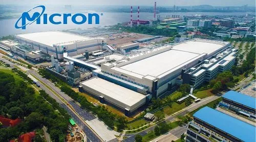
Making Strides TogetherKnowledge is power – especially when it is shared. This principle formed the foundation for Micron’s Go and See virtual visit of its Singapore manufacturing plant on 26 August 2020 as 27 companies including GLOBALFOUNDRIES, ST Microelectronics, Infineon, TEL, ViTrox , IBM, HP and UTAC joined the first-of-a-kind virtual factory visit. The chip industry powerhouses gathered to see how Micron’s Lighthouse frontend wafer fabrication facility leverages Fourth Industrial Revolution technologies to drive new production and cost efficiencies.They saw clear markers of a transformed organisation and spoke with working-level staff, managers and front-line employees. Company representatives also met virtually with Micron management teams from organisations that led its digital transformation – from pilot programs to integration at scale – to realise significant financial and operational benefits. The mix of technologies they deployed to make it all happen included artificial intelligence (AI), big data analytics and the Industrial Internet-of-Things (IIoT).Micron’s Singapore-based fab facility earned Lighthouse certification earlier this year from the World Economic Forum’s Global Lighthouse Network. The Go and See tour was co-sponsored by SEMI Southeast Asia and McKinsey Company.Transformation is CrucialBy embracing Lighthouse principles, semiconductor sectors and companies can accelerate their digital transformation to boost operational and financial efficiency while helping increase productivity across the electronics supply chain. It will take time for Southeast Asia semiconductor manufacturers to transform to digital operations, though we’re seeing growing interest in Industry 4.0 practices as they begin to understand that the deployment of new technologies and applications will help them better understand real-world benefits of smart manufacturing use cases and solutions. SEMI believes shining the spotlight on companies like Micron can illuminate the way forward for other companies to help drive the industry’s digital transformation. We look forward to seeing companies build on this momentum as they start to leverage leading-edge technologies to improve efficiencies and promote sustainability.Bee Bee Ng is president of SEMI Southeast Asia.

Read More
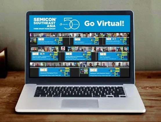
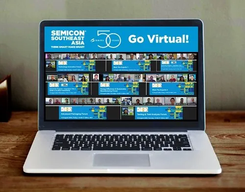
Never before had we expected that SEMICON SEA 2020 would go virtual.The COVID-19 crisis abruptly halted our ability to hold our premier Southeast Asia electronics manufacturing exposition as we typically do – in the physical realm. The pandemic tested our adaptability, challenged our willingness to experiment and, perhaps above all, accelerated not only our own but the world’s digital transformation. We had to change our way of doing business and learn to connect virtually like we had never had before. SEMI continues to believe that virtual interaction is no replacement for face-to-face engagement. But, like the rest of the world, we fast-tracked our digital education and staged the virtual event 20 July to 21 August 2020 to gather supply chain players and help fulfill the tremendous potential of our great industry. For all the suffering the COVID-19 has caused, the pandemic has underscored an important truth – that we need innovation through collaboration now more than ever to help solve the world’s greatest problems. We thank all our event sponsors as we turned what started as a grand experiment into a successful event that drew nearly 3,000 attendees to our webinars, business matching sessions and other online offerings designed to help them uncover new business opportunities. Following are other highlights. Southeast Asia Pavilion at Virtual SEMICON West 2020 In our first collaboration with SEMICON West, our Southeast Asia Pavilion at the event welcomed virtual visitors from around the globe to help them form new connections and grow their businesses. Business Matching Sessions Technical buyers from more than 15 multinational companies along with 141 pre-qualified suppliers attended more than 50 meetings across four online business matching sessions.Technical WebinarsCompany representatives from regions including Malaysia, Singapore, Vietnam, Taiwan, the United States, the UK, Israel, China and Japan shared their expertise and industry insights at SEMICON Southeast Asia 2020 webinars. In addition, experts from leading semiconductor companies such as Micron Semiconductor Asia Operations, ViTrox Corporation Berhad and A*STAR took part in our technical exchange by sharing the latest trends in the rapidly evolving semiconductor industry. Talent Development: Inspirational University Program Talks With building the talent pipeline critical to sustaining growth of Southeast Asia semiconductor manufacturing dynamics, talent champions from Lam Research and GLOBALFOUNDRIES highlighted career opportunities and pathways for young engineers while generating recruiting leads. More than 750 students from Malaysia and Singapore engaged panelists with questions during the sessions. The SEMICON Southeast Asia team extends its tremendous thanks to sponsors and attendees for their support. As we all navigate the pandemic and hope in the near future to awaken to a brighter day, we will continue to connect virtually and, whenever possible, in person as the semiconductor industry evolves and flourishes. The SEMICON SEA 2020 team In the meantime, we will all continue to pull together to support our resilient industry as it outperforms most other manufacturing sectors. Semiconductor capital equipment shipments were up 23% globally in the second quarter of 2020 versus the same period in 2019 and semiconductor chip growth remains in positive territory. Our team has already started planning for SEMICON SEA 2021, scheduled to take place at the Setia Spice Convention Centre in Penang, 18-20 May 2021.We look forward to seeing you again soon as we continue to strengthen the microelectronics ecosystem!Bee Bee Ng is president of SEMI Southeast Asia.

Read More
The COVID-19 pandemic has inflicted major impacts on manufacturing operations worldwide including in the semiconductor industry. The virus has left millions of people confined to their homes, resulting in a massive shift to virtual work and online engagement. In Singapore, where AEM is headquartered, our management team took proactive measures to protect our workers by implementing best practices ahead of the Singapore Circuit Breakers.AEM is globally deemed an essential service, requiring us to maintain operations and minimize impact to our customers. Business continuity plans that include work-from-home and safe-distancing guidelines are in place. As of the time of this writing, we are very fortunate that all of our employees are safe and that we’ve seen only minimal impacts to our customer commitments. AEM has confined this impact by spreading operational risks across our facilities in Asia, Europe, the U.S. and divisions in Singapore, Malaysia, China, North America, Central America, Finland, France and Vietnam. All told, these facilities employ more than 550 people (Figure 1).Figure 1 – AEM Global Presence As a global leader, AEM offers application-specific intelligent system-level test and handling solutions for semiconductor and electronics companies that serve the advanced computing, 5G communications and artificial intelligence (AI) markets.Leveraging our decade of experience, the latest AMPS solutions provide asynchronous, modular, massively parallel and smart system-level testing to meet the new test challenges of complex ICs. The modularity and scalability of these systems enables customers to scale their existing engineering device validation solutions into high-volume, massively parallel production solutions that increase faults coverage, reduces time to market, and decreases cost of test and ownership (Figure 2).Figure 2 – AMPS System-Level Test Solution In meeting 5G infrastructure test needs, AEM developed a field-deployable fiber optics tester. Called WideOptix SR4, the system was initially developed in collaboration with a world leader to support the 5G fiber infrastructure deployment in China and has now been adopted for some Ethernet standards testing. With our WideOptix SR4 development, we cultivated Silicon Photonics (SiPh) testing expertise that complements our AMPS system-level test capability. As part of our business continuation and risk diversifications plan, we had also set up factories in Penang (5,200m2) and Suzhou (3,600m2). Penang’s rising influence in the Southeast Asia semiconductor industry has prompted AMM (AEM Malaysia) to expand its scope to include value-added services with a Center of SSD Excellence and Center of Photonic Excellence.ASZ (AEM Suzhou) will continue to focus on the domestic market in China for further expansion and penetration with products ranging from cost-sensitive testers to state-of-the-art test measurement instruments. In Europe, AEM is focused on wafer-level test and cost-effective ATE test solutions. Finland-based AFORE specializes in MEMS and application-specific wafer testing with the ability to add physical stimulus. The company's state-of-the-art instruments enable the testing of devices such as diced IMU’s (Inertia and Motion Units) in continuous rotation on a wafer mounting ring. Our process increased test throughput by 3X compared to the traditional pick-and-place methods (Figure 3).Figure 3 – Wafer-Level Test Throughput Advantage A specialist in application-specific wafer handling, AFORE developed its latest design to support quantum computing in collaboration with its partner BLUE FORS. The company’s probing equipment features a handling solution with temperature tolerances to 2K (-270’C) to support cryogenic testing (Figure 4).Figure 4 – Cryogenic Quantum Computing Probing Solution AFORE also gained critical insights into creating total darkness, enabling us to further explore opportunities for dark matter testing. AFORE is currently in talks with a member of the LUX Photonics Consortium funded by the National Research Foundation (Singapore) to provide a dark body testing environment and handling for its IR detectors.In Europe, our acquisition of Mu-TEST in France helps diversify our product and service offerings while spreading our business continuity risks. Mu-TEST enjoys collective test-development experience of more than 320 man-years thanks to various ATE suppliers including Schlumberger and Credence. To help combat rising costs of traditional ATE, Mu-TEST developed cost-effective solutions using FPGA-based instruments supported by a full suite of test development, debug and production test software with links to EDA and standard interfaces. This provides Mu-TEST an agile platform that can be easily re-configured for different customer needs.This Mu-Test acquisition expands AEM’s system-level testing capability to include Functional Test, allowing BIST, SCAN, JTAG to test structural failures and perform other application-level test that interface directly with the DUT using the EVM (Electronics Validation) boards to increase fault coverage within the same test environment. Mu-TEST has also enabled AEM to form the recent partnership with UTAC to develop a cost-effective CIS test solution that addresses UTAC’s test needs and complements its CIS advanced packaging solutions. Our U.S. headquarters based in Chandler, Arizona has expanded its capabilities to provide application engineering.In summary, AEM has been expanding its global footprint while managing risk and has been fortunate to be positioned to manage the recent COVID-19 excursions. While each geographical location specializes in core technologies, all sites have access to one another’s manufacturing facilities in times of need and a pool of IP available to address new opportunities. We believe this risk diversification positions us well to serve the needs and interests of our customers worldwide.Lo Wee Tick is Director, Business Development, and Stuart Pearce is Senior Director, Field Marketing, at AEM Holdings Ltd.
Read More
On Monday, SEMI led a statement from a coalition of industry groups calling on governments worldwide to harmonize their policies to safely allow essential international travel by essential workers. Cross-border mobility in the semiconductor and microelectronics industry is vital to maintaining manufacturing critical to the production of semiconductor devices that are the foundation of our modern economy, countless economic sectors and each nation’s response to the COVID-19 pandemic. Uniform cross-border travel rules impacting essential businesses in the electronics supply chain are crucial for semiconductor business infrastructure and supply chains to maintain effective operations.To that end, SEMI is urging governments around the world to permit international travel by semiconductor supply chain engineers, technicians and executives with minimal disruption to ensure any fast-tracked procedures apply directly to the semiconductor industry and that any agreements negotiated among countries harmonize global travel procedures and processes. Global supply chains require cross-border travel by key technical personnel and business continuity decision-makers to ensure that essential industry manufacturing and business operations remain efficient, effective and uninterrupted. While the industry continues to implement safety protocols and minimize non-essential travel to stem the spread of COVID-19, highly sophisticated equipment sets and materials usage from multiple nations will at times require specialized expertise that is not present in-country.For example, technicians from a semiconductor manufacturing equipment company typically must travel to semiconductor factories in other countries to install or repair specialized tools in situations that are beyond the expertise of the local field office and too complicated to handle by video conference. Similarly, at times semiconductor-based solutions, such as cloud computing, must be implemented or optimized on-site for the equipment to achieve full capacity. After months of remote access to their overseas operations, it also is critical that executives are able to visit their facilities to evaluate and manage their ongoing operations. In the past month, several countries central to the global electronics supply chain have engaged in both formal and informal talks to ease travel restrictions on personnel from essential industries. China, for example, is negotiating fast-track travel protocols with countries throughout Asia and Europe. On May 1, China and South Korea formalized an agreement that has made significant accommodations for semiconductor industry personnel to travel between the two countries. Last week, China and Singapore reached a similar deal – planned to take effect in early June – prioritizing travel for both executives and technicians.Beyond China, several ad-hoc negotiations are underway involving countries as varied as Taiwan, Vietnam, South Korea, Thailand, Canada, Australia and New Zealand. Multilateral discussions are also afoot with the aim of setting up bubble travel zones featuring standard health and travel protocols within the country blocs. As these disparate agreements between individual countries or small blocs of countries take shape, however, they are likely to create divergent standards that may complicate efforts of global businesses to effectively service their operations and customers, even if such travel is and has been deemed essential.In March, when U.S. states and many governments around the world began implementing stay-at-home orders and closing non-essential business operations, SEMI immediately took a lead role advocating to ensure that that the entire microelectronics supply chain was deemed essential and able to continue operations. In the U.S., nearly every state followed SEMI’s recommendation to adhere to the Department of Homeland Security’s Cybersecurity and Infrastructure Security Agency (CISA) guidelines that included semiconductor manufacturing and its supply chain as essential, or specifically highlighted semiconductor supply chains as essential. Overseas, SEMI advocacy worked to ensure the semiconductor supply chain was deemed essential in every key jurisdiction.The mobility of essential workers is critical to essential business operations in the electronics supply chain. Just as SEMI led the effort to ensure that critical electronics supply chain operations were deemed essential as economies were closing down, SEMI will continue to advocate for uniform essential travel guidelines for critical infrastructure workers as economies reopen. Karl Kailing is manager of Public Policy and Advocacy at SEMI.
Read More