downloadGroupGroupnoun_press release_995423_000000 copyGroupnoun_Feed_96767_000000Group 19noun_pictures_1817522_000000Member company iconResource item iconStore item iconGroup 19Group 19noun_Photo_2085192_000000 Copynoun_presentation_2096081_000000Group 19Group Copy 7noun_webinar_692730_000000Path
Skip to main content
Default Banner Image

Edge AI

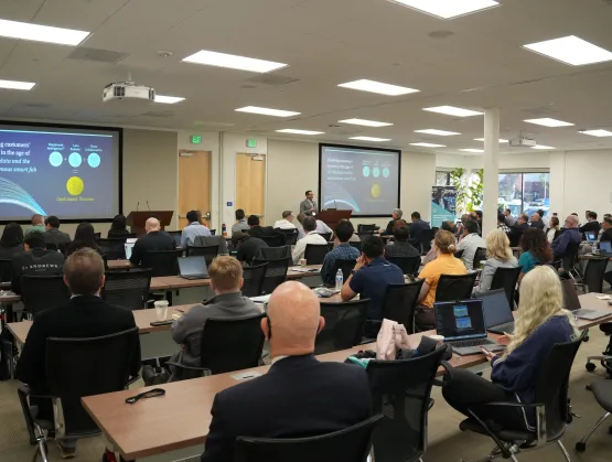
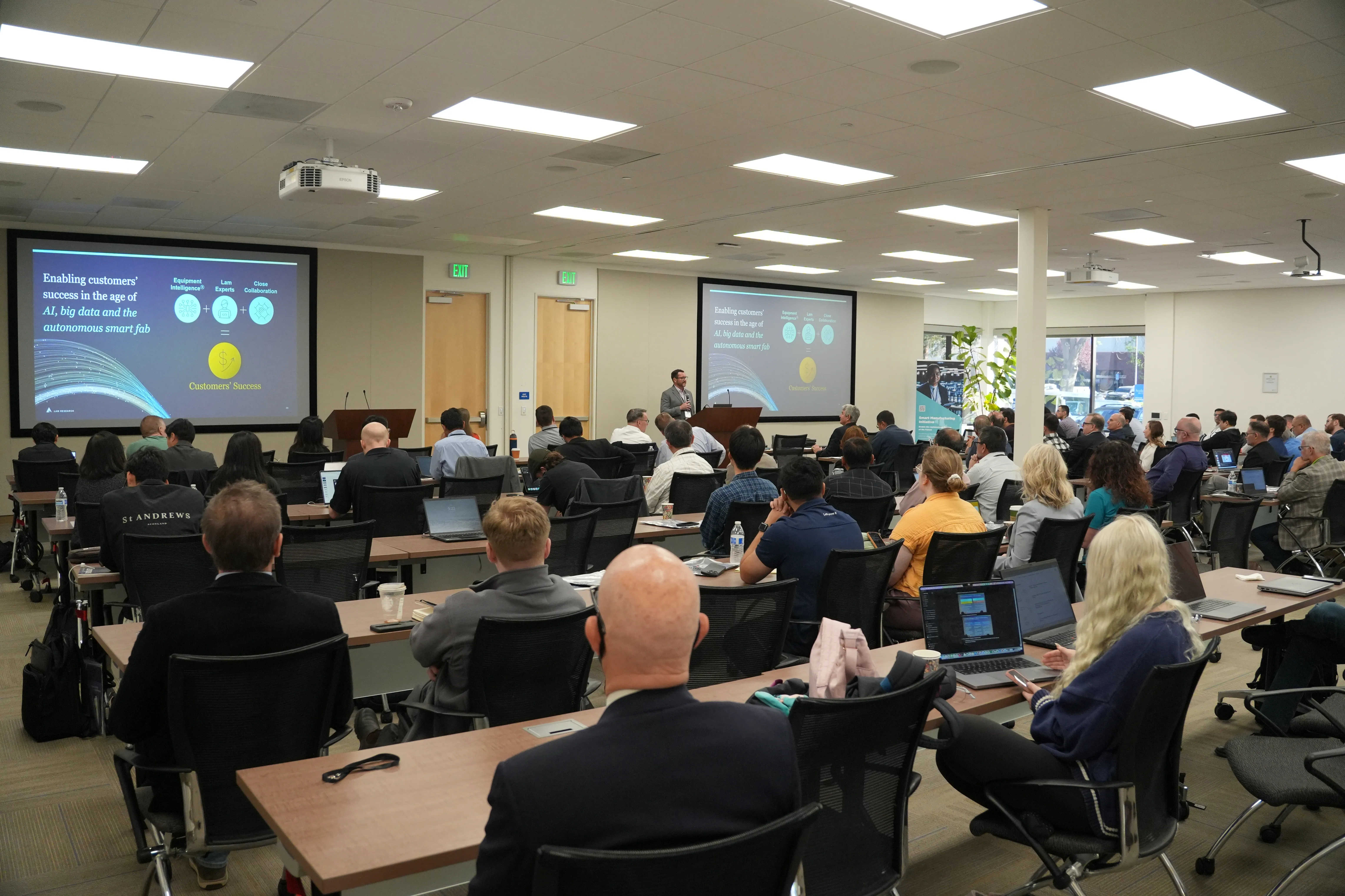
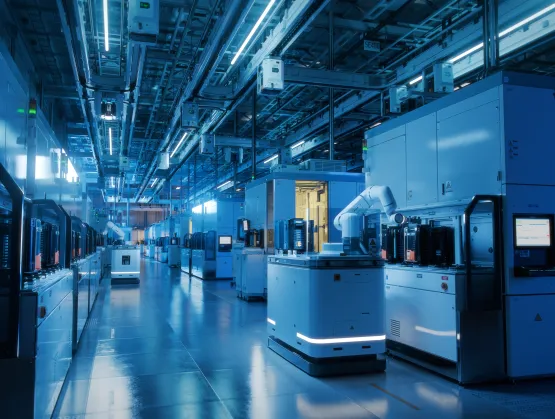
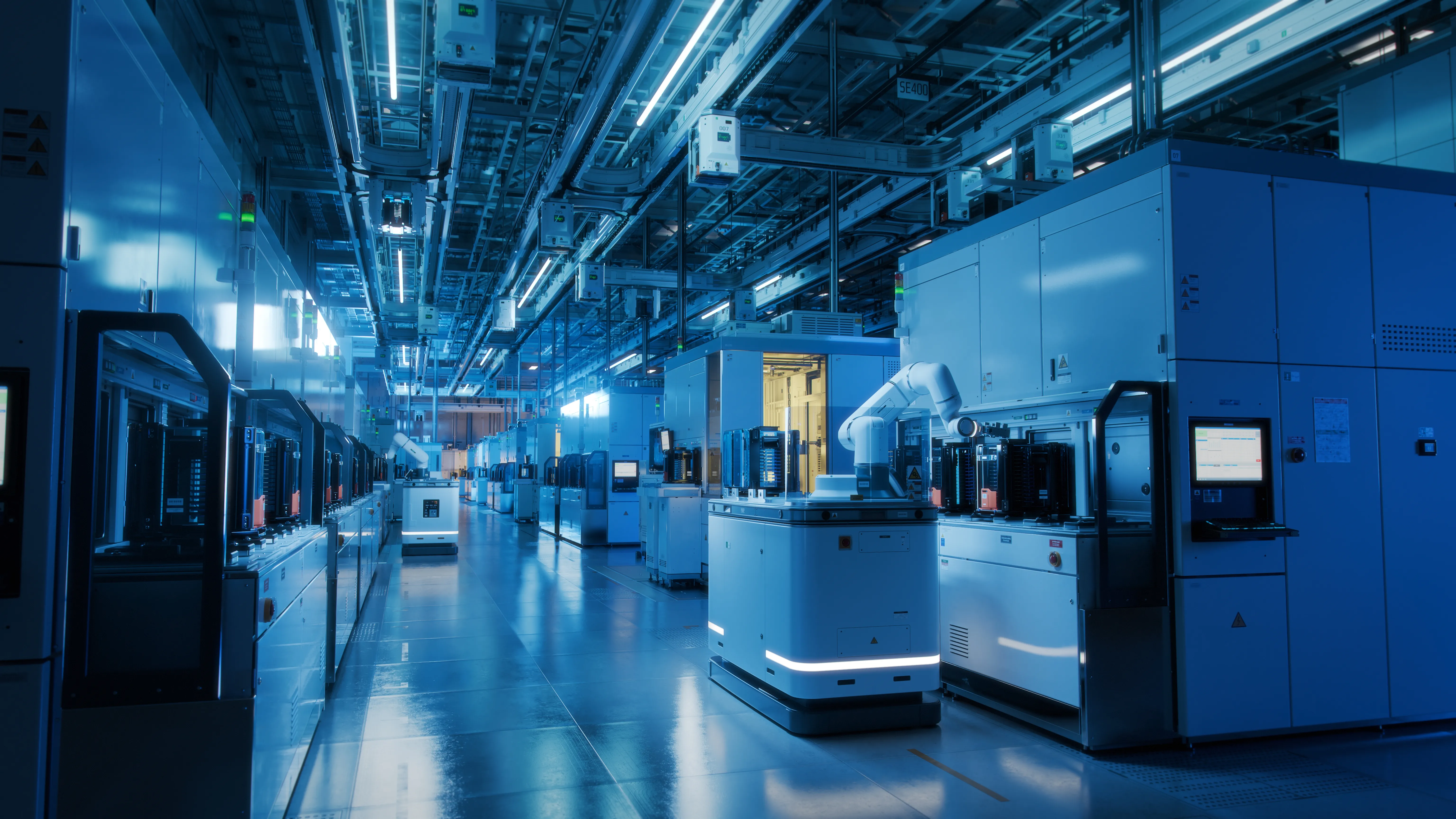
With edge AI emerging as a clear driver of smart manufacturing, SEMI hosted a two-day workshop detailing the future of this technology. The workshop, Smarter Sensors, Smarter Fabs: AI at the Edge in Semiconductor Manufacturing, was held in-person from March 18-19 in Milpitas, California. It convened industry professionals to explore how AI-driven sensors and edge intelligence are fostering scalable and resilient solutions for the next generation of semiconductor manufacturing. The workshop took place across four sessions, with each highlighting a unique edge-AI implementation area – including process control, yield enhancement, tool coordination, and predictive maintenance – and featured keynotes from leaders at Lam Research and KUKA. Didn’t get a chance to attend in person? View this workshop on demand. Session 1 - Smart Sensors and Edge Intelligence for Advanced Process Control​The semiconductor industry has always been defined by precision. However, as device architectures shrink to angstrom-scale dimensions, and as wafers become thinner and more fragile, traditional process control tools are reaching their limits. Sampled, low-frequency, univariate monitoring systems were built for an era where deviations were visible, failures were catchable later, and a handful of sensors per tool were enough to keep yield in check. Session 1 explored the latest sensor technologies, discussing how data collection at the point of production, with AI embedded directly into the tool, is becoming paramount for success. Advanced in-situ sensors were brought up as an example of this in practice. Although these sensors are generating richer signals than in the past, reaching lower latency requires AI models deployed at the edge.In addition, AI is extending into the physical world through robots that can handle various tasks autonomously. These robots are enabled by digital twins that provide simulation environments for training and validation before they ever see the fab floor. The common thread across Session 1 was the growing need for data and knowledge integration in fabs. Smart sensors must be built into AI systems, and those systems must be scalable across tools without sacrificing speed or reliability. Finally, the insights they generate must flow back into maintenance optimization and equipment health monitoring to promote a continuous cycle of learning. Session 2 - Yield Enhancement Through Edge-Driven Defect Detection and Classification​ Session 2 focused on how edge AI models, process sensors, and image data can identify yield-impacting defects earlier in the manufacturing process. As semiconductor devices lean into 3D architectures, the complexity and volume of data have outpaced the capabilities of traditional monitoring tools. Today's fabs are required to evaluate terabytes of inspection images per hour, as well as tool sensor traces that require analysis across dozens of parameters simultaneously. Each speaker approached this challenge from a different angle, yet the solutions fit together into a coherent architecture. One introduced Gaussian Process Regression, a model for assessing both predictions and uncertainties, as a statistically rigorous, data-efficient method for learning "golden trajectory" baselines for tool sensor signals. This generates actionable scores and maintenance guidance beyond standard anomaly alerts. Another speaker demonstrated the ability of deep learning models to triage multi-gigabit-per-second image streams in milliseconds. AI-based defect classification was shown to compress root cause analysis timelines from days to hours, with demonstrated gains of a 0.3% die yield recovery and 0.5–1% yield exposure prevention. Predictive metrology for RF filter frequency also assessed device performance using upstream process data, with less than 0.02% error.Lastly, a software-defined automation framework built on open standards and vendor-neutral architecture demonstrated effective workload consolidation onto a single edge platform. It was shown to be scalable across fabs without replacing legacy infrastructure.These presentations stressed the importance of measurement and action in real-time at the tool level. Gathering information as early as possible, using AI to triage and classify, and feeding insights back into process control and maintenance workflows, allows for a continuous cycle of improvement.Session 3 - Autonomous Work in Process Movement: Robots, Sensors, and Edge AI Coordination​The "lights out" factory is shifting from an aspiration to a concrete, engineering roadmap. To fully realize this, each presentation in Session 3 highlighted the importance of supplementing human-dependent workflows with AI systems that can act in real-time. This shift will require a mix of deep reinforcement learning and AI-based perception approaches. Currently, deep reinforcement learning is training agents to discover new routing strategies that optimize yield, equipment effectiveness, cycle time, and queue-time compliance – including joint front and back-end-of-line coordination for advanced packaging. AI-based perception is also on its way to replacing manual, pre-shipment inspection checklists, demonstrating inspection time reduction by as much as 78%. To enable these improvements, presenters suggested private 5G as the foundational connectivity infrastructure. Currently, private 5G is helping eliminate dead zones and bandwidth issues that are preventing real-time machine data and connected robotics from reaching their full potential.Based on these presentations, the prevailing formula is to integrate intelligence at every level. This includes precise in-situ sensing to eliminate manual setup and measurement, edge AI models that act on data immediately, platforms that coordinate across tools without humans, and lastly, a reliable connectivity infrastructure.Session 4 - Predictive Maintenance at the Edge: From Vibration to VisionSemiconductor fabs have long operated in a state of crisis management. Fab managers spend between 40% and 70% of their time firefighting unexpected equipment failures, rather than executing planned maintenance strategies. Unplanned downtime in semiconductor manufacturing can cost up to $1 million per hour, yet the maintenance industry has been slow to move beyond reactive repairs. Fab managers need faster ways to determine issues and act on that knowledge before wafers are lost. Session 4 outlined a framework for how this transformation will happen. At the foundation, smarter sensors (vibration, acoustic, thermal, spectral, and vision) are generating the high-fidelity, multi-modal data streams that make predictive models possible. In addition, "ultra edge" AI accelerators are enabling machine learning inference to happen directly inside MEMS sensors and on-device hardware without cloud dependency. Fabs require low-latency, data-sovereign, real-time decisions that the cloud is unable to support, and the path forward requires an integrated chain of sensing, edge inference, health scoring, and maintenance scheduling. This session also made the case that irrelevant correlations and confounding variables make purely statistical AI unreliable for root cause analysis, and that causal AI models are required to give fabs actionable information. It concluded that cybersecurity concerns, soaring cloud infrastructure costs (datacenter GPU prices reaching $25,000–$50,000 each in 2025–2026), and latency requirements have made distributed, machine-local intelligence the only viable path to achieving autonomous fabs. SummaryThis workshop highlighted how edge AI, smart sensors, and advanced connectivity are transforming semiconductor manufacturing by enabling real-time process control, faster defect detection, and more autonomous operations. Across sessions, experts emphasized that integrating AI directly at the source of data is essential for improving yield, reducing downtime, and building scalable, resilient “smart fabs.”Learn more by registering for this workshop on demand, or view the recap videos on LinkedIn. Day 1 recap Day 2 recap The SEMI Manufacturing Coalitions include Smart Manufacturing, Fab Owners Alliance (FOA), MEMS and Sensors Industry Group (MSIG), Advanced Packaging Heterogeneous Integration (APHI) and Semiconductor Components, Instruments, and Subsystems (SCIS).Anshu Bahadur leads the Smart Manufacturing Initiative, Karim Somani leads the Fab Owners Alliance (FOA), and Paul Carey leads the MEMS and Sensors Industry Group (MSIG), all of which are part of the Technology Coalitions at SEMI.
Read More
The semiconductor industry is hitting a structural inflection point: explosive AI‑driven demand, rapidly rising manufacturing complexity, and stringent sustainability expectations are converging at once. In this context, edge AI deployed directly on tools, sensors, and local controllers, is shifting from experimental to essential, particularly in fabs where milliseconds matter. SEMI’s timely workshop, Smarter Sensors, Smarter Fabs: AI at the Edge in Semiconductor Manufacturing, taking place March 18–19, 2026 in Milpitas, CA, will address this important topic.From sparse sensing to dense instrumentationTwo decades ago, most process tools relied on dozens of sensors per chamber. Today, leading etch, deposition, CMP, and lithography systems routinely integrate hundreds of sensing channels spanning pressure, flow, RF power, optical endpoint, vibration, and chemistry. At 3 nm and 2 nm, process windows are so tight that yield hinges on multivariate understanding of chamber conditions and tool state rather than a few independent alarms. Sensor proliferation has turned fabs into rich data environments—but also exposed the limits of traditional, centrally managed control.Why edge AI is displacing cloud‑only controlConventional architectures push heavy analytics to centralized servers or the cloud, with supervisory systems periodically updating recipes, setpoints, or dispatch rules. Across manufacturing, measured cloud round‑trip times commonly range from 800 to 2,400 ms, whereas edge systems co-located with equipment can respond in 15–45 ms, roughly 50–160× faster. For safety‑ and yield‑critical loops in semiconductor manufacturing, that latency gap is often unacceptable.At the same time, new generations of low‑power neural processing units (NPUs) and edge accelerators deliver tens of trillions of operations per second (TOPS) at single‑digit watt budgets, making always‑on inference viable inside tools, cameras, and controllers. The result is a decisive move toward edge‑native architectures: models execute where data is produced, while cloud resources are reserved for retraining and fleet‑wide learning.Edge AI on the line: control, inspection, and maintenanceIn process control, edge AI is enabling a shift from univariate threshold checks to multivariate models that understand the joint dynamics of sensor streams. Platforms today embed deep‑learning and statistical models directly at or near the tool, performing real‑time endpoint prediction and anomaly detection from high‑dimensional time series. Similar approaches are emerging in lithography and CMP, where local inference helps keep focus, overlay, and removal rate within spec before wafers drift out of control.Inspection and logistics are undergoing a similar transformation. Vision systems with embedded NPUs classify defects at line speed, often above 100 parts per minute, eliminating the need to ship large image volumes to a central cluster. Robots and autonomous mobile robots (AMRs) use local intelligence for short‑horizon planning and collision avoidance, while higher‑level systems focus on global scheduling and optimization.Predictive maintenance is one of the most mature applications: vibration, acoustic, temperature, and pressure data are analyzed locally to detect anomaly signatures hours or days before conventional thresholds trip. Reported benefits include reductions in unplanned downtime, longer component life, and lower maintenance costs when these models are integrated into manufacturing execution systems (MES) and maintenance workflows.Digital twins and agentic AI on top of edge dataDigital twins build on this sensing and edge‑analytics foundation. By maintaining virtual, live‑updated models of tools, lines, and entire fabs, they enable scenario testing, debottlenecking, and root‑cause analysis without putting WIP at risk. Vendors and early adopters report that such twins can shorten process‑node ramps and facility bring‑up by enabling thousands of “what‑if” experiments before physical changes are made.​Agentic AI is now emerging as the orchestration layer above these twins. In semiconductor case studies, agents connected to MES, advanced process control (APC), and planning systems have delivered double‑digit improvements in throughput, cycle time, and tool utilization by autonomously adjusting routing, batch sizes, and scheduling in response to live fab conditions. Other agents mine unstructured engineering notes and fault reports to accelerate root‑cause analysis, turning hard‑won lessons into repeatable, codified behavior.Sustainability as a first‑class requirementSustainability pressures are reinforcing this stack. Semiconductor manufacturing is energy‑ and resource‑intensive, and regulators and customers alike are demanding more transparency and improvement. Edge‑connected monitoring of energy, utilities, and emissions has already helped some fabs cut energy‑related costs by around 20 percent through tighter control of HVAC, process gases, and idle modes. Research initiatives such as imec’s Sustainable Semiconductor Technologies and Systems (SSTS) program are using virtual fab methods and detailed life‑cycle assessment to guide process and equipment choices for lower environmental impact.Strategic takeaways and where to learn moreThe trajectory is clear: fabs that combine dense sensing, edge AI, digital twins, and agentic AI are building toward continuously learning, self‑optimizing operations. Architectures will need to be edge‑first rather than cloud‑only. Simply adding sensors without local intelligence will not deliver competitive advantage, and environmental KPIs are likely to be optimized with the same rigor as yield and cycle time.For practitioners who want to translate these trends into roadmaps, the Smarter Sensors, Smarter Fabs: AI at the Edge in Semiconductor Manufacturing” workshop (March 18–19, 2026, Milpitas, CA) spearheaded by the SEMI Manufacturing Coalitions* will bring together experts in sensing, edge architectures, digital twins, and agentic AI to share concrete deployments and architectures tailored to semiconductor fabs.*The SEMI Manufacturing Coalitions include Smart Manufacturing, Fab Owners Alliance (FOA) MEMS and Sensors Industry Group (MSIG), Advanced Packaging Heterogenous Integration (APHI) and Semiconductor Components, Instruments, and Subsystems (SCIS). Anshu Bahadur is Senior Program Manager, Technology Communities at SEMI. Mark da Silva is Senior Director, Manufacturing Coalitions at SEMI.
Read More
While Artificial Intelligence (AI) emerged in the 1950s, only in recent years have AI applications proliferated with the explosion of data and continuing improvements in Moore’s law that have driven rising processing speeds. Voice assistants, image analysis software, search engines, and speech and facial recognition systems were among the first applications to use AI. Today, adoption has spread to sectors such as agriculture, cybersecurity, healthcare, software development, e-government and the intelligent enterprise to generate jobs and help spur economic growth. The Edge AI Opportunity and the Microelectronics IndustryAI can be embedded in hardware devices such as advanced robots, autonomous cars, drones or Internet of Things (IoT) applications. Today, according to the EU’s digital strategy, data centres and other centralized computing facilities account for the vast majority – 80% – of AI data processing and analysis, with smart connected objects such as automobiles, home appliances and manufacturing robots that bring the compute function closer to the user representing 20%. The latter, known as Edge AI applications, are powered by edge-based machine learning chipsets, not the AI chipsets designed to run cloud-based machine learning algorithms.The EU’s white paper on AI published in February 2020 anticipates that the way data are stored and processed for AI applications will change significantly over the coming five years as edge computing applications proliferate. Most AI applications need to connect with devices that collect data and manage data flows. When the applications connect with cloud infrastructures to train large volumes of data for a machine learning model, the interface devices often require hardware support. Edge AI can minimize data transport by processing data directly from local devices to accelerate data analysis and decision-making and make data transport or accelerator hardware unnecessary, critical in reducing power consumption and enhancing data security for applications such as autonomous driving. Over the past 40 years, the ICT sector has been continuously increasing greenhouse gas (GHG) emissions despite efforts to shift to renewable energy. Cloud-based AI applications require an ICT infrastructure for high-performance computing and high-speed connectivity. According to MIT Technology Review, data centres’ AI workloads could account for a tenth of the world’s electricity usage by 2025. a mass update of cloud-based AI applications may significantly increase energy consumption, unlike with Edge AI. This is why the strategy for developing Edge AI is well-aligned with the EU’s Green Deal objectives. Europe aspires to play a leadership role in Edge AI to strengthen the sector’s competitiveness and protect the European digital sovereignty. Europe’s strong industrial competencies in embedded systems and microcontrollers will help the region promote development of European domestic AI solutions for emerging high-value IoT applications in industrial processes such as Industry 4.0, Connected and Automated driving (CSA), smart cities, climate action, healthcare, and national defence and security. With this strong strategic position in technology, Europe is well-positioned to invest to become the leader in the Edge AI global market.Preparing the Workforce for the Microelectronics IndustryTo design and manufacture leading Edge AI chipsets, European education providers and industry will need to work closely together to train the current and future workforces. Within the framework of the METIS project, a four-year project co-funded by the European Commission through the Erasmus+ programme, SEMI and imec deployed experts in the field to survey and interview focus groups. The survey identified the following key focus areas for workforce development: 1. True Capability of AI and Data Science With AI’s heavy dependence on data, the workforce of the future must be trained in areas of data science including data integrity to ensure quality, unbiased sourcing, collection and accurate analysis necessary to interpret huge volumes of data. Europe also needs to train the next generation of AI chip designers in data security and privacy – key challenges to the widespread deployment of Edge AI chips. 2. Climate Change, Sustainable Development Goals (SDGs) and Social Inclusion TrainingSince the industry must be able to develop Edge AI solutions to enable the digital transformation while limiting GHG emissions, microelectronics engineers need to be schooled in climate change and understand how their work contributes to meeting the United Nation’s Sustainable Development Goals (SDGs). Workplace diversity and social inclusion are also important target areas for education since Edge AI applications should serve various groups of people with different needs.3. EthicsChip industry workers must also be educated in ethical issues of AI related to the technology’s potential societal impact in the near future[1]. With AI applications capable of monitoring Internet searches based on users’ personal preferences and biases to deliver tailored advertising, news and other information, developers must recognize how the technology can influence thinking and behaviour of individuals and groups. This awareness can help developers strike a balance between supporting commercial interests and societal good so the microelectronics industry can ensure ethical implementation of AI. 4. Cross-disciplinary Skills Required for AIAI development requires a comprehensive, cross-disciplinary skill-set to be able to integrate the work of specialists from diverse educational, cultural and professional backgrounds critical to developing non-biased AI solutions. For example, in addition to technical expertise, microelectronics AI developers must be able to communicate clearly and work in close-knit teams with non-technical experts from business, law, medicine and the social sciences.What’s Next?The microelectronics industry has a tremendous opportunity to develop new chip-based solutions for AI architectures, and apply AI techniques to improve operational efficiencies of design and manufacturing. To seize this opportunity, the industry must work closely with education providers to groom the next generation of skilled workers. This tight collaboration is critical to designing and delivering specialised courses to college and university students as well as engineers now working in the chip sector. The stakes are high. By preparing workers to develop Edge AI chipsets, the microelectronics industry can help the world confront some of the greatest challenges it faces today.For more information, see SEMI Responds to European Commission White Paper on Artificial Intelligence.METIS is a Sector Skills Alliance project co-funded by the European Commission’s Erasmus+ Program and coordinated by SEMI. The four year project, launched in November 2019, will develop a Microelectronics Skills Strategy. Based on the strategy, the METIS project will design 43 training modules for 1,100 hours learning in four key areas of the microelectronics sector.We thank Patrick Blouet (STMicroelectronics) and Jeroen Geusens (imec) for their valuable contributions to this article.[1] Ethics of Artificial Intelligence and Robotics, Stanford Encyclopedia of PhilosophyDr. Yanying Li is senior manager of Collaborative Projects at SEMI Europe.Dr. Pushkar P. Apte is the strategic technology advisor for the Smart Data AI Initiative at SEMI
Read More
Europe is facing an acute shortage of skilled microelectronics workers that undermines the growth potential of not only the electronics industry but the European economy as a whole. Nearly 1.1 million job advertisements for electro-engineering workers were placed in the EU between mid-2018 and the end of 2019 (CEDEFOP, 2020). The shortfall looms large as a skilled and diverse workforce that can continuously innovate is the oxygen of microelectronics. In light of the critical importance of microelectronics to Europe’s ability to fulfill its growth potential, SEMI Europe participated in the high-level roundtable hosted by Commissioner Nicolas Schmit and Commissioner Thierry Breton on October 5. The discussion’s key takeaway: The skills challenge facing the microelectronics industry is too complex for one organization to tackle, and reskilling and upskilling its workforce should be a common priority for Europe. Only with a diverse, substantial and skilled microelectronics workforce can Europe achieve its R D, design and manufacturing ambitions while ensuring its sovereignty in the digital age. The roundtable highlighted the EU Pact for Skills as a key means to narrow the industry’s skills gap.An ever-growing part of our lives, microelectronics, with their ability to run billions of computations per second and store vast quantities of data, are the brains of modern technology. The digital sovereignty of nations around the world today relies on advanced microprocessors to collect, transfer, analyze and store immense amounts of data used in key end-user sectors such as mobility, telecommunications, energy, security and healthcare. Information and communication technologies (ICT) enabled by microelectronics are helping much of the world’s population to work and study from home and remain safe during the COVID-19 pandemic.According to the Smarter2030 Report, further deployment of ICT, including electronic components in critical sectors such as transportation, manufacturing, agriculture, construction and energy, could eliminate the equivalent of 12.1 billion tons of CO2 per year globally. These are some of the reasons why nations worldwide are making large-scale investments to advance a homegrown microelectronics R D, design and manufacturing base. It is no surprise, then, that semiconductors are now at the center of the so-called global techno-trade wars.Clearly, Europe urgently needs to mobilize and pool resources to develop effective lifelong learning programs for all workers and continue investing in microelectronics innovation. We need to instill the passion for creating technology among current and future workforce, in particular women and people with challenged backgrounds, and build a highly diverse talent pool. Working together, we can better demonstrate how computing technologies, including quantum, high-performance and edge AI, provide solutions to grand societal challenges and attract talented people to the fascinating world of electronic components and systems.Against this backdrop, the microelectronics industry finds the Pact for Skills very timely and crucial to advancing the talent pool underpinning Europe’s deep digital ecosystem. The Pact will play an instrumental role in improving the scope and the quality of training partnerships at regional, national and European levels, sharing best practices and helping the microelectronics industry and workforce adapt to the effects of COVID-19.The microelectronics industry is committed to building on the momentum created by the METIS Erasmus+ collaborative project and to mobilizing our ecosystem and education partners for a successful Pact for Skills in Microelectronics starting this year.The High-Level Roundtable: Skills for Microelectronics was hosted by Commissioner Thierry Breton and Commissioner Nicolas Schmit. Participants included Paul Boudre, CEO, SOITEC; Lars Reger, CEO Germany and CTO, NXP; Frits van Hout, Executive Vice-President and Chief Strategy Officer, ASML; Françoise Chombar, CEO, Melexis; Emmanuel Sabonnadiere, CEO, CEA-Leti; Luc Van den hove, President and CEO, imec; Sabine Nietzsche, Board member, Silicon Saxony and Vice President, GlobalFoundries; Laith Altimime, President, SEMI Europe (coordinator of METIS); Yolande Berbers, President, European Society for Engineering Education (SEFI); James Calleja, President, European Forum for Technical Vocational Education and Training (EFVET); Ludovic Voet, Confederal Secretary, European Trade Union Confederation (ETUC).Emir Demircan is director of Advocacy and Public Policy at SEMI Europe. To learn more about SEMI Europe advocacy, contact Emir at [email protected].
Read More