downloadGroupGroupnoun_press release_995423_000000 copyGroupnoun_Feed_96767_000000Group 19noun_pictures_1817522_000000Member company iconResource item iconStore item iconGroup 19Group 19noun_Photo_2085192_000000 Copynoun_presentation_2096081_000000Group 19Group Copy 7noun_webinar_692730_000000Path
Skip to main content
Default Banner Image

edge computing

While Artificial Intelligence (AI) emerged in the 1950s, only in recent years have AI applications proliferated with the explosion of data and continuing improvements in Moore’s law that have driven rising processing speeds. Voice assistants, image analysis software, search engines, and speech and facial recognition systems were among the first applications to use AI. Today, adoption has spread to sectors such as agriculture, cybersecurity, healthcare, software development, e-government and the intelligent enterprise to generate jobs and help spur economic growth. The Edge AI Opportunity and the Microelectronics IndustryAI can be embedded in hardware devices such as advanced robots, autonomous cars, drones or Internet of Things (IoT) applications. Today, according to the EU’s digital strategy, data centres and other centralized computing facilities account for the vast majority – 80% – of AI data processing and analysis, with smart connected objects such as automobiles, home appliances and manufacturing robots that bring the compute function closer to the user representing 20%. The latter, known as Edge AI applications, are powered by edge-based machine learning chipsets, not the AI chipsets designed to run cloud-based machine learning algorithms.The EU’s white paper on AI published in February 2020 anticipates that the way data are stored and processed for AI applications will change significantly over the coming five years as edge computing applications proliferate. Most AI applications need to connect with devices that collect data and manage data flows. When the applications connect with cloud infrastructures to train large volumes of data for a machine learning model, the interface devices often require hardware support. Edge AI can minimize data transport by processing data directly from local devices to accelerate data analysis and decision-making and make data transport or accelerator hardware unnecessary, critical in reducing power consumption and enhancing data security for applications such as autonomous driving. Over the past 40 years, the ICT sector has been continuously increasing greenhouse gas (GHG) emissions despite efforts to shift to renewable energy. Cloud-based AI applications require an ICT infrastructure for high-performance computing and high-speed connectivity. According to MIT Technology Review, data centres’ AI workloads could account for a tenth of the world’s electricity usage by 2025. a mass update of cloud-based AI applications may significantly increase energy consumption, unlike with Edge AI. This is why the strategy for developing Edge AI is well-aligned with the EU’s Green Deal objectives. Europe aspires to play a leadership role in Edge AI to strengthen the sector’s competitiveness and protect the European digital sovereignty. Europe’s strong industrial competencies in embedded systems and microcontrollers will help the region promote development of European domestic AI solutions for emerging high-value IoT applications in industrial processes such as Industry 4.0, Connected and Automated driving (CSA), smart cities, climate action, healthcare, and national defence and security. With this strong strategic position in technology, Europe is well-positioned to invest to become the leader in the Edge AI global market.Preparing the Workforce for the Microelectronics IndustryTo design and manufacture leading Edge AI chipsets, European education providers and industry will need to work closely together to train the current and future workforces. Within the framework of the METIS project, a four-year project co-funded by the European Commission through the Erasmus+ programme, SEMI and imec deployed experts in the field to survey and interview focus groups. The survey identified the following key focus areas for workforce development: 1. True Capability of AI and Data Science With AI’s heavy dependence on data, the workforce of the future must be trained in areas of data science including data integrity to ensure quality, unbiased sourcing, collection and accurate analysis necessary to interpret huge volumes of data. Europe also needs to train the next generation of AI chip designers in data security and privacy – key challenges to the widespread deployment of Edge AI chips. 2. Climate Change, Sustainable Development Goals (SDGs) and Social Inclusion TrainingSince the industry must be able to develop Edge AI solutions to enable the digital transformation while limiting GHG emissions, microelectronics engineers need to be schooled in climate change and understand how their work contributes to meeting the United Nation’s Sustainable Development Goals (SDGs). Workplace diversity and social inclusion are also important target areas for education since Edge AI applications should serve various groups of people with different needs.3. EthicsChip industry workers must also be educated in ethical issues of AI related to the technology’s potential societal impact in the near future[1]. With AI applications capable of monitoring Internet searches based on users’ personal preferences and biases to deliver tailored advertising, news and other information, developers must recognize how the technology can influence thinking and behaviour of individuals and groups. This awareness can help developers strike a balance between supporting commercial interests and societal good so the microelectronics industry can ensure ethical implementation of AI. 4. Cross-disciplinary Skills Required for AIAI development requires a comprehensive, cross-disciplinary skill-set to be able to integrate the work of specialists from diverse educational, cultural and professional backgrounds critical to developing non-biased AI solutions. For example, in addition to technical expertise, microelectronics AI developers must be able to communicate clearly and work in close-knit teams with non-technical experts from business, law, medicine and the social sciences.What’s Next?The microelectronics industry has a tremendous opportunity to develop new chip-based solutions for AI architectures, and apply AI techniques to improve operational efficiencies of design and manufacturing. To seize this opportunity, the industry must work closely with education providers to groom the next generation of skilled workers. This tight collaboration is critical to designing and delivering specialised courses to college and university students as well as engineers now working in the chip sector. The stakes are high. By preparing workers to develop Edge AI chipsets, the microelectronics industry can help the world confront some of the greatest challenges it faces today.For more information, see SEMI Responds to European Commission White Paper on Artificial Intelligence.METIS is a Sector Skills Alliance project co-funded by the European Commission’s Erasmus+ Program and coordinated by SEMI. The four year project, launched in November 2019, will develop a Microelectronics Skills Strategy. Based on the strategy, the METIS project will design 43 training modules for 1,100 hours learning in four key areas of the microelectronics sector.We thank Patrick Blouet (STMicroelectronics) and Jeroen Geusens (imec) for their valuable contributions to this article.[1] Ethics of Artificial Intelligence and Robotics, Stanford Encyclopedia of PhilosophyDr. Yanying Li is senior manager of Collaborative Projects at SEMI Europe.Dr. Pushkar P. Apte is the strategic technology advisor for the Smart Data AI Initiative at SEMI
Read More
Not long after STMicroelectronics opened its first semiconductor plant in Singapore more than 50 years ago, a facility chiefly focused on chip assembly and packaging, the company realized that it had constructed the site in an area with a blossoming chip ecosystem with a bright future. Before long, the company became the first to start a wafer fab facility in the so-called Little Red Dot. Today, our STMicroelectronics Singapore campus sports several buildings that dwarf the original site in the sprawling Ang Mo Kio Industrial Park 2. The facilities feature advanced 200mm manufacturing lines but still produce huge volumes of chips with more than 1,000 pieces of 150mm manufacturing equipment.Much of the wafer equipment dates back to the past century so is no longer supported by the manufacturers, if they’re still even in existence. Yet decades later the chipmaking gear continues to operate with a surprising reliability that far surpasses the longevity called for in its manufacturing specifications thanks to replacement parts and frequent upgrades with more sophisticated handling robots and chucks. Now, as smart manufacturing begins to establish a foothold in the semiconductor industry, Industry 4.0 technology is breathing new life into these aging workhorses.Despite its age, all of the equipment adheres to industry manufacturing standards. The gear is remotely controlled using the SECS/GEM interface protocol that was either originally integrated with the equipment controller or custom-made. We’ve also maximized its usage through advanced recipe management, advanced alarm and event handling, and secured lot identification.Crucially, we decided to systematically deploy a real-time fault detection and classification (FDC) solution using a third-party product based on what today is known as an edge computing architecture. Every piece of critical processing equipment is progressively paired with its dedicated FDC instance running on a virtual machine in the wafer fab data center, and the FDC solution monitors vital equipment parameters at high frequency – depending on the SECS/GEM capabilities of the equipment – and analyzes incoming manufacturing data in real time using classic SPC (statistical process control) algorithms and even AI-class protocols.Our use of the FDC edge solution as a sensor signal aggregator has given our equipment a second life. The solution processes real-time signals from sensors connected through a typical TCP-IP. Sensors have been the old equipment’s saving grace with their ability to de-multiply equipment capabilities and overcome fundamental shortcomings and design weaknesses. The STMicroelectronics Singapore plant first used off-the-shelf sensor nodes with built-in power amplifier and analog input nodes. While very practical and easy to implement, deploying the nodes can be costly. After developing more expertise in sensor integration using FDC, our wafer fab equipment experts decided to design an in-house solution based on the famed STM32 microcontroller. Leveraging Arduino – an open-source electronics platform with easy-to-use hardware and software – the equipment teams can now design and program a variety of in-house sensors for measurements including temperature, humidity, waterflow and pressure. The sensors are integrated with process equipment using the FDC solution. Integrating the sensors with the FDC engine on the edge computer extends the capabilities of old equipment without jeopardizing the integrity of the machines themselves. While the integration can be quick, it must be robust to ensure the reliability of the new measurements. Similarly, ever-increasing connectivity requirements present clear cybersecurity risks that must be managed upfront and each solution must be hardened to minimize security vulnerabilities. Even so, the challenges and risks pale in comparison to the benefits! Jean-Marc PHILIPPE is DIT Director at STMicroelectronics Pte Ltd. He oversees the deployment and support of Digital Solutions to enable STMicroelectronics front-end operations in Singapore and manages manufacturing productivity and automation programs at site level.
Read More
Software for sensors has evolved from simply reading out and evaluating sensor data to making intelligent decisions based on that data, a transformation enabled by new software synthesis and artificial intelligence (AI) technologies. Together, they make consumer devices smarter, dramatically improving the user experience through greater interactivity and higher levels of automated personalization.SEMI’s Nishita Rao spoke with Stefan Finkbeiner, CEO and General Manager at Bosch Sensortec, who will explore the topic in his October 23 keynote, How Software Makes MEMS Sensors into Smart Systems, at MEMS Sensors Executive Congress (MSEC), October 22-24, 2019, at the Coronado Island Marriott Resort Spa in Coronado, Calif.Join us at MSEC to meet Bosch Sensortec and other industry influencers driving MEMS and sensors innovations. Registration is open.SEMI: What is the relationship between MEMS sensors suppliers and specialized software synthesis providers?Finkbeiner: Collaboration is a key driver for innovation in sensor software. There are already several fruitful collaborations between MEMS sensors suppliers and specialized software providers, which are mostly startups. Collaborations with providers of simulation and evaluation tools as well as with well-known universities in the field of AI are starting to show positive results.Domain expertise is also critical for developing smart sensor software, making it essential to future sensing solutions.SEMI: How does software synthesis relate to sensor fusion?Finkbeiner: Put simply, software synthesis refers to ways of automatically generating code based on domain knowledge and given constraints for specific product versions. Sensor fusion combines sensor data from different kinds of sources in order to improve the results.Software synthesis techniques enable a level of automation that creates new opportunities for more complex sensor fusion, which was formerly out of reach when using traditional approaches that involved, for example, big data and a large number of potential data sources.The traditional sensor fusion toolset can now be further extended by machine learning techniques that help to determine which sources are more reliable than others and how to combine data streams. This topic and others are still active areas of research. A wearable device with motion detection is a case in point. With unsupervised learning, the device could identify short versus long cyclically repeating motions and treat them differently from other types of motion. SEMI: How is the new software synthesis-AI approach different from previous approaches? To what degree will the new approach open up new applications?Finkbeiner: Traditionally, technology companies have used cloud computing for data storage and machine learning on aggregated user data. In that model, MEMS sensors generate large amounts of data that power-hungry hardware (such as digital signal processors) must process. In addition, machine learning generally requires lots of power-hungry cloud nodes with GPUs. This model, however, is not the best option for many users. Just think for a moment about all the scenarios in battery-powered devices where frequent battery charging frustrates users.Leveraging both software synthesis and AI techniques in MEMS sensors is therefore a very promising approach because it supports improved recognition and learning inside the sensor. This means that user-specific data isn’t transferred to the cloud. Instead, it remains private inside the sensor. This improves existing applications that learn all the time and opens up new opportunities for applications such as smart clothing, predicting a product’s lifespan, detecting whether a window or door is open or closed – all without server connectivity.SEMI: How will such software adapt to the individual user?Finkbeiner: Devices will offer much more personalized information to users. For example, optimizing a step counter to match the height, age or Body Mass Index (BMI) of a user – or to adapt to a user’s environment (is the person running on a beach, hiking up a mountain or strolling in a park?) – will provide more accurate information on calories burned. Not every step is created equal, and both pre-loaded personal data as well as real-world environmental data will prove that some steps consume a lot more energy than others.SEMI: What would you like MSEC attendees to take away from your presentation?Finkbeiner: I want to introduce the journey of software development by illustrating specific use case examples. I would also like to offer my outlook on the role of software and AI in MEMS sensors to help increase their adoption in current and new applications. Ultimately, I think it’s important to raise awareness in our industry on why we should embrace the use of software and AI.Connect with Stefan Finkbeiner at MSEC or via LinkedIn. Get more information on Bosch Sensortec products and solutions online.Stefan Finkbeiner, Ph.D., CEO and General Manager, Bosch Sensortec, was appointed CEO of Bosch Sensortec in 2012. He joined the Robert Bosch GmbH in 1995 and has been working in different positions related to the research, development, manufacturing, and marketing of sensors for more than 20 years. His senior positions at Bosch have included director of marketing for sensors, director of corporate research in microsystems technology, and vice president of engineering for sensors.Finkbeiner received his Diploma in Physics from the University of Karlsruhe in 1992 before studying at the Max-Planck-Institute in Stuttgart, where he earned his Ph.D. in Physics in 1995. In 2015, Finkbeiner received the prestigious lifetime achievement award from the MEMS Sensors Industry Group (MSIG), a SEMI technology community.Bosch Sensortec is a member of MEMS Sensors Industry Group, the industry association representing the global MEMS and sensors supply chain. To learn more about how MSIG enables professionals in the MEMS and sensors industry to innovate, address common challenges and accelerate business results, visit us today.Nishita Rao is marketing manager for technology communities at SEMI.
Read More
For nearly two decades, Sean Ding, CTO and chief scientist of Alibaba Cloud IoT, has worked in software and algorithm architectures, sensing, semiconductors, systems and cloud computing – all areas that have contributed to the rise of the Internet of Things (IoT). It’s no surprise, then, that Alibaba is leading next-generation innovation for the IoT. Ding will bring his expertise to his role as moderator of Brave New World - MSIG Conference on AI+IoT 2019, a half-day forum March 20, 2019, at SEMICON China in Shanghai, China. Maria Vetrano of SEMI spoke with Ding about technologies key to the IoT era including MEMS, sensors, artificial intelligence (AI), edge gateways and cloud computing. SEMI: MEMS sensors are widely used in IoT devices. What is the relationship between AI and MEMS sensors?DING: While MEMS sensors and AI will increasingly co-reside in end-user devices, I do not recommend adding AI next to the sensor (in the same package). That’s because designers continue to use the ASIC for signal conditioning, so A/D converters are still required. Rather, we should look to edge gateways to carry the majority of the workload, including deep learning, because this reduces system complexity and power consumption.SEMI: Why are smarter sensors shifting data processing and analytics to the edge of IoT devices?DING: Data processing and analytics are very important for IoT devices, but we need to focus on understanding the data, parameter calibration and more. The MEMS sensor industry should leave big data analytics to edge computing and cloud computing because AI requires deep learning, demanding a huge amount of data.The challenge is to find the sweet spot for data processing right next to the sensor element.SEMI: What is China’s evolving role in innovation in MEMS sensors for IoT devices?DING: At present, the MEMS community in China needs to figure out how to innovate instead of copying existing technologies, a low-margin business that will not help to grow the industry. One reason why I am so pleased to see the MSIG Conference on AI+IoT in China is that it will encourage greater creativity in the MEMS community in China, and this will ultimately lead to Chinese companies and R D institutions leading innovation rather than copying it.SEMI: What is the right approach to combining smart MEMS sensors with AI in IoT devices? Why is this important for both domestic Chinese and international markets?DING: Combining data from sensors with cloud-edge computing is the right approach. As sensor companies increasingly provide end-to-end solutions, such as “sensor+ firmware + SaaS + app,” we will realize easier and faster integration of sensors in IoT applications.This is incredibly important because China today is the world’s biggest market for IoT hardware. China has 2,000-plus design houses, 200-plus OEMs and thousands of distributors. That said, we still see a highly fragmented market that will benefit from a faster integration methodology.Faster integration of MEMS sensors and AI/machine learning for IoT hardware will benefit designers in international markets as well.SEMI: What do you hope MISG Conference on AI+IoT attendees will take away from the forum? DING: MEMS sensors are highly fragmented, reflecting the highly fragmented applications in which they play. The MEMS sensors industry should figure out how to provide one-stop-shopping solutions for vertical markets. This will speed the scalability of applications and expedite the growth of sensor production. Sean Ding (柯镇) will moderate Brave New World - MSIG Conference on AI+IoT 2019 at SEMICON China on Wednesday, March 20, 2019, at Kerry Hotel Pudong in Shanghai, China.This conference has been organized by the MEMS Sensors Industry Group (MSIG). Register today to connect with Sean Ding and featured speakers at the event.Speakers at the MSIG Conference on AI+IoT 2019 at SEMICON China include: Welcome and Introduction / 欢迎辞Carmelo Sansone, Director, MEMS Sensors Industry Group (MSIG), a SEMI technology community AI Needs Accurate Data – MEMS Sensors Can Provide It / MEMS传感器为人工智能提供真实数据Andrea Onetti, Group VP of Analog MEMS Group, GM of MEMS Sensor Division, STMicroelectronics Enhanced IoT Edge by Smart Sensors / 智能传感器助力IoT边缘智Bennini Fouad, Regional President Asia Pacific, Bosch Sensortec Horizon AI Processor Solution, Enable Industries in AI Time / 地平线AI芯片解决方案,赋能千万业Carl Zhang 张永谦, General Manager/VP, Smart Chip Solutions Division, Horizon Robotics Inertial Sensors in AI Applications / 运动传感器AI应用案例Ben Lee 李彬 , CEO, mCube Ultra-Low-Power Solutions: an Ecosystem Approach / 超低功耗的生态链解决方案Carlos Mazure, IEEE Fellow, Chairman Executive Director, SOI Industry Consortium High-Integrity, Fault-Tolerant Open Inertial Measurement Platform for AI-based Vehicle Automation / 适用于人工智能车辆自动控制的高集成及容错的惯性测量开放平台Dan Dempsey, Senior Director of Automotive, ACEINNA Maria Vetrano is a public relations consultant at SEMI.
Read More
The more than 53,000 people who flocked to SEMICON Korea last month were treated to a motherlode of insight into the future of the semiconductor industry as 470 companies exhibited innovative technologies in more than 2,000 booths. But the annual event’s most arresting numbers came in keynotes and other presentations pointing to the extraordinary industry growth that lies ahead.“It is no exaggeration to say that 90 percent of the world’s data has been generated in the last few years,” said Jim Feldhan, president of Semico Research. “This explosive growth of data is expected to continue. That's why server shipments will grow by 20.3 percent, or 30 million units, this year alone.”Feldhan said that the Internet of Things (IoT) will be a chief driver of semiconductor industry growth, with IoT expected to be applied in areas as varied as automotive, smart cities, edge computers, finance, architecture, agriculture and healthcare. For its part, artificial intelligence (AI) will start to exercise human-like judgment. Feldhan noted that in many instances in these fields, “it is more accurate to apply AI and vision systems than to rely on traditional decision-making.”Yoon Jong Lee, senior vice president of DB HiTek, predicted that the Internet, AI and 5G will drive market growth. “Looking back over the past 30 years, semiconductor market growth was powered by PCs, the Internet and cell phones, yet last year memory accounted for 35 percent of total semiconductor sales, more than double the figure in 2016,” he said. He predicted that, in 2019, the foundry sector will outstrip the semiconductor market in growth, noting that the average growth rate of the semiconductor industry is expected to be 4.1 percent, compared to 7.1 percent for the foundry market. Clark Tseng, director of SEMI, reported that the strong semiconductor growth in 2018 is unlikely to continue in 2019 due to the decline in memory pricing, as well as mobile and PC demand. “Demand for semiconductors is likely to decline in the first half as the industry is still digesting inventory and rebound in the second,” Tseng said. Semiconductor industry growth headwinds include decreases in high-end smartphone purchases, PC demand and demand for DRAMs for servers in data centers, Tseng said. Declines in economic growth and consumption in China and the U.S.-China trade war will also contribute to a slowdown. However, Tseng noted that, over the long term, technology innovation will continue and that the semiconductor industry’s prospects remain bright.One key innovation will be the elimination of AI’s reliance on Internet connections in the future. In his opening day keynote, Eunsoo Shim, senior vice president at Samsung Electronics, emphasized that AI technology that operates without the Internet in the future is essential. “We are developing 'on-device AI' technology that incorporates AI algorithms in products such as smartphones and autonomous vehicles,” he said. "When on-device AI technology is implemented, it reduces reliance on the Internet, battery consumption, and data latency.” Reducing latency will significantly improve device response time.Walden C. Rhines, CEO Emeritus of Mentor, a Siemens business, predicted that AI will fuel rapid memory growth. The memory semiconductor (DRAM, NAND flash) market is expected to see a temporary slowdown this year, with the market expected to rebound in 2020. Rhines said that memory could be seen as an early market with rapid future growth, citing memory market super-booms in 1995 and 2000.“Memory production has not decreased since 1995 or 2000,” he said. “Although memory prices will temporarily fall this year after significant market growth in 2017 to 2018, the market will continue to grow as memory production increases,” he said. Rhines added that “although memory prices will drop by about 10 percent this year, he believes prices will increase 6 percent next year.” He also predicted the steady growth of the non-memory semiconductor market as AI technology matures and China’s investment in fabless companies continues.Indeed, SEMICON Korea speakers made it clear that concerns about the growth of the semiconductor industry are expected to be short-lived. While overall growth is likely to slow in 2019, the industry is expected to rebound steadily – powered by the semiconductor industry paradigm shift led by AI, IOT, and autonomous driving – and reach a new high of nearly $541 billion in 2020.Jaegwan Shim is a marketing specialist at SEMI Korea.
Read More
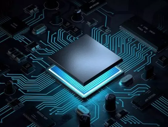
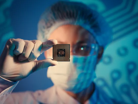
Ahead of his presentation on the future of wearables at the European MEMS Sensors Summit 2018, 19-21 September in Grenoble, France, SEMI spoke with Dr. Peter Weigand, vice president, Business Strategy and Portfolio Management, Bosch Sensortec GmbH. Dr. Weigand gave a glimpse into insights he’ll share at the event.1. Wearables such as smartwatches, fitness trackers or hearables are becoming ubiquitous – but what are the must-haves for wearables for daily use by wearers?We see that users nowadays want to track their activities such as steps walked, calories burnt and floor levels “climbed” on a daily and holistic basis. “Quantifying yourself” is becoming an overall trend in our society with health, fitness and well-being continuously gaining in importance. This is only possible if information about activities is delivered comprehensively in an accurate manner. Therefore, at Bosch Sensortec we provide MEMS sensors that measure the user’s activity very precisely. For example, the smart sensor hubs BHI260 and BHA260 provide sophisticated in-sensor algorithms (e.g. activity recognition) with very low latency and guaranteed performance due to the real-time nature of the embedded software. From the system manufacturer’s perspective, “quantifying yourself” on a 24/7 basis means that the device has to be “always-on.”However, these always-on functions usually consume a lot of battery power, which poses challenges to the manufacturers and system designers, as the battery capacity is usually small due to the size of the wearable. This shows two other must-haves for the users nowadays. First, the compact size of the device. While smartphones have become larger, users of wearables benefit from the devices’ small size and their low weight, offering the possibility to wear them directly on the body. Therefore, we design the footprint and height of our MEMS sensors as small as possible to ensure the compact size and the ease of integration into new, stylish types of wearables. For example, the BMP388, measuring only 2 x 2 x 0.75 mm³, qualifies as the world’s smallest barometric pressure sensor. The second requirement in this regard is long battery life. Users do not want to charge their wearable device every other day, as this would also impede the always-on activity tracking aspect. At Bosch Sensortec, we hence provide MEMS sensors that run at ultra-low power to ensure always-on endurance and a long battery life. The BMA400 is an ultra-low power acceleration sensor that draws ten times less current than existing accelerometers.2. Are there any other user requirements for wearables?Yes, we see for example that just tracking the number of steps or the calories burnt is not enough anymore. Users require multi-functional devices that also provide information that can be used to monitor sleeping behaviour, navigate in cities, or prepare your smart home for your arrival. We are equipping our sensors with more features and developing new types of sensors that add new functionalities to wearable devices. For example, we have developed a smart watch Projection Module that can project information on the back of the user’s hand for an additional, enlarged display. While smart watches are rising in popularity, demand for basic wristbands is waning. Users are paying more attention to device design. Like clothing, the look and feel of the device should support the user’s individual style.At the same time, with more fashion brands are entering the wearables market we are providing sensors that are easy to integrate into new types of wearables such as hybrid watches. Our products feature a small form factor to ensure flexible, simple design-in. For example, the new BMA400 acceleration sensor easy to design into various applications. Finally, to conform to the user, the wearable must adapt to the user’s individual habits and motions such as learning different gestures, requiring the devices to be not only smart but increasingly intelligent with artificial intelligence (AI). We are providing sensors, such as the BHI260, with embedded, local intelligence with advanced algorithms that enable devices to learn. We are developing intelligent software solutions that use deep learning, enabling device to adapt to the user’s individual behaviour.3. What current techniques are design engineers using to reduce power consumption of wearables?Several techniques are being developed to reduce power consumption. The goal largely is to reduce the power draw of components that are always-on, such as the screen in a smartwatch. In activity trackers, the motion sensor is always on to sense, track, classify and store motion data. Reducing the power needed to operate these features will cut total system power consumption as well. A good example is our BMA400 accelerometer that has a current consumption of less than 1 µA in full operation.At the same time, it independently processes sensor data. For example, the device converts the three-axis motion sensor data stream into step counting events. This allows the main (host) microcontroller to remain in the stand-by mode required for activity tracking and to be activated by the accelerometer to deliver full power only, say, every 100 steps. The sensor, rather than the microcontroller, manages the overall duty cycling of the microcontroller to reduce system power and increase overall efficiency.4. What alternatives are engineers exploring to reduce power consumption? What is the role of intelligence directly within sensors for local processing capabilities in wearables?We have seen how the BMA400 can reduce power by integrating the motion classification functions. We can take this concept further by integrating a microcontroller that’s specifically tailored for low-power sensor data processing, such as the “fuser core” that Bosch Sensortec uses within its smart sensor hubs such as BHI260 or BHA260. The built-in sensor data fusion and machine learning hardware accelerators make it uniquely suited to reduce overall system power. The concept of edge computing has been around for many years, but only in this and the previous sensor generation with built-in local intelligence are we reducing the full power profile of the wearable device. Our sensor architecture design allows us to process the power locally in the MEMS sensor without waking up the main application processor.5. What technologies are you developing to lengthen battery life without compromising performance? We are continuously improving the MEMS and ASIC designs of our sensor portfolio to drive ever higher power efficiency. The BMA400 draws 10 times less current than existing accelerometers while delivering solid high performance (e.g. low-noise data). 6. Wearable device feature and performance requirements are continuously rising. Will batteries need to be larger to support these requirements? Since the beginning of the portable consumer electronics, improving batter life and reducing chip power consumption have been parallel efforts, a trend we expect to continue. However, we expect a greater focus on the overall system power reduction with sensors managing the power, turning on and off microcontrollers, radios (including GPS) and displays in wearable devices.7. What do you expect from European MEMS Sensors Summit 2018 and why do you recommend attending in Grenoble?The European MEMS Sensors Summit is a very important platform for us. It is an opportunity to meet partners, customers, industry leaders, to exchange ideas and to get new insights and thus to ultimately refine our solutions for our global customer base. Our ultimate goal is to improve people’s individual lifestyle and well-being.Serena Birschetto is a marketing communications manager in SEMI Europe.
Read More