downloadGroupGroupnoun_press release_995423_000000 copyGroupnoun_Feed_96767_000000Group 19noun_pictures_1817522_000000Member company iconResource item iconStore item iconGroup 19Group 19noun_Photo_2085192_000000 Copynoun_presentation_2096081_000000Group 19Group Copy 7noun_webinar_692730_000000Path
Skip to main content
Default Banner Image

electric vehicles

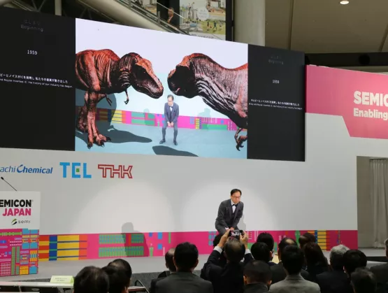
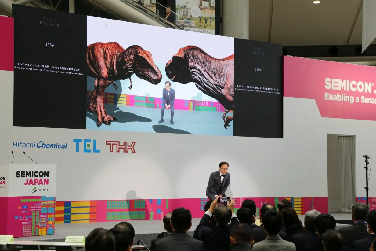
Augmented reality (AR) tyrannosauruses towered on-screen as I interacted with the creatures in a mix of prehistoric and cutting edge. Or, rather, my AR double was doing the playacting. Minutes later, virtual doppelgangers of a small lineup of chip industry executives cut the ceremonial ribbon. Seemingly sweeping away the winter chill, the opening of SEMICON Japan 2019 dazzled with smart technology and the promise of lives, cities and workplaces transformed, with uber-intelligent applications in full display at Tokyo Big Sight. But what resources does the industry need to harness to drive the next era of innovation? The semiconductor industry’s unwavering passion and young talent are key, said Hiroshi Imano, Chairperson of the SEMICON Japan Initiatives Committee, in his opening keynote. And hardly any region of the world is in a better position to help realize that future than Japan, Imano said. The region supplies one third of the equipment and more than half of all materials to the global semiconductor manufacturing industry.Talent was also top of mind for SEMICON Japan 2019 keynote speaker Makiko Eda, Japan's Chief Representative Officer at the World Economic Forum (WEF). Serving as a platform for public-private partnerships, the organization's mandate is to tackle global issues such as climate change and geopolitical strife in making world more resilient to risk and, by extension, more sustainable.Spanning ecology, economy, technology, society, geopolitics and industry, that mission includes reskilling and upskilling a billion people over the next decade, a high priority for WEF, which hosts a conference every January in Davos, Switzerland. The theme of this month's conference – Stakeholders for a Cohesive and Sustainable World – reflects the vital importance of building the international partnerships and global consensus necessary to achieving WEF's goals.One key to that sustainability will be technology and Arm, a global chip design company, will play a key role, with the company’s chips touching over 70 percent of the world’s population, Arm president Yuzuru Utsumi said in his keynote. Today, Arm is driving toward an ambitious goal: Ship 100 billion chips from 2017 to 2021 – the same number produced over the previous quarter century – by powering advances in mobile computing, server and networking infrastructures, and automotive applications.Arm’s innovation ecosystem of more than 1,000 partners will deliver these chips as they continue to work together to develop differentiated technology. Arm plans to increase investments not only in its primary processor business to accelerate market share gains but in the company’s new IoT business to create new revenue streams. The goal: Deliver long-term sustainable growth, Utsumi said. SEMICON Japan 2019 showcases SMART manufacturing and transportation Billed as a showcase of smart technologies, SEMICON Japan 2019 delivered with an array of eye-grabbing exhibitions in the popular SMART Applications Zone. In the SMART Transportation area, the automatic operation pavilion featured a car equipped with open-source software for autonomous driving. The exhibitor, Tier IV, aims to help lead the early commercialization of self-driving vehicles through the adoption of its software, Autoware, which makes it easier to develop self-driving vehicle prototypes using low-power platforms.Sony Semiconductor Solutions demonstrated a vision sensing processor designed to guide autonomous drones. Using two cameras, the processor measured the changing distance between visitors moving about the exhibit and stationary objects in real time, indicating proximity in hues of red (nearby) and blue (at a distance). Many visitors were wowed, describing the multichromatic display as futuristic.Others rode a simple wooden swing hanging by two ropes, but from dizzying heights thanks to Solidray’s Duo-Sight, a virtual reality (VR) system that projects 3D images stretching from wall to floor for immersive experiences. One visitor thrilled at how riding the swing, suspended only a few feet from the floor, felt like soaring on a flying trapeze. Target applications for the technology include virtual rides at amusement parks and presenting interior design options to homeowners.In the SMART Manufacturing area, one highlight was the demonstration by the National Institute of Advanced Industrial Science and Technology (AIST) of a remote-controlled Minimal Fab System designed for low-volume, high-mix chip production with little staffing. Designed to increase production efficiency, the system allows a circuit designer to manufacture a semiconductor by singlehandedly operating equipment up and down the production line. Controlling nearly 50 pieces of equipment, the Minimal Fab System on display manufactured chips that were verified for functional operation and exhibited afterwards.On the SMART Applications stage, exhibitors DENSO and Toyota Motor Corporation announced a new joint venture to conduct research and advanced development of the next-generation in-vehicle semiconductors critical to electric and autonomous vehicle innovation. The venture, operating as MIRISE Technologies, will combine Toyota’s mobility expertise with DENSO’s in-vehicle component prowess. The goal is to build a rapid, competitive development system by 2030, said Yoshifumi Kato, executive director of the DENSO Research and Development Center, and president and representative director of the venture. On track to begin work this year, MIRISE will span three fields of technology development: power electronics, sensing and SoC (System-on-a-Chip). The name MIRISE combines word the Japanese word "mirai" (future) with "rise."Business Continuity PlanningNatural disasters and other emergencies are an ongoing threat to uninterrupted business operations across the semiconductor manufacturing supply chain and particularly in earthquake-prone Japan. To better prepare for business disruptions and restore normal operations as soon as possible after disaster strikes, more companies are teaming on Business Continuity Planning (BCP).THK's Seismic Isolation Experience Car demonstrated one technology designed to help – a seismic isolation device. The car shakes like an earthquake to give people inside a taste of how a building heaves and sways during a quake with and without the device deployed. Visitors were struck by how much the isolator dampens tremors to prevent or minimize damage. In the BCP seminar, representatives from Sony Semiconductor Manufacturing, THK, DISCO and Team Engineering Consulting shared lessons learned from actual disasters and discussed the critical importance of daily disaster drills. Yukihide Keigo, Executive Engineer in charge of Products and Development at Sony Semiconductor Manufacturing, recounted how the company’s Kumamoto Prefecture plant struggled for 96 days to restore full operations after the facility sustained heavy damage in the 2016 earthquake. Keigo said the plant lacked the structural reinforcements necessary to withstand the impact and fell prey to poor planning and accountability. The Kumamoto plant has since implemented measures – structural and procedural improvements – that more accurately account for seismic risks to ensure full recovery within 56 days. The plant’s new procedures include emergency drills for staff including night-shift workers.Innovation abounds at six SuperTHEATER forumsSEMICON Japan 2019 was held in the West and South Halls of Tokyo Big Sight as organizers of the Tokyo Olympics occupied the East Hall, the exhibition's usual home at the venue, to prepare for the 2020 games. For the first time, the main stage, SuperTHEATER, was set up in the cavernous arena near the main entrance. The SuperTHEATER featured six forums over three days. Semiconductor Executive Forum – View by Top Two in the Era of Digitalization with thought leaders from IHS Markit and Sony Semiconductor Solutions SMART Connectivity Forum – Infinite World Brought by 5G Innovation with experts from Softbank and Nokia Solutions Networks SMART Transportation Forum I – Front-line of Automated Driving featuring speakers from Intel and DENSO SMART Transportation Forum II – Revolution of Sky Transportation, supported by the U.S. Commercial Service in Japan, with presenters from Ministry of Economy, Trade and Industry (METI), Subaru and Bell Helicopter Manufacturing Innovation Summit – Issues and Innovation: What will Drive Growth to 2030 featuring thought leaders from VLSI Research, Applied Materials, KLA, Nikon and Tokyo Electron Mirai Vision Forum – Future Relation of Technology and Body 2.0 with speakers from Leave a Nest, Ory Lab and Autonomous Control Systems Laboratory The Mirai Vision Forum highlighted advanced technologies that could lead to societal improvements. One presenter, Kentaro Yoshifuji, CEO at Ory Lab, recalled how, as a child, he once stayed home from school while recovering from an illness. His imagination in full flight, the youngster imagined having a clone that could attend school and be with his classmates. The experience eventually inspired him to develop OriHime, a robot that gives socially isolated people a way to communicate with friends or colleagues remotely. Originally developed for physically impaired people, OriHime today is used to help the able-bodied. The robot is situated with the companion and the user operates OriHime remotely. A camera and monitor in OriHime’s face provide the visual and audio connection and the user controls the device with a smartphone or tablet or, for those who are paralyzed, through eye movement. One potential application: With OriHime stationed at a business office, working mothers could use OriHime to telecommute to better balance their careers with their parenting responsibilities at home. The robot would be a mother’s go-between, enabling her to communicate directly with colleagues.The next generation of innovators also took the stage as five teams presented innovative business ideas in friendly competition. The top prize in The TECH CAMP Hackathon went to the group that hatched an ingenious plan to develop a jacket that trains users to move their bodies in preprogrammed ways. For example, legendary Japanese professional baseball player Shigeo Nagashima could wear the gear while batting to program the device, then give the jacket to someone who’s never swung a baseball bat. The jacket would help the user replicate Nagashima’s swing. Now comes the real work of any innovator – executing on the vision.And then came two soccer-playing artificial intelligence (AI) robots that squared off and ... Scored! The demonstration by the Toyota National College of Technology started as a research project by Toyota National College students in 2002. The young innovators designed and developed all the robotic hardware and software from scratch. Looking ahead to SEMICON Japan 2020!SEMICON Japan 2019 not only gathered leading Japanese semiconductor materials and manufacturing equipment providers to demonstrate their latest innovations. The premiere regional event also provided insights on key trends critical to the entire electronics manufacturing supply chain. This year’s event drew more than 51,000 visitors and 695 exhibitors from 15 regions filling more than 1,700 booths.SEMICON Japan 2020 returns to East Hall at Tokyo Big Sight in December 2020. I look forward to seeing you there!Jim Hamajima is president of SEMI Japan.
Read More
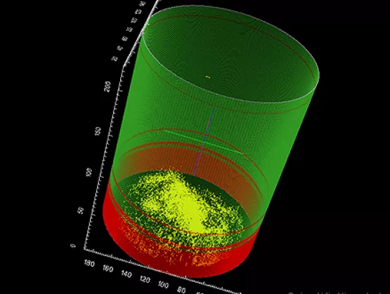
Sapphire is a precious gemstone, consisting of aluminum oxide (α-Al2O3) with occasional traces of other elements such as iron, titanium, chromium, vanadium or magnesium. While sapphire stones found in nature mostly go to jewelry applications, the lab-grown sapphire – produced in a scale of up to several hundred tons per year – is widely used by the electronic industry. Now one can hardly find a branch of technology where this crystal is not used.Sapphires are mainly applied in infrared optical components, high-durability windows, wristwatch crystals, and the very thin electronic wafers used as the insulating substrates of solid-state electronics. High thermal conductivity, low reactivity, and appropriate unit cell size make sapphire an ideal material for a wide range of such electronic substrates for manufacturing of components such as LEDs and CMOS chips.SEMI spoke with Ivan Orlov, CEO of Scientific Visual, after his presentation at SEMI Strategic Materials Conference at SEMICON Europa, 12-15 November, 2019 in Munich, Germany, to learn more about the future of sapphire.SEMI: Why is sapphire an ideal material for a wide range of electronic substrates? Orlov: Sapphire undoubted advantages are its chemical inertness and ability to withstand high temperature, radiation and mechanical loads. In addition, it exhibits low dielectric loss and very good electrical insulation that makes sapphire a good candidate for substrates for LEDs and laser diodes or wafers for epitaxial growth. However, the most important advantage is that sapphire crystal lattice does very well matching semiconductor materials deposited to its surface, in particular nitrides of group III elements. To plainly benefit from these features, the grown sapphire must have as few macro- and micro-defects as possible, as substrate defects are inherited by semiconductors layers grown on the substrate surface. Hence the importance to detect defects in the raw sapphire material. This is the area where our team at Scientific Visual contributes. SEMI: Flaws are usually identified only after costly wafering and polishing steps, because rough surface of raw crystals prevents detection of the defects. What can be done to prevent defects?Orlov: Today, major players are investing in growing larger crystals without mastering in depth the growth process. Let’s face it, the semiconductor substrate industry, which is primarily based in Asia, is using empirical research methods. The raw sapphire boules are still inspected manually, and this qualitative assessment is exploited in two folds. The first step is to further process the boule. Furnace operators then adjust the growing parameters depending on the results of the manual inspection.Due to the lack of visibility into internal crystal defects, the crystal growth and its downstream processing remain an art rather than a science. The primary reasons are the difficulty to measure, locate and quantify precisely the defects in the full crystal volume. Scientific Visual equipment enables defects in raw boules to be fully quantified and categorized. With such objective measurements and knowing the full set of growth parameters, the Process Engineering (PE) team can, with the assistance of deep learning algorithms, considerably improve the growing process. Our quality control tools give Process Engineering team the “eyes” to see complete defect distribution in raw crystals, enabling it to make minor modifications in the growth process to improve yields, reduce costs and shorten the time to market for products.SEMI: What lead to those advancements and what problems did your team set out to solve? Orlov: Breakthroughs in immersion tomography, machine vision and parallel computing drove advancements in automated quality control technology. Previously crystal inspection accuracy was limited by the acuity of the operator’s eye and subjective bias. Light distortion and the diffusion of crystals made it impossible to accurately identify internal defects.Scientific Visual equipment give operators an undistorted 3D view of all defects in a crystal boule or ingot. However, only deep learning technology can correlate a hundred thousand growth data points to identify a final defect pattern.Defect pattern in non-processed item cored from EFG sapphire plate. Well visible is a typical wavy pattern of surface layers and sandwich structure in the volume. Color code marks sapphire defect density: from deep blue (non-defective material) to deep red (highest defectiveness.) SEMI: What challenges are addressed by your approach? Orlov: Increasing the yield of semiconductor substrates like Sapphire, Gallium Nitride and Silicon Carbide is paramount to reducing the price of wafers while increasing their quality. The upstream growth and downstream wafering processes are not deterministic. So far, most of the producers can only determine the quality during the late stages of the process. This condition creates huge constraints for teams in charge of production and processing. Automated Quality Control (QC) at the early stage of the production chain relieves all the unknowns, ultimately reduce the cost of material.SEMI: And what are the main opportunities?Orlov: There are massive opportunities to increase the yield and to ease the full processing chain from growth to the wafering process. Objective Quality Control (OQC) paves the way to industry-wide standards that categorize crystal quality at each step of growth to enable full certification of the defectiveness of the material and facilitate its trade and exchange.SEMI: What’s one of your predictions for the future of new materials?Orlov: The explosion of e-mobility and electric vehicles and the development of other green technologies will drive rising demand for low-defect sapphire, silicon carbide and gallium nitride substrates thanks to the streamlining of the full processing chain. Manual quality control will soon give way to full automation as quality control in sapphire and other raw crystals production is the only missing link in a fully automated semiconductor production chain. I believe that in five years, automated raw crystal inspection will become standard in the industry. Our mission is to empower every crystal grower to achieve this important milestone.Dr. Ivan Orlov obtained a Ph.D. in Crystallography from the Federal University of Technology in Switzerland EPFL and an MSc in Solid-State Physics in Moscow, Russia. Ivan co-founded Scientific Visual in 2010 to answer the challenge of the synthetic crystals industry struggling with high defect yield. Prior to this he worked in a company specialized in diamond optics. He has more than 10 years of experience in R D with focus on optical materials, industrial crystals and non-destructive quality control technologies. Dr. Orlov was a SEMI Task Force member for sapphire standard development in China and collaborates with ISO committee in Switzerland to establish industry-wide sapphire quality standards.Serena Brischetto is senior marketing and communications manager at SEMI Europe.
Read More
The microelectronics industry is entering the era of Cloud Engineering Simulation to slash the costs and risks of new technology development and speed time-to-market in spaces like semiconductors, MEMS sensors, RF front ends, biomedical and driverless cars. In the run-up to SEMICON Europa, 12-15 November, 2019, in Munich, Germany, SEMI spoke with Ian Campbell, CEO of OnScale, about the new paradigm of Cloud Engineering Simulation. Campbell shared his views ahead of the SMART Design Forum, 14 November, 2019, 14:30 to 17:00, in Hall B1, TechARENA 1 at SEMICON Europa. Registration is open. Join the forum to meet experts from OnScale and other key industry influencers. Attendance is free of charge for all SEMICON Europa visitors.SEMI: How did your adventure with OnScale start?Campbell: I’m an engineer. When I was still in high school, I took a night class at Nashville Tech to learn AutoCAD R14, and I’ve been designing and engineering things ever since. I was introduced to Desktop Simulation in my bachelors of mechanical engineering program and used many types of simulation tools for massive design studies at the Aerospace Systems Design Lab at Georgia Tech. I’m a simulation junkie.I started my first Silicon Valley high-tech company, NextInput, in 2012 with Dr. Ryan Diestelhorst (now VP of Strategy at OnScale), to commercialize new ForceTouch and 3D Touch technologies based on our patented MEMS force sensors. At NextInput, we bought hundreds of thousands of dollars of engineering software, but were always frustrated by slow, inaccurate engineering simulation results. We dreamed about running massive simulations on Cloud Supercomputers and creating true Digital Prototypes that could replace costly, time-consuming, and risky physical prototypes.When I got the chance to join the team that became OnScale in 2017, I jumped at the opportunity. At OnScale, we took engineering simulation solvers that had been developed for the U.S. military to run on U.S. Department of Defense and DARPA supercomputers and built a cloud supercomputer platform on Amazon Web Services to run the solvers. The net-net is the world’s first on-demand, infinitely scalable Cloud Engineering Simulation platform. Now, we routinely run massive multi-billion degree of freedom simulations for Fortune 100 companies, including many from the semiconductor and MEMS industries. Since our business model is to charge per core-hour for simulations, the incredible capability we built is cost-effective and available to small startups as well. SEMI: How is the semiconductor design ecosystem evolving? How is Cloud Engineering Simulation applied to semiconductor and design industries?Campbell: The entire industry is experiencing a massive acceleration in product launch cycles and increased competition. New markets like IoT and 5G are reducing semi/MEMS product cycles from years to months. That, in turn, puts enormous pressure on semiconductor and MEMS designers. Missing a key product introduction like a flagship smartphone launch can literally make or break a company.A reliance on traditional engineering methods – schematic capture and layout of a chip, taping out (physically prototyping the chip), performing engineering validation on an e-bench, qualifying the chip (or not qualifying it and going back to the drawing board), and finally launching mass production – is no longer sustainable from a competitive perspective.Instead, market-leading firms are turning to Cloud Engineering Simulation and Digital Prototypes to explore massive design spaces, find optimum designs that beat the competition in every KPI (size, power, performance), and digitally qualify designs before ever cutting silicon, ensuring that designs are robust over their intended operating environments and performance envelopes. Large thermal analysis of a chip on a circuit board executed quickly on the OnScale Cloud Simulation Platform SEMI: Can you give us an example? Campbell: A great example is thermal analysis. Thermal effects have always had huge impacts on MEMS device performance and, more recently, they are beginning to impact performance of next-gen semiconductors, especially GaN power electronics for electric vehicles (EVs).Conducting a full system-level thermal analysis of something like an EV power management system – a power IC in a package, on a board, in an enclosure, under various loading conditions – has been a challenge from a simulation complexity perspective (degrees of freedom) and from a parametric sweep perspective (running hundreds or thousands of simulations to optimize chip placement, routing, etc.). To run these sets of simulations using legacy desktop simulation would take weeks, perhaps even a month or more. To run these massive simulations in parallel on cloud supercomputers using OnScale takes days or even hours.Our customers routinely run very large simulation studies on OnScale Cloud for thermal simulations, RF filter simulations, MEMS simulations, packaging simulations (what we call Digital Qualification), and many more use cases.SEMI: What’s one of your strategic objectives for 2020? Campbell: For 2020, we’re doubling down on MEMS and semi simulation capabilities. We will be launching additional solver capabilities like EM that will be critical in our strategic markets like 5G. We will also be launching a Cloud API so that engineers can integrate OnScale directly into their existing engineering workflows (e.g. MATLAB or EDA/CAD tools) with just a few Python commands.SEMI: Can you share one prediction for the future of semiconductor design solutions? share?Campbell: I think we will continue to see MEMS and semi designers push the envelope and bring smaller, more performant, more cost-effective solutions to market. I’d like to see more highly cost-effective flexible semi/MEMS designs come to market to enable next-gen IoT and IIoT applications. I’d also like to see more biomedical applications – biomems, microfluidics, and labs on a chip for all sorts of life-enhancing applications.SEMI: What are your expectations regarding the SMART Design Forum at SEMICON Europa 2019 in Munich? Campbell: I’m looking forward to getting back to my roots in MEMS/semi design and chatting with other designers about the future of engineering and the future of semi! Ian Campbell is a twice venture-backed Silicon Valley CEO and expert in MEMS sensors, semiconductor technology, and engineering software. Most recently, Ian co-founded OnScale, a Cloud Engineering Simulation startup backed by Intel Capital and Google’s Gradient Ventures. OnScale is revolutionizing engineering by combining world-class multiphysics solvers with Cloud supercomputers, machine learning, and artificial intelligence. Prior to co-founding OnScale, Campbell served as founder and CEO of NextInput, where he led the startup through multiple rounds of funding – totaling $12 million and an additional $4 million in research contracts with government and industry partners – and built a world-class team of engineers and scientists who developed 3D Touch and ForceTouch technologies for smartphones, wearables, industrial, and automotive interface applications. He also secured the first major smartphone OEM design wins in Asia. Campbell earned his B.S. in mechanical engineering from Middle Tennessee State University, and his MSAE in aerospace engineering and MBA from Georgia Institute of Technology.Serena Brischetto is senior manager, marketing and communications, at SEMI Europe.
Read More
Automobiles have become an even more important segment for MEMS and sensors as carmakers integrate more chips for propulsion, navigation, and control into their designs. However, these advanced functions and their crisp rate of adoption have fragmented the sourcing of automotive chips. IHS Markit’s Jérémie Bouchaud provided a closer look at and outlook for this key market at the MEMS and Sensors Executive Congress in late October in Napa. Following are key takeaways from his presentation.Autonomous and Electric/Hybrid Vehicles to Drive MEMS Market GrowthThe automotive market, approaching 100 million vehicles produced annually, is approaching $6 billion, dominated by MEMS and silicon magnetic sensors for chassis and safety, and powertrain applications. Going forward, the market growth will be in autonomous vehicles and electric/hybrid vehicles. Because the penetration of electric and hybrid vehicles is much higher than that of autonomous vehicles, it has a larger available market, particularly for sensors. Each of these markets has its own dynamics.For example, the electric and hybrid market has historically relied on a significant number of traditional, or non-semiconductor sensors, but new sensor technologies are vying to address multiple sensing needs. The most important limitation on demand of autonomous vehicles is the overall market penetration: IHS Markit expects autonomous vehicle production to reach 10 million at most by 2030.Production of Electric and Hybrid Automobiles Now Growing at Fast ClipProduction of electric and hybrid vehicles is in a rapid growth phase, and IHS Markit expects penetration of such vehicles to reach 50% of the automotive market by 2030, up from 3% in 2016. The core functions of charging and power inversion require, among other capabilities, current, temperature and position sensing. Historically, many of these functions have been handled by non-semiconductor devices, for example negative temperature coefficient (NTC) thermistors for temperature sensing, devices that appear to be strongly positioned. In other areas, semiconductor sensors are competing with traditional devices.For example, silicon magnetoresistive devices are going head-to-head with inductive devices for position and Hall effect sensing. Sensing requirements are also likely to evolve over time, particularly as battery systems become more reliable and robust. While some automakers are looking to sensors to monitor pressure or gas leaks from batteries, battery makers are more focused on maturing the systems and reducing the need for monitoring.Autonomous Vehicles Drive New Source of Demand for MEMS and SensorsThe movement towards automated driving has created a new source of demand for MEMS and sensors, with advanced driver assistance systems driving faster growth than the historical powertrain applications. Currently available vehicles are at Level 2 (partial automation), with multiple cameras and radars. Level 3 vehicles (conditional automation) are likely to enter the market next year, adding driver monitoring cameras, LIDAR systems and, potentially, microbolometers or other night-vision systems. Level 4 and 5 (high and full automation, respectively) will add vehicle-to-vehicle communications and other systems, but are not likely to be widely available for several years.The autonomous vehicle market, while smaller overall compared to electric/hybrid vehicles, provides a more attractive opportunity for MEMS devices, particularly in LIDAR systems. LIDAR and other sensing/surveying systems are at the heart of autonomous vehicles, and MEMS devices are in demand for the critical beam-steering function. However, demand for image and other sensors will accelerate as the higher levels of autonomy are rolled out.Automotive Drives Extremely Diverse Set of Applications for MEMS and Sensor MakersThe automotive market presents an extremely diverse set of applications for MEMS and sensor makers. Some companies have developed broad product portfolios and compete in multiple applications. For example, TDK offers NTC thermistors as well as MEMS and silicon-based sensors. Semiconductor companies such as Infineon are competing in MEMS and with silicon-based sensors such as magnetoresitive and Hall effect.The growth in demand for image and radar sensors used in ADAS, as well as magnetoresistive and Hall sensors in EVs, means that the center of gravity in automotive markets is likely to shift from MEMS over the next several years – a fundamental change, Bouchaud cautioned, that will put automotive sensor suppliers focusing solely on MEMS at risk.Paul Semenza is a consultant in SEMI Industry Research and Statistics.
Read More
Powerful winds of change are re-shaping the semiconductor industry as it flexes and re-positions to power a new wave of growth on the back of emerging applications. Today, the industry is thriving, with growth expected to continue through 2019 even as Moore’s Law – the trusty doubling of transistors roughly every two years – begins to pump the brakes. Product mix and production technology are shifting as the dominant smartphone and PC markets, having seen their growth peaks, start to give way to large markets with relatively low semiconductor penetration, such as automotive.What’s more, new potentially ubiquitous technologies and platforms such as AI, blockchain and smart manufacturing are redefining market dynamics and the semiconductor ecosystem that underlies them.Troublingly, the most significant threats to the continued growth of the semiconductor industry are not of its own making. Macroeconomic trends and trade policy disputes loom.These were some of the key takeaways from the SEMI Market Symposium kicking off SEMICON West in San Francisco this week. Following is a deeper look.Semiconductor MarketThe consensus view, reflected in forecasts presented by Clark Tseng of SEMI and Bob Johnson of Gartner, is that the semiconductor industry could top $500 billion in 2019 after reaching $400 billion in 2017. According to Gartner, smartphones and PCs will continue to account for large parts of the market, but will be displaced as major drivers of market growth by the emergence of industrial, automotive and, to a lesser extent, storage, from 2017 to 2022. Johnson noted that while communications and data processing applications drive logic device demand, average sales prices (ASPs) are a bigger contributor to revenue growth than unit growth.Leading-edge processors are a big part of the ASP picture, with equipment costs increasing ~20 percent per node. One challenge is that as Moore’s Law loses steam, leading logic producers are increasingly going their own way with new production technology. The volatile DRAM market – now in a “super cycle,” according to Tseng, and expected to peak in 2019 – has been stoking memory market growth.Initially, supply shortages fueled memory price increases as three of the four leading memory makers invested in flash rather than DRAM capacity. However, memory prices have been more recently been lifted by technology complexity, particularly as DRAM has moved to 3D architectures. The good news is that pricing, at long last, appears to be driven by value.Automotive MarketWith automotive accounting for less than 10 percent of semiconductor demand, there is room for growth. Rudy Burger of Woodside Partners noted that while the end market for automobiles is growing slowly, at 3 percent CAGR, the market size is nearing 100 million units. In market segments such as electric vehicles, the semiconductor content exceeds $1,000 but can be much higher.For example, the BMW i3 sports over $4,000 in semiconductor content. Burger said connectivity, autonomous driving and shared mobility services are also key opportunities for semiconductors to deepen their penetration in automobiles. For instance, the auto market for cameras, is expected to grow from $2 billion in 2017 to $6 billion in 2022.On average, high-end vehicles feature over $1,000 in semiconductor content, whereas low-end vehicles hover in the $400 range, said Anand Srinivasan of Bloomberg. Because the automotive market is segmented by function or subsystem, with different suppliers focusing on different areas, there is little supply concentration. Srinivasan also pointed out that because of significant differences in their objectives, automotive safety and automation systems should be developed separately.BlockchainThe chief benefit of blockchain is the trust it begets among all parties to a digital transaction through four fundamental features, said David Treat of Accenture: The tracking of provenance (knowing who has touched data, and what has happened to it) Tamper evidence (knowing if someone has tried to change the data) Control (which data elements to share with which parties) Security at the data element level While most of the hype over blockchain focuses on tokenized assets and ledgers (bitcoin and other cryptocurrencies), the fundamental application in the semiconductor industry is sharing trusted access to reference data at the data element level. This ability to provide shared trust can reduce costs throughout the supply chain and across enterprises. For example, future blockchain implementations will offer a full ecosystem view to any supply chain participant. While blockchain has typically been deployed through centralized control or platforms, peer consortia, such as SEMI, could help weave the benefits of blockchain through various ecosystems by enabling equipment and material suppliers, device manufacturers, designers and system integrators to share business and technical information securely and, if desired, anonymously.Global and Macroeconomic TrendsThe biggest threats to the continued growth of the semiconductor industry are exogenous. After a decade of steady recovery since the financial crisis, the global economy appears to be heading for a slowdown. Duncan Meldrum of Hilltop Economics made the case that the global economy is at or just past the peak of the business cycle, and semiconductor equipment is past the peak.A key indicator of a looming recessionary is the movement toward an inverted yield curve, in which long-term interest rates fall below short-term rates – a phenomena that could materialize this year or next.The increasingly heated trade climate, marked by high-stakes confrontations between the U.S. and China, threatens complex supply chain arrangements, though mercurial policy statements could do even more harm than stiffer trade tariffs. Underscoring competing interests between the U.S. and China and the unpredictability of their relations, Robert Maire of Semiconductor Advisors pointed out that, in 2019, 60 percent of all semiconductors are expected to be used in China, deepening the dependency of several U.S. semiconductor companies on China.Paul Semenza, for SEMI Industry Research and Statistics
Read More